Later, evaluation of the spin-orbital coupling (SOC) matrix element and the predictive measurements are used to calculate the radiative rate constant kr, and finally the phosphorescent properties and the better performance of the OLED are discussed, which include charge injection/transport and balance ability, the energy transfer rate, and materials for triplet exciton and guest and guest exciton confinement. On the basis of the optimized structures in the excited state, the emission spectra of the considered molecules are investigated.
Experimental procedure
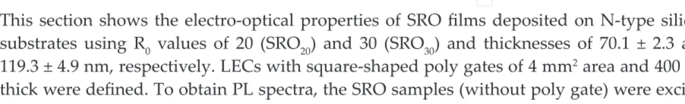
The optical power of the emitted light was measured with a 1400 IL radiometer connected to a UV-VIS GaAsP detector placed in front of the door. Further details on the various characteristics of the studied LECs are discussed in Sections 3.1–3.3.
Results and discussion
SRO monolayers
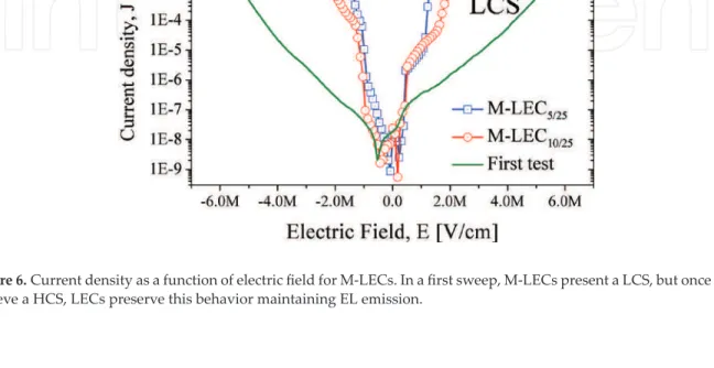
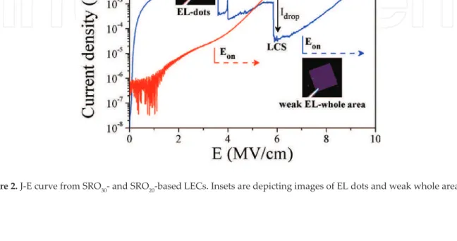
Recent reports of the same electrical switching in SRO films have been observed, which have been linked to the presence of a conductive nanofilament [21–24]. During the HCS regime, current spikes and dips corresponding to the appearance or disappearance of electroluminescent dots (EL dots) on the LEC surface were observed (see the inset of Fig.
SRO monolayers on textured substrates
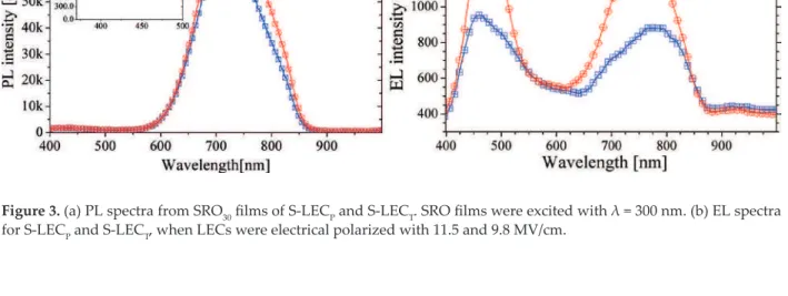
At medium electric fields (region II), the Fowler-Nordheim tunnel mechanism is responsible for the conduction. At the higher electric fields (region III), the trap-assisted tunneling mechanism controls carrier transport.
SRO multilayers
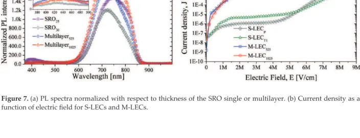
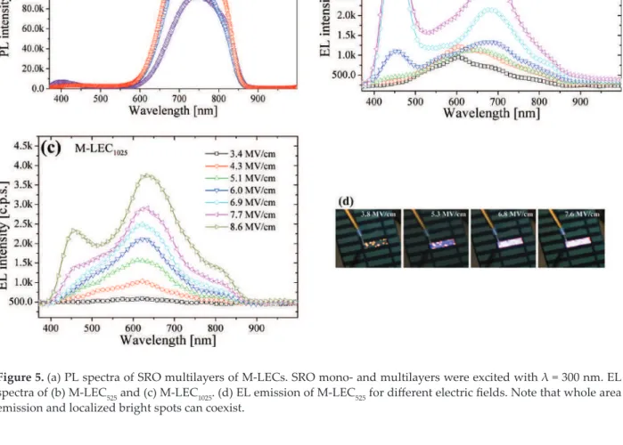
As reported in [37], Si-ncs are observed in multilayer SROs, and their size and density depend on the properties of each layer (excess silicon, thickness, etc.), in agreement with other reports on multilayers. Figure 5(d) shows digital images of the EL emission of M-LEC525 biased with different electric fields, where the emission is dominated by blue color.
Discussion
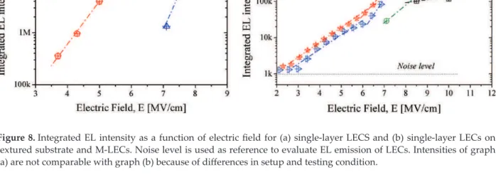
These figures allow the LEC to be compared using two values: the cut-on electric field (Eon) and the operating range. The eon is the electric field required for the EL intensity to exceed the noise level and begin to increase; meanwhile, the operating range is the region of the electric field in which LECs emit light without electrical damage, and must pass from the Eon value to the E value before the dielectric breaks down. Accordingly, devices without Si-ncs in SRO films and emitting in blue wavelengths require a higher electric field (E > 7MV/cm) to turn on.
Integrated EL intensity as a function of electric field for (a) single-layer LECS and (b) single-layer LECs on structured substrate and M-LECs. In addition, the EON value of M-LECs is lower than that of S-LECs, and the EL intensity of M-LECs gradually increases as the electric field becomes stronger. In contrast, S-LECs require a higher electric field to emit light, and their transition from turn-off state to turn-on state is abrupt.
Conclusion(s)
Therefore, M-LECs are better candidates to be integrated into silicon photonic circuits due to the lower Eon and wider operating range. A higher operating range, lower Eon values, an EL intensity that gradually increases, and a larger Popt are the features that position M-LECs as the best option to be integrated into silicon photonic circuits. In [4] it has been demonstrated that S-LECs are enough to guarantee the functionality of silicon photonic circuits; However, the LECs operate close to the noise level.
Furthermore, M-LECs emit at lower electric fields and their intensity gradually increases as the electric field becomes stronger. Therefore, M-LECs perform a better behavior for integration into all-silicon photonic circuits based on a lower Eon and a wider operating range. A higher operating range, lower Eon, gradually increasing EL emission and a larger Popt are the features that make M-LEC the best option for integration in all-silicon photonic circuit.
Acknowledgements
Electro-optical characterization of different LECs showed that M-LECs have twice the operating range of S-LECs. In contrast, S-LECs require a high electric field to emit light, and their transition from the off state to the on state is abrupt.
Conflict of interest
Author details
Intense electroluminescence in the entire region of low-pressure chemical vapor deposition silicon-rich oxide-based light-emitting capacitors. 6] Alarcón-Salazar J, López-Estopier R, Quiroga-González E, Morales-Sánchez A, Pedraza-Chávez J, Zaldívar-Huerta IE, Aceves-Mijares M. Silicon-Rich Oxide Obtained by Low Pressure Chemical Vapor Light Sources to Develop Silicon.
25] Aceves-Mijares M, González-Fernández AA, López-Estopier R, Luna-López A, Berman-Mendoza D, Morales A, Falcony C, Domínguez C, Murphy-Arteaga R. On the origin of light emission in a silicon-rich oxide obtained by low-pressure chemical vapor deposition. Enhancing the emission and conductivity of light-emitting capacitors with silicon-rich oxide multilayer structures.
TOP 1%
Multifunctional Optoelectronic Device Based on Resistive Switching Effects
Introduction
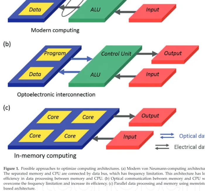
Optoelectronic interconnection is a viable method to overcome the bottleneck by transmitting data between memory and CPU via photons, which have much higher transport speed, higher bandwidth, no Joule heat, and no interference over electrons [1–10]. However, the electronic memristor based architecture still has a bandwidth limitation in high frequency data communicating between different modulators. The combination of photons and memristor-based circuits will integrate the advantages of photons in high-speed data transmission and memristors in parallel in-memory computing and could open a new era for future computing thanks to its high bandwidth and low power consumption.
Moreover, the optoelectronic-based memristive system will extend the application of memristor-based architecture to image or visual information processing. The optoelectronic memristor-based architecture, where both photons and electrons are used for parallel data processing and communication between input-output (I/O) devices and the in-memory processor, can provide such a platform for mobile computing. In the in-memory processing unit, a core has the ability to process and store data in situ.
Optoelectronic resistive switching materials and devices
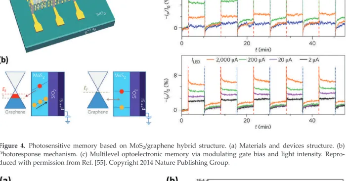
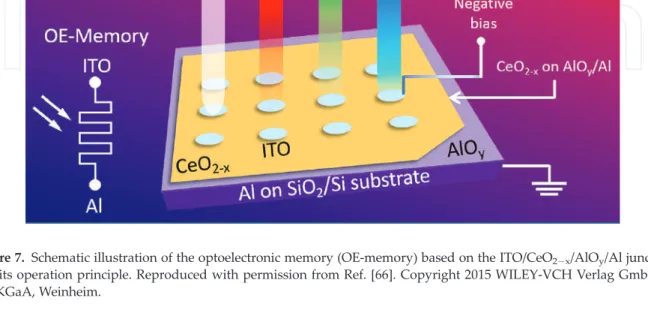
In this work, light pulses with different wavelengths and intensities were used to study the photoresponsive behavior of the memory, as well as to achieve a multi-level and multi-functional optoelectronic resistive switching memory. This work demonstrated that the metal/Al2O3/SiO2/Si structure device can function as a multifunctional optoelectronic device, including information storage and light sensing, while offering the possibility of exploiting an additional optical stage in resistive switching memory devices. Besides Si, ZnO is another type of typical photosensitive semiconductor and has been extensively investigated for UV detectors as well as resistive switching memories [35, 49].
In 2012, Ye reported a multi-level optoelectronic switching memory shown in Figure 5 using a donor-bridge-acceptor (DBA) conjugated molecule, which responds to both optical and electrical stimuli [56]. Under dark conditions, Al/metal conjugated DBA/ITO structured devices showed a bi-stable resistive switching behavior. In a brief summary, trapping and removal of photo-induced charges play the main role in the resistive optoelectronic switching effect.
Multifunctional optoelectronic logic and memory
The non-volatile resistance states can be reversibly switched between high resistance state (HRS) and low resistance state (LRS) by visible light pulse and voltage, thus acting as an optical write and electrical erase memory. Based on this linear relationship between photocurrent and the number of light pulses, counters and adders of the number of light pulses can be realized, and the details are shown in Figure 10b. Only when both a light pulse and a voltage pulse are present is the output value greater than 150 nA, which is logic "1," otherwise the output current is lower than 150 nA, which is logic "0." Also, the "AND" port can be reconfigured to "OR".
In addition to the reconfigurable "AND" and "OR" logic functions, "NOT" operation and a complex logic operation were achieved by introducing another electrical erase pulse, as well as optical adder. The work "NIMTE" encoded in light pulses according to ASCII code can be demodulated and stored in non-volatile resistive states. Two images with "X" and "Y" shapes of visible light pulses are used as input in a 5 by 5 memlogic array and current map as output (Figure 14a).
Optoelectronic neuromorphic devices
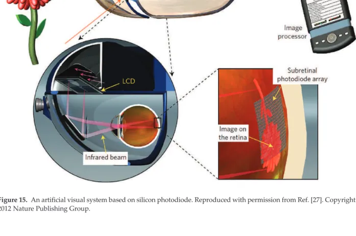
In general, two parts for observing and processing visual information make up the visual system. In recent years, inspired by human visual system, various kinds of artificial visual systems have been proposed to simulate eyes for visual information processing, retinopathy therapy and reproduction of visual system. The design of this artificial visual system provides a new approach to integrate different devices to achieve more multifunctional bio-inspired systems.
Thanks to the reported works, these new promising optoelectronic synaptic devices have been proposed and achieved and will be the first step for optoelectronic neural networks. Optoelectronic artificial neural networks offer the additional advantage of optical communication in memristor-based neuromorphic architectures. Based on previous research, the future plan should focus on improving their performance, using artificial optoelectronic neural networks and optogenetic neural networks.
Other approaches for multifunctional resistive switching
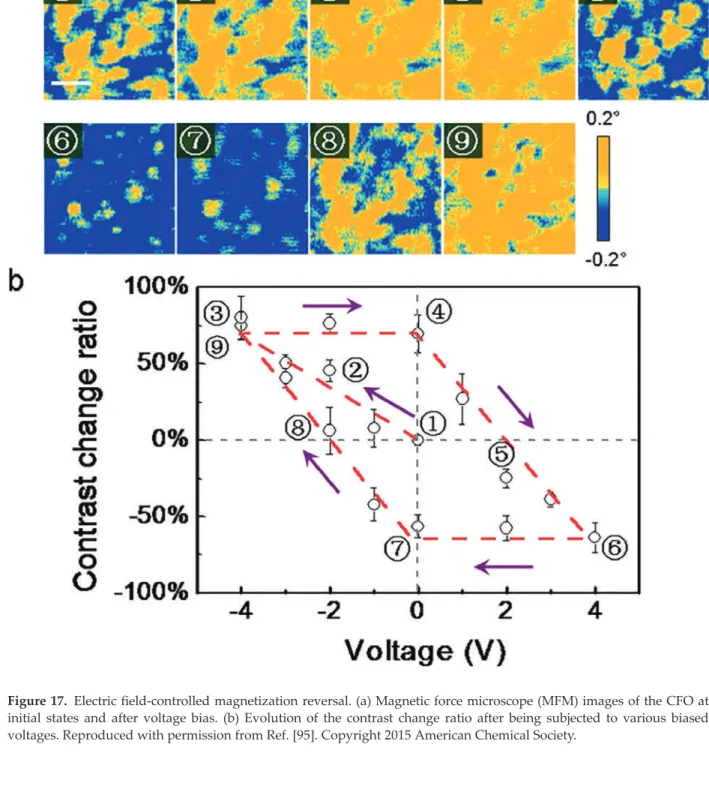
Recently in our group, a nanochannel device was designed in V2O5-based selector via electric field-induced ion migration [94]. This work proved that electric field-induced nanoscale ion migration is an effective approach to optimize device performance or design new conceptual devices. Electric field controlled magnetization reversal. a) Magnetic force microscope (MFM) images of the CFO at initial states and after voltage biasing.
Using the electric field-induced ion migration method, our group also achieved nanoscale magnetization reversal in cobalt ferrite (CFO) thin film.
Challenges and possible approaches
Such nanoscale magnetization modulation by nanoionics may provide a novel approach to manipulate the magnetization of magnetic materials for low-power magnetic memory and spintronics.
Conclusions and prospects
Device-level characterization of light flow in photonic integrated circuits using ultrafast photomodulation spectroscopy. 21] Borghetti J, Snider GS, Kuekes PJ, Yang JJ, Stewart DR, Williams RS. Memristive switches enable 'stateful' logical operations through the implication of materials. 23] Xia Q, Robinett W, Cumbie MW, Banerjee N, Cardinali TJ, Yang JJ, Wu W, Li X, Tong WM, Strukov DB, Snider GS, Medeiros-Ribeiro G, Williams RS.
Intrinsic and interfacial effect of electrode metals on resistive switching behavior of zinc oxide films. Voltage-switchable photocurrents in single-walled junctions of carbon nanotubes and silicon for analog and digital optoelectronics. Low-energy oxide-based electronic synaptic device for neuromorphic visual systems with device variation tolerance.