Focusing on the bandgap of the double junction solar cell, it has been shown to be more efficient compared to the single junction solar cell. This demonstrates that a significant amount of efficiency can be achieved with a multi-junction III-V solar cell.
INTRODUCTION
HISTORY
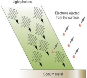
8 The entire PV technology is based on the photoelectronic effect invented by Albert Einstein in 1905. In 1954, the world was introduced to the first photovoltaic module that was just a solar battery. The two most recognized power plants are the Solar Star PV plant which produces 550 megawatts.
WORKING PRINCIPLEOF PHOTOVOLATIC CELL
The modules can therefore be connected in series or parallel, which is very beneficial for the system. 11 But typically in the case of other formation of solar cells, such as crystalline silicon, solar cells are not 100% efficient in diagram.
![Figure 1.3 (a) Layers of photo voltaic cell (b) Energy absorption of photo voltaic cell[1]](https://thumb-ap.123doks.com/thumbv2/filepdfnet/10721778.0/30.918.246.678.598.897/figure-layers-photo-voltaic-energy-absorption-photo-voltaic.webp)
TYPES OF PHOTOVOLATIC TECHNOLOGY
Thin Film PV
The general procedure is to follow the sunlight from east to west during the day. The importance of this type is that it can deliver 30% to 40% more energy, which is more than a fixed array.
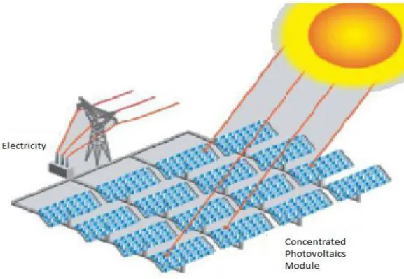
Concentrated PV (CPV)
13 The basis of this technology is the use of inexpensive materials such as mirrors or plastic lenses to track the sun's energy and focus it on solar PV cells. The main reason for using CPV is to reduce the number of solar cell material.
MATERIALS DEVELOPMENT
THE NEXT GENERATION PHOTO VOLTAICS CELL
And this is the maximum current capacity of the solar cell at any illumination level. In addition, the band gaps of adjacent layers should differ as little as possible, since the amount of excess energy from light converted into heat is equal to the difference between the photon energy and the gap of the absorbing material [39]. the semiconductor material determines how the solar cell reacts to light.
RECENT IMPROVEMENTS ON PHOTO VOLTAIC CELL
Improved Efficiency
Their technology was based on an intermediate process that occurs between sunlight and the solar cell, where the photoluminescent material used absorbs radiation from the sun, which converts the heat and light from the sun into an "ideal". As a consequence, a higher conversion efficiency was ensured and the device efficiency was increased from 30% to 50%[6].
Solar Fabrication Using Maximum Voltage from CdTe
Introducing Hot Solar Cell
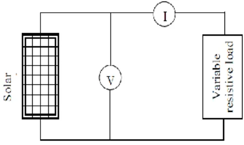
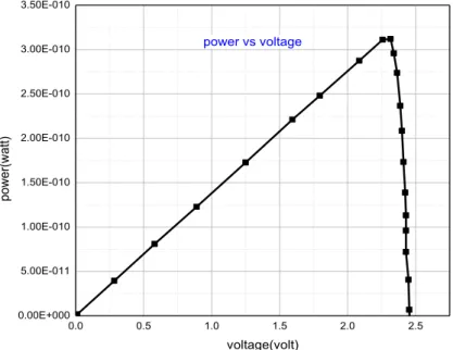
The conversion efficiency of a solar cell is the ratio of the maximum output power generated to the input or accidental power that can be generalized by η. The amount and intensity of solar insolation (solar radiation) controls the amount of output current ( I ), and the operating temperature of the solar cells affects the output voltage ( V ) of the PV array.
Developing Home Systems in Bangladesh
Installation and Plans by BPDB
Bangladesh Power Development Board (BPDB) has also installed solar power plants in various parts of the country. In addition, IDCOL has financed nine biogas-based power plants, with a total capacity of 618 kW, and two rice husk-based power plants with a total capacity of 650 kW in the country.
New Solar Panel in Market 2017
To solve this problem, the innovative manufacturer is making inverters that can be easily attached to the back of the panel. The modules are planned to be manufactured with small inverters already located on the back of the panel.
CONCLUSION
The simple claim is that double-sided panels can capture light as it reflects from the roof or ground surface below the panel. Due to the fact that the majority of roofs in the residential market are black, in order to maximize light reflection, the installers will typically paint a white border around the solar system before installation.
INTRODUCTION
THEORATICAL APPROACH
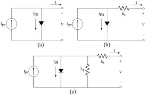
- Equivalent Circuit
- Short Circuit Current
- Open Circuit Voltage
- Maximum Power
- Fill Factor
This is the current that flows through the external circuit when the electrodes of a solar cell are short-circuited. These three important parameters (𝑉𝑜𝑐, 𝐼𝑠𝑐and FF) as described above are the main factors that determine how efficient a solar cell is and are optimized for efficient solar cell design.
![Figure 2.1 Incident light on a typical PN Solar Cell [2]](https://thumb-ap.123doks.com/thumbv2/filepdfnet/10721778.0/43.918.301.765.375.657/figure-2-incident-light-typical-pn-solar-cell.webp)
PRACTICAL APPROACH
- Solar Area Mounting and Tracking
- Improving Solar Efficiency Using Simple Mirrors and
- Improved Perovskite Solar Cell
- High Efficient Ga-As-P Solar Cell
- A Micro-scale Photo Voltaic Cell “Solar Glitter”
Therefore, the improvement of solar cells is very important so that a smaller number of arrays can produce more electricity. Step 3: A rose petal-like film was placed as the top layer of the solar panel to capture even more light.
![Table 2.1 Azimuth Angle by heading [13]](https://thumb-ap.123doks.com/thumbv2/filepdfnet/10721778.0/46.918.256.747.784.1075/table-2-1-azimuth-angle-by-heading-13.webp)
LATEST INNOVATIONS
- Cool Earth Inflatable Solar Balloons
- Moth Eyes Biomimicry for Solar Cell
- Printed Solar Panel “Nanosolar”
- Convertion of Infrared Light to Electricity
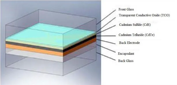
- CdTe Solar Panel
Because of this, such solar panels have a theoretical absorption limit of 63%, which compares to around 40% for ordinary solar cells. The US National Renewable Energy Laboratory (NREL) has created thin-film solar panels that come very close to competing with their more traditional silicon-based cousins.
CONCLUSION
However, the efficiency of CdTe is less susceptible to cell temperature increases, enabling CdTe solar modules to generate relatively more electricity under high ambient (and thus high cell) temperatures. As a result, under real-world conditions, CdTe will generally produce more electricity than a conventional solar module with similar power ratings [15].
INTRODUCTION
OPERATING PRINCIPLE OF SOLAR CELL
44 energy conversion, but in practice almost all photovoltaic energy conversion uses semiconductor materials in the form of a p-n junction.
RESEARCH WORK RELATED TO SOLAR DEVICES
Analytical Method
- Solar cell parameters
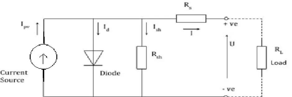
- Effect of Rs and Rsh Parameters
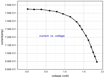
As a result, the voltage-controlled portion of the I-V curve begins to fall far from the origin, causing a significant reduction in the terminal current I and a slight reduction in VOC. As a result, the current-controlled portion of the I-V curve begins to slope toward the origin, causing a significant decrease in the junction voltage V and a slight decrease in Isc, the short-circuit current.
Effect of Temperature
D = given minority carrier diffusivity for silicon as a function of doping in the silicon material. The equation above shows that the temperature sensitivity of a solar cell depends on the open circuit voltage of the solar cell, with higher voltage solar cells being less affected by temperature.
SIMULATION ANALYSIS
Why We Need the Simulation
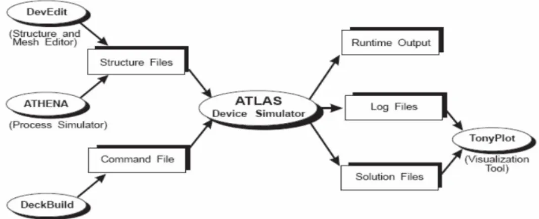
Based on the TCAD device design, the physical parameters that contribute to the resistances between the connections can be extracted and a system-level model developed. From the system cell level model, checks can be made to determine the effect of different cell widths on module performance.
TCAD (Technology Computer Aided Design)
- TCAD Tools
- TCAD simulation process
- TCAD work flow
It takes a spice file as input and produces output describing the requested simulation of the circuit. Manufacturing manufacturing modeling is called Process TCAD, while device operation modeling is called Device TCAD.
Parameters That Can be changed
EXPERIMENTAL ANALYSIS
- For The Measurement of External Characteristics
- Measurement in Different Wavelengths
- For the Measurement of Internal Characteristics
- Measurement of Electro-luminiscence
Here we are observing various changes in the solar cell due to the effects of less and less light and different wavelengths of light on the PV cell and the temperature of the cell. When sunlight falls on the solar cell, the curve begins to move downward. a) (b) (c) Figure 3.15 Change of I-V characteristic curve with increasing incident light.
RESULT FOUND FROM THESE METHODS
CONCLUSION
INTRODUCTION
VIRTUAL WAFER WEB
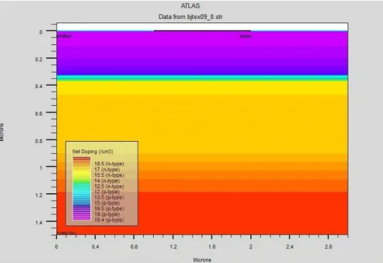
We used double junction solar cell as a reference model for multi junction solar cell. For silicon single junction solar cell, we used three different materials (boron, arsenic, silicon) as the n-layer.
SIMULATION for ELECTRICAL CHARACTERISTICS
Functions of The Simulator
Inputs and Outputs
MODEL EXTRACTOR
DEVICE EDITOR
VISUALIZATION TOOL
SIMULATION PROCEDURE OVERVIEW
Modes of Operation
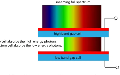
Solar Junction's multi-junction solar cell consists of several individual solar cells grown on top of each other. We noticed that the efficiency is much higher than the single junction solar cell.
Starting with Model Extractor
Syntex
Structure Specification
POSITION -defines the location of the region in terms of (1) actual position and (2) grid nodes. Atlas also provides a standard list of parameters for the properties of the material used in the simulation.
Result Analysis
Here we analyze two specific solar cells: a single-junction solar cell and a multi-junction solar cell. Secondly, in the case of single junction solar cells, the phosphorus doped silicon solar cell is better (both in terms of efficiency and fill factor) than all other single junction cells.
Extract Description
CONCLUSION
Thus, TCAD tools provide researchers with the electrical properties of solar cells under illumination in two- and three-dimensional domains. Two simulation inputs consisting of a text file and a simulation file are made using Deckbuild and Devedit.
INTRODUCTION
SILICON SOLAR CELL
WORKING PRINCIPLE
The electricity was produced by a series of solar cells converting solar energy into a usable amount of direct current (DC).
DUAL JUNCTION SOLAR CELL
PARAMETERS TO BE CONSIDERED
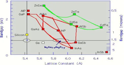
Lattice Match
94 Further InxGa1-xAs at X can be alloyed with InP to obtain a quaternary alloy InxGa1- xAsyP1-y, whose properties lie on the line connecting X and InP and thus all have the same lattice parameter as InP, but different bandgap- layers of InxGa1- xAsyP1-y with composition between X and InP can be grown exponentially on InP substrate by various techniques such as liquid phase epitaxy or molecular beam epitaxy.
Bandgap
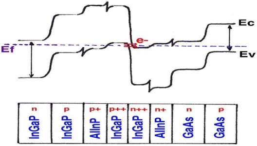
- Structure
- Metal contacts
- Window layer and back surface layer
- Anti reflective (AR) coating
- Tunnel junction
The back surface field, or BSF, consists of a higher doped region on the back surface of the solar cell. To avoid reducing the performance of the MJ solar cells, the tunnel junctions must be transparent to the wavelengths absorbed by the following photovoltaic cell.
CONCLUSION
INTRODUCTION
Throughout our analysis, we have approached versatile techniques that we look right now. So we have always tried to achieve the highest efficiency and fill factor by applying various measures.
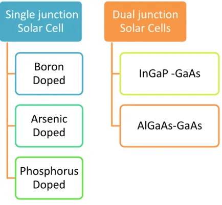
SINGLE JUNCTION SOLAR CELL
Boron doped silicon solar cell
From the I-V curve, P-V curve and the Voc, Isc parameters we obtain further curves to study the filling factor and efficiency of the cells. But we could not find any significant change of fill factor with concentration as the curve appeared random.
Arsenic doped silicon solar cell
Initially, the efficiency increased, but later, with increasing concentration, the efficiency decreased. The curve is random and maintains a sequence of increasing and decreasing fill factor with increasing.
Phosphorus doped silicon solar cell
We obtained the highest efficiency for phosphorus-doped silicon solar cell (18.55%) and the lowest for boron-doping (18.2%). We obtained almost the same fill factor (84.347%) for arsenic-doped solar cell and finally the lowest for boron-doping (83.53%).
DUAL JUNCTION SOLAR CELL
InGaP-GaAs Dual Junction Solar Cell
AlGaAs-GaAs Dual Junction Solar Cell…
There is a small difference in filling factor between InGaP-GaAs and AlGaAs-GaAs solar cells. In our next section we tried to improve the InGaP-GaAs solar cell by changing the concentration or replacing the back material.
InGaP-GaAs DUAL JUNCTION SOLAR CELL
- Concentration Increasing
- Concentration Decreasing
- Changing Back Surface
- Increasing Concentration for New BSF
- Concentration Change for Wider Bandgap for New BSF
- Concentration Change for Wider Bandgap for New BSF
From the above discussion, we can form a table in which we can summarize and show the change in efficiency for increasing concentration of InGaP and GaAs. In this case we get a higher efficiency as we reduce the concentration of the intersections.
CONCLUSION
CONCLUSION
RECOMMENDATION FOR FUTURE WORK
![Fig 3.6 Effect of shunt resistance on the current–voltage characteristics[21]](https://thumb-ap.123doks.com/thumbv2/filepdfnet/10721778.0/70.918.261.700.796.1017/fig-effect-shunt-resistance-current-voltage-characteristics-21.webp)