PLANAR YAGI ANTENNA DESIGN
MOHD SUPIAN BIN SULAIMAN
This report is submitted in partial fulfillment of the requirements for the award of Bachelor of Electronic Engineering (Telecommunication E1ectronics)With
Honours
Faculty of Electronic and Computer Engineering Universiti Teknikal Malaysia Melaka
UNIVERSTI TEKNIKAL MALAYSIA MELAKA
FAKULTI KEJURUTERAAN ELEKTRONIK DAN KEJURUTERAAN KOMPUTER
BORANG PENGESAHAN STATUS LAPORAN
PROJEK SARJANA MUDA I1
Tajuk Projek : -
EGANARYAGI-A_N_TENA_D_ESISN-
- - -Sesi
Pengajian : ... 200412008
Saya ... MOHD SUPIAN BIN SULAIMAN (HURUF BESAR)
mengaku membenarkan Laporan Projek Sarjana Muda ini disimpan di Perpustakaan dengan syarat- syarat kegunaan seperti berikut:
1. Laporan adalah hakmilik Universiti Telcnikal Malaysia Melaka.
2. Perpustakaan dibenarkan membuat salinan untuk tujuan pengajian sahaja.
3. Perpustakaan dibenarkan membuat salinan laporan ini sebagai bahan pertukaran antara institusi pengaj ian tinggi.
4. Sila tandakan ( 4 ) :
(Mengandungi maklumat yang berdarjah keselarnatan atau
SULIT* kepentingan Malaysia seperti yang termaktub di dalam AKTA RAHSIA RASMI 1972)
TERHAD* (Mengandungi maklumat terhad yang telah ditentukan oleh
organisasilbadan di mana penyelidikan dijalankan)
/i-
/
iNGAN PENYELIA) Alamat Tetap: l - 3 @ - D L K ~ . ~ ~ ~ - - -
~ B N P m w B M . - - - Z O m L ABIDIN BIN ABD A n
kcturer
U~IQ, K U A L A - E ~ G ~ ~ A ~ ~
-
Faculty Electronics and Computer Engineering(m
Jkwn.JMfQL- Universiti Telmikal Malaysia Melaka (UTeM)Locked Bag 1200
Ayer Keroh. 75450 Melaka.
"I hereby declare that this report is result of my own work except for quotes as cited
in the references."
...
Signature :"I hereby declare that I have read this report and in my opinion this report is
sufficient in terms of the scope and quality for the award of Bachelor of Electronic
Engineering (Telecommunication Electronics) ,'-- With Honours."
if T
;)If-
Signature
...
r;.....
...
Supervisor's Name :
Date
.
.
,..
...
MOHAMAD ZOINOL ABIDIN BIN ABD AZIZ LectIuf?r
Faculty ElecM)nics and Computer Engieering (FKEKK)
Universiti RlmiM Malaysia Melaka (UTeM)
ACKNOWLEDGEMENT
First, thanks to ALLAH SWT for helping me trough this all the obstacles that
I faced during this project.
I would like to express my appreciation to my supervisor, Mr Mohamad Zoinol Abidin Bin Abdul Aziz that for his guidance and support that help me finished my thesis. For his wisdom, insight and knowledge, the social grace with which he delivers his idea are a constant inspiration. He guided me so that I will continue to be in the correct path during the development of this draft. He provided a motivating and enthusiastic atmosphere during the many discussions we had. It was a great pleasure to do this thesis under his supervision.
ABSTRACT
ABSTRAK
TABLE OF CONTENT
CHAPTER TITLE
PROJECT TITLE
REPORT STATUS RECOGNITION FORM DECLARATION SUPERVISOR DECLARATION DEDICATION ACKNOWLEDGEMENT ABSTRACT ABSTRAK
TABLE OF CONTENTS LIST OF TABLES LIST OF FIGURES
LIST OF ABBREVIATIONS LIST OF APPENDIX
INTRODUCTION
1.1 Introduction
1.2 Problem Statement
1.3 Objective
1.4 Scopes of Project
1.5 Methodology of Project 2
LITERATURE REVIEW 4
2.1 Microstrip Antenna
2.1.1 Introduction
2.1.2 Advantages of Microstrip Antenna 2.1.3 Disadvantages of Microstrip Antenna 2.1.4 Various Microstrip Antenna Configuration
2.2 Planar Antenna
2.3 Yagi-Uda Antenna
2.4 Feeding Technique
2.4.1 Microstrip Transmission Line 2.4.2 Coaxial Feed
2.4.3 Aperture Coupled Feed 2.4.4 Proximity Coupled Feed 2.5 A n t e m Parameter
2.5.1 Resonant Frequency 2.5.2 Gain
2.5.3 Bandwidth 2.5.4 Impendence 2.5.5 Polarization 2.5.6 Efficiency
2.6 WLAN
2.6.1 Advantages of WLAN
I11 PLANAR YAGI ANTENNA DESIGN 20
3.1 Introduction 20
3.2 Design Specification 21
3.3 Antenna Design Procedure 2 1
3.3.1 The Determination of Driven Element 24
Director
3.3.3 The Determination of Director length 3.3.4 The Determination of the Number Director 3.3.5 The Final Design of Antenna
3.4 Fabrication Process
3.5 Measurement Setup
3.5.1 Return Loss Measurement 3.5.2 Radiation Pattern Measurement 3.5.3 Gain Measurement
RESULT AND ANALYSIS 33
4.1 Planar Yagi Antenna with One Director 3 3
4.2 Planar Yagi Antenna with Three Directors 3 6
4.3 Measurement Result 40
4.3.1 Radiation Pattern Planar Yagi Antenna 40
with One Director
4.3.2 Radiation Pattern Planar Yagi Antenna 41
with Three Directors
4.3.3 HPBW and FNBW for Planar Yagi Antenna 42
with One Director
4.3.3.1 For E-plane 42
4.3.3.2 For H-plane 43
4.3.4
HPBWandFNBWforPlanarYagiAntenna
44with Three Directors
4.3.4.1 For E-plane 44
4.3.4.2 For H-plane 45
4.3.5 Return Loss 46
4.3.6 Compared Result between simulation and measure 47
4.4 Analysis of Planar Yagi antenna parameter 49
4.4.1 The Effect Adjusting Driven Dipole Length 49
Director
3.3.3 The Determination of Director length 3.3.4 The Determination of the Number Director 3.3.5 The Final Design of Antenna
3.4 Fabrication Process
3.5 Measurement Setup
3.5.1 Return Loss Measurement 3.5.2 Radiation Pattern Measurement 3.5.3 Gain Measurement
RESULT AND ANALYSIS 3 3
4.1 Planar Yagi Antenna with One Director 3 3
4.2 Planar Yagi Antenna with Three Directors 36
4.3 Measurement Result 40
4.3.1 Radiation Pattern Planar Yagi Antenna 40
with One Director
4.3.2 Radiation Pattern Planar Yagi Antenna 41
with Three Directors
4.3.3 HPB W and FNB W for Planar Yagi Antenna 42
with One Director
4.3.3.1 For E-plane 42
4.3.3.2 For H-plane 43
4.3.4 HPB W and FNB W for Planar Yagi Antenna 44
with Three Directors
4.3.4.1 For E-plane 44
4.3.4.2 For H-plane 45
4.3.5 Return Loss 46
4.3.6 Compared Result between simulation and measure 47
4.4 Analysis of Planar Yagi antenna parameter 49
4.4.1 The Effect Adjusting Driven Dipole Length 49
Reflector
4.4.3 The Effect Adjusting Director Element Length 53
4.4.4 The Effect Adding Director 55
DISCUSSION, CONCLUSION AND FUTUREWORK 57
5.1 Discussion
5.2 Conclusion
5.3 Future work
...
X l l l
LIST OF TABLES
NO.
2.1
3.1
3.2
3.3
TITLE
Comparing the different feed techniques Design specification
The change of RL, f and
B W
due to change driven length The change of RL andB
W due to change of spacing betweenreflector and driven
The change
B
W and RL due to change of director lengthThe change of RL and
B
W
due to change of number of director. The result of simulation and measurementThe result of simulation and measurement of
HPB
W
andFNBW
PAGE
12
2 1
24
LIST OF PIGURES
NO. TITLE
Methodology flow
Microstrip antenna cnfiguration Basic shape of patch antenna The planar radiating element
Yagi antenna structure Microstrip line feed Coaxial feed
Aperture coupled feed Proximity coupled feed
Planar Yagi antenna intial design Dielectric layer setup
Boundaries setup Dimension setup EM layout setup
The layout of EM structures of driven element
The layout of EM structures of spacing between driven and reflector The layout of EM structures of driven element when length of director
is adjusted.
The EM layer of antenna with added director The EM layout of final design antenna The fabricated planar Yagi antenna
Network analyzer
The EM layout of planar Yagi antenna with one director
RL for planar Yagi antenna with one director
VSWR for planar Yagi antenna with one director
Radiation pattern of planar Yagi antenna with one director
Radiation pattern at E-plane for planar Yagi antenna with one director Radiation pattern at H-plane for planar Yagi antenna with one director The EM layout of planar Yagi antenna with three director
RL for planar Yagi antenna with three directors
VSWR for planar Yagi antenna with three directors
Radiation pattern for antenna planar Yagi with three directors
Radiation pattern at E-plane for planaryagi antenna with three directors Radiation pattern at H-plane for planar Yagi antenna with three directors E-co E-cross H-co H-cross E-co E-cross H-co H-cross
E-plane HPB W and FNB W for planar Yagi antenna with one director H-plane HPB W and FNB W for planar Yagi antenna with one director E-plane HPBW and FNBW for planar Yagi antenna with three directors E-plane HPBW and FNBW for planar Yagi antenna with three directors
RL for planar Yagi antenna with one director
RL for planar Yagi antenna with three director
The result of simulation and measurement of RL for planar Yagi antenna with one director
The result of simulation and measurement of RL for planar Yagi antenna with three director
The return loss graph when length of dipole is adjusted 5 0
Spacing between driven and reflector vs. B W 5 1
Spacing between driven and reflector vs. RL 5 2
The simulation RL result when the spacing between driven and reflector is 52 adjusted
Director Length vs. B W 5 3
Director Length vs. RL 54
RL when director length is adjusted 54
The number of director vs. BW 55
The number of director vs. RL 5 5
xvii
LIST OF ABBREVIATIONS
BW
-
CAD
-
dB
-
dBi
-
dBm -
E-plane
-
f
-
FNBW
-
FR4
-
GHz
-
h
-
HPBW
-
H-plane
-
L
-
LAN
-
mm
-
MOM
-
MSA
-
S
-
SUA
-
SWR
-
tan 8
-
uv
-
Bandwidth
Computed Aided Drawing Decibel
Decibel over isotropic
Power ratio in decibel of measured power Electric field plane
Frequency
Full Null Beam Width Flame Retardant 4 Gigahertz
Substrate height
Half Power Beam Width Electromagnetic field plane Length
Local Area Network Millimeter
Moment of Method Microstrip antenna Spacing
xviii
VS WR
-
W
-
WLAN
-
Er
-
0
-
a
-
Voltage Standing Wave Ratio
Width
Wireless Local Area Network
Dielectric Constant
Angle in degree
xix
LIST OF APPENDIX
NO. TITLE
A FR4 substrate
PAGE
CHAPTER I
INTRODUCTION
1.1 Introduction
This project is about developing Planar Yagi antenna using microstrip that cost effective and lightweight at frequency 2.4GHz for WLAN application .The main problem of the microstrip antenna is narrowband characteristic up to 3% and low gain. Planar Yagi antenna design can offer wider bandwidth and more gain for antenna application.
1.2 Problem Statement
1.3 Objective
The objective of this project is to design, simulate and fabricate Planar Yagi antenna at frequency 2.4 GHz for WLAN application.
1.4 Scope of Project
There is several scope of the project that has been determined. The first scope was to design Planar Yagi antenna at 2.4 GHz for WLAN application .The second scope was to simulate Planar Yagi antenna by using Microwave Office software to get the wanted properties or specification of the antenna. After design and simulation has been done .The antenna was fabricate on FR4 using UV ray and chemical etching technique. Lastly the antenna then measured and compared with the simulation
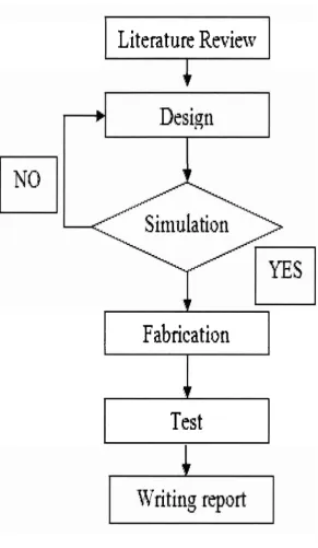
1.5 Methodology of Project
I
Literature Revie157
I
I
Fabrication
I
[image:23.527.135.427.65.567.2]Test
CHAPTER I1
LITERATURE REVIEW
2.1 Microstrip Antenna
2.1.1 Introduction