RECEPTION OF AUDIO AND VIDEO SIGNAL USING SQUARE WAVE FREQUENCY MODULATION
MOHD NAZREEN BIN ABDUL MAJID
This report is submitted in partial fulfillment of the requirements for the award of Bachelor of Electronic Engineering (Telecommunication Electronics) With Honours
Faculty of Electronic and Computer Engineering Universiti Teknikal Malaysia Melaka
UNIVERSTI TEKNIKAL MALAYSIA MELAKA
FAKULTI KEJURUTERAAN ELEKTRONIK DAN KEJURUTERAAN KOMPUTER
BORANG PENGESAHAN STATUS LAPORAN PROJEK SARJANA MUDA II
Tajuk Projek : RECEPTION OF AUDIO AND VIDEO SIGNAL USING SQUARE WAVE FREQUENCY MODULATION
Sesi
Pengajian : 2008 / 2009
Saya MOHD NAZREEN BIN ABDUL MAJID mengaku membenarkan Laporan Projek Sarjana Muda ini disimpan di Perpustakaan dengan syarat-syarat kegunaan seperti berikut:
1. Laporan adalah hakmilik Universiti Teknikal Malaysia Melaka.
2. Perpustakaan dibenarkan membuat salinan untuk tujuan pengajian sahaja.
3. Perpustakaan dibenarkan membuat salinan laporan ini sebagai bahan pertukaran antara institusi
pengajian tinggi.
4. Sila tandakan ( √ ) :
SULIT*
(Mengandungi maklumat yang berdarjah keselamatan atau kepentingan Malaysia seperti yang termaktub di dalam AKTA RAHSIA RASMI 1972)
TERHAD* (Mengandungi maklumat terhad yang telah ditentukan
oleh organisasi/badan di mana penyelidikan dijalankan)
TIDAK TERHAD
Disahkan oleh:
__________________________ ___________________________________ (TANDATANGAN PENULIS) (COP DAN TANDATANGAN
PENYELIA)
Alamat Tetap: ………...
………...
“I hereby declare that this report is the result of my own work except for quotes as cited in the references.”
Signature :...
“I hereby that I have read this report and in my opinion this report is sufficient in terms of scope and quality for the award of Bachelor of Electronic Engineering
(Telecommunication Electronics) with honours.”
Signature :... Supervisor’s Name : FAUZI BIN ABDUL WAHAB
ACKNOWLEDGEMENT
ABSTRACT
ABSTRAK
TABLE OF CONTENT
CHAPTER TITLE PAGE
PROJECT TITLE i
VERIFYING FORM ii
STUDENT DECLARATION iii
SUPERVISOR APPROVAL iv
DEDICATION v
ACKNOWLEDGEMENT vi
ABSTRACT vii
ABSTRAK viii
TABLE OF CONTENT ix
LIST OF TABLE xiii
LIST OF FIGURE xiv
LIST OF ABBREVIATION xv
I INTRODUCTION 1
1.1 Aplication Background 2
1.2 Project Objective 5
1.3 Problem Statement 6
1.4 Scope of Work 6
II LITERATURE REVIEW 9
2.1 Audio and Video 10
2.2 Modulation 11
2.2.1 Frequency Modulation 12
2.3 Phase Locked Loop 14
2.4 Square to Sine Wave Converter 15
2.5 Demultiplexing 15
2.4.1 Demultiplexer 16
2.6 Photodetector 17
2.7 Optical Fibre Communication 18
III PROJECT METHODOLOGY 20
3.1 Project Outline 21
3.2 Project Choosing 21
3.3 Project Planning 21
3.4 Literature Review 22
3.5 Circuit Design 22
3.6 Hardware Development 23
3.6.1 Development Process 24
3.6.1 Project Implementation 25
3.7 Multisim 10 26
3.8 Proteus 7 Professional 26
3.9 Measurement Process 26
3.10 Sub-circuit 26
3.10.1 Edge Triggered latches 27
3.10.2 Low Pass Filter 28
3.10.3 Band Pass Filter 29
IV RESULT & DISCUSSION 30
4.1 Introduction 31
4.2 Simulation 31
4.2.1 Optic Receiver 32
4.2.1 Video Receiver 33
4.2.1 Audio Receiver 34
4.3 Grapher 35
4.4 Measurement 38
4.4.1 Fibre Optic System 38
V DISCUSSION 41
5.1 Simulation 42
5.2 Fabrication Design 43
5.3 Systems Losses 44
5.4 Filter 45
5.4.1 Low Pass Filter 45
5.4.2 Band Pass Filter 45
5.5 Phase Locked Loop 46
VI CONCLUSION & SUGGESTION 47
6.1 Conclusion 48
6.2 Suggestion 49
REFERENCES 51
APPENDIX A 52
APPENDIX B 62
APPENDIX C 70
APPENDIX D 80
LIST OF TABLE
NO TITLE PAGE
4.1 Typical Value Of Attenuation 38
4.2 Power Level Measured From Power Meter 38
4.3 Parameter on Fibre Optic Systems 38
4.4 Power Margin for 1m & 3 m FO Cable 39
LIST OF FIGURE
NO TITLE PAGE
1.1 Schematic of an Optical Receiver 2
1.2 Receiver Sensitivity Curve 4
2.1 A Typical FM Signal Shown With the Modulating Signal 13
2.2 Frequency Synthesiser 14
3.1 Block Diagram of Receiver Systems 23
3.2 Design Process 24
3.3 Work Flow for Project Implementation 25
3.4 Positive Edge Triggered D-Latch Responses 27
3.5 Active Low Pass Filter 28
3.6 Passive Band Pass Filter 29
4.1 Optical Receiver Circuit without FO Connector 32
4.2 Video Receiver with 4.2M LPF 33
4.3 Audio Receivers with BPF 34
4.4 Simulation Results for Figure 4.1 35
4.5 Simulation Results for Figure 4.2 36
4.6 Simulation Results for Audio and Video Circuit 37
4.7 Fibre Losses in 1m FO Cable 39
LIST OF ABBREVIATION
AC - Alternating Current
AM - Amplitude Modulation
EMI - Electromagnetic Interference FDM - Frequency Division Multiplexing
FM - Frequency Modulation
IC - Integrated Circuit
MUX - Multiplexer
PAL - Phase Alternating Line
PM - Phase Modulation
SECAM - Sequential Colour with Memory SWFM - Square Wave Frequency Modulation TDM - Time Division Multiplexing
WDM - Wavelength Division Multiplexing BPF - Band Pass Filter
LPF - Low Pass Filter
APD - Avalanche Photodiode
PLL - Phase Locked Loop
VCO - Voltage Controlled Oscillator
CHAPTER I
INTRODUCTION
1.1 Application Background
The importance of communication systems can hardly be overestimated. Communication systems, such as TV, radio, fixed and mobile telephony, and the Internet, are essential in modern society. Efficient, rapid transmission of information reduces the need for energy-demanding transportation of paper and people, and can therefore reduce the negative impact on our common environment. Moreover, it is difficult to imagine a democratic society without efficient communication systems.
In the communication systems, there are transmitter and receiver. However, this research will only cover the receiver path where we will see the application of photo detector in optical receiver.
[image:17.612.182.477.471.643.2]Figure 1.1 shows a schematic of an optical receiver. The receiver serves two functions: It must sense or detect the light coupled out of the fiber-optic cable and convert the light into an electrical signal, and it must demodulate this light to determine the identity of the binary data that it represents. The receiver performs the OE transducer function.
The receiver schematic in Figure 1.1 shows a photodiode, bias resistor circuit, and a low-noise pre-amp. The output of the pre-amp is an electrical waveform version of the original information from the source.
To the right of this pre-amp are an additional amplification, filters, and equalizers. All of these components can be on a single integrated circuit, a hybrid, or discretely mounted on a printed circuit board.
There are two types of photodiode structures: positive intrinsic negative (PIN) and the avalanche photodiode (APD). In most premise applications, the PIN is the preferred element in the receiver. This is mainly due to fact that it can be operated from a standard power supply, typically between 5 and 15V.
APD devices have much better sensitivity. In fact, APD devices have 5 to 10 dB more sensitivity. They also have twice the bandwidth. However, they cannot be used on a 5V printed circuit board. They also require a stable power supply, which increases their cost. APD devices are usually found in long-haul communication links and can increasingly be found in metro-regional networks (because APDs have decreased in cost).
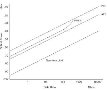
The demodulation performance of the receiver is characterized by the BER that it delivers to the user. The sensitivity curve indicates the minimum optical power that the receiver can detect compared to the data rate, to achieve a particular BER.
The quantum limit curve serves as a baseline reference. In a sense it represents optimum performance on the part of the photodiode in the receiver—that is, performance in which there is 100 percent efficiency in converting light from the fiber-optic cable into an electric current for demodulation. All other sensitivity curves are compared to the quantum limit
1.2 Project Objectives
The purpose of this project is to design a system for optical fibre reception of audio and video signal. It will be focusing on demodulation and separation of audio and video signal by using square wave frequency modulation.
The design of an optical receiver depends on the modulation format used by the transmitter. Since most light wave systems employ the binary intensity modulation, we will be focused on optical fibre receivers. We decided to implement and build a receiver for the reception of audio and video signal by using optical fibre as the transmission medium.
The main objectives that should be achieved at the end of this project are:
(a) To design system for optical fibre reception of audio and video signal. (b) To modulate square wave frequency modulation (SWFM).
1.3 Problem Statement
Transmission audio and video signal using copper cable has many disadvantages. There is undesired phase shift which can distort chrome information in long transmission lines. Possibility of ground loops and reflections can be result from improper termination of coaxial distribution systems.
Besides that, signal quality degradation is usually caused by inferior electromagnetic interference (EMI) of metal wire cable lines. EMI is electromagnetic energy that causes undesirable responses, degradation, or completes system failure.
1.4 Scope of Work
There are several areas that being identified or considered in order to maintain the progress due to the objective of this project:
(a) Studied on the square wave frequency modulation or digital communication systems and its operation.
This method is focusing on studying the basic digital systems that use the application of fibre optic cable itself.
(b) Analyzed digital modulation and demodulation techniques (SWFM)
(c) Application of Square to sine oscillator.
The digital application for this device, which that applied the process of generating the sine wave within the demodulation process.
(d) Filter application to normalised the signal
To differentiate the wave that transmitted to the receiver, this part will separate the signal to pull out the audio and video signal. The application of low pass filter and band pass filter take in charge in this process.
(e) Simulation the circuit by using the MULTISIM software
To sure the operational of the circuit, the simulation of the designed circuit is made before fabricating. From here we will troubleshoot any part of the circuit that seems to be affected of unwanted results.
(f) Design using PROTEUS 7 professional for PCB design
1.5 Methodology
There are several phases involved in order to achieve the objective of this project and achieved the optimum results:
(a) Project Planning (b) Literature Review (c) Hardware Construction (d) Finishing
CHAPTER II
LITERATURE REVIEW