World Applied Sciences Journal 22 (9): 1352-1354, 2013 ISSN 1818-4952
© IDOSI Publications, 2013
DOI: 10.5829/idosi.wasj.2013.22.09.365
Corresponding Author: Chee Fai Tan, Integrated Design Research Group (IdeA),
Faculty of Mechanical Engineering, Universiti Teknikal Malaysia Melaka, Melaka, Malaysia. Tel: +6062346710, Fax: +6062346884.
1352
Contaminants on Electrical Contacts Used in Semiconductor Device Testing
M.D. Radzai Said, K.Y. Ong and Chee Fai Tan
1 1 2
Faculty of Mechanical Engineering, Universiti Teknikal Malaysia Melaka, Melaka, Malaysia 1
Integrated Design Research Group (IDeA), Faculty of Mechanical Engineering, 1
Universiti Teknikal Malaysia Melaka, Melaka, Malaysia
Abstract:Electrical contacts used in semiconductor device testing are often deposited with a small pip of dark colour contaminants after being subjected to repeating cycles of impact loading. Samples of used electrical contacts are checked under SEM and EDX. It is discovered that the contaminants contain high percentage of tin elements. The reason as to why the contamination formed is investigated and it is found to be the result of material transfer from device lead. It is caused by the molten metal bridge formed when the contact begins to move apart.
Key words: Contaminants Electrical contacts Semiconductor
INTRODUCTION contacts [1]. Contact resistance (R ) is the sum of
In the industry of semiconductor device testing, the [2]. quality and lifespan of electrical contacts used is of
paramount importance because of high manufacturing R = R + R (1)
cost of electrical contacts used due to the demand of
small size and high precision. However, engineers are Constriction resistance itself is caused by the fact troubled with the fact that electrical contacts are always that real surfaces are not flat but comprise of small deposited with a pip of contaminant after a cycle of make asperities [2]. Hence, the conducting path of current is and break operation. Contaminants formed will affect the constricted to only a small fraction of the apparent accuracy of testing due to increasing contact resistance. contact area as illustrated in the following Figure 1. The conventional practice in the industry is to remove the Metal surface of electrical contacts are not clean contamination by either physical or chemical means. since oxides, sulfides, inorganic and organic compounds However, this could not be an ultimate solution because are present. These combine effect results in film resistance same accumulation of contaminants would occur [1].
again after cycles of impact loading. The removal of Hence, it is obvious that contact resistance would contaminants would also damage the surface of the rise when the contaminants accumalated on the electrical electrical contacts. To solve this problem, samples of contacts increases.
used electrical contacts and semiconductor devices are investigated under scanning electron microscope (SEM) and energy-dispersive X-ray spectroscopy (EDX) to determine the material composition of the contaminants and compared it with uncontaminated surface.
Contact Resistance: The contact resistance is the most Fig. 1: Constricted current flow causing constriction important and universal characteristic of electrical resistance (photo reprinted from [1])
c
constriction resistance (R ) and the resistance of film (R )s f
2
World Appl. Sci. J., 22 (9): 1352-1354, 2013
1353 Contact resistance is found to be a function of load applied to the electrical interface, hardness of the softer material and resistivity of the contact materials. Assume that the surface is clean of contaminants, contact resistance can be approximated as [3].
(2) If the upper and lower half of consist of different contact materials, contact resistance is derived as:
(3) where R is the contact resistance, c 1and 2 are resistivity of contact materials, H is the hardness of the softer material and F is the load applied to the electrical interface.
Investigation on Contaminant Using SEM/EDX: In order to identify the material composition of the contaminants and the nature of its formation, samples of used electrical contacts were taken from the industry and put under scanning electron microscope (SEM) and energy-dispersive X-ray spectroscopy (EDX). The samples used in this investigated are electrical contacts made of copper berrylium coated with gold. These contacts were previously subjected to impact loading by semiconductor leads made of copper coated with tin under the following conditions:
Contact load: 0.625N Contact time: 20ms Voltage: 5V
Number of cycles: 3.3 million
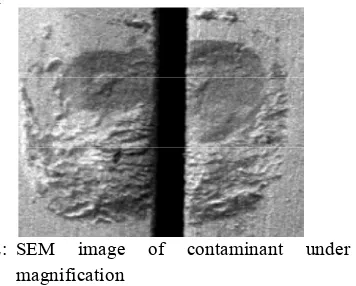
The following Figure 2 shows the SEM image of the contamination.
The dark grey part is the contaminants and the light grey part is the uncontaminated surface.
Fig. 2: SEM image of contaminant under 50X magnification
Fig. 3: EDX results of the contaminated surface
Table 1: Material composition of contaminated surface
Element Weight% Atomic%
Table 2: Material composition of uncontaminated surface
Element Weight% Atomic%
C 6.98 55.18
Au 93.02 44.82
Totals 100.00
As shown in Table 1, the contaminant comprise of high percentage of tin and oxygen. For comparison sake, the following Table 2 shows the material composition of uncontaminated surface.
The uncontaminated surface only contains the gold plating and some carbon.
DISCUSSION
Results reveal that the contaminant is of high tin content, oxygen elements represents the oxides, indicating that the contaminants contains metal oxides. Carbon elements exist on the surface may originated from the ambient air as studies by Rieder [4] did point out that ambient air is often contaminated with organic vapors. Organic vapors are obviously high carbon content. More than 300 organic vapors were identified in Skylab 4 [5].
The high tin content is obviously originated from the semiconductor device leads which are coated with tin. There are two possible theoretical explanations for the tin transfer from device leads to the electrical contact, namely adhesive wear and metal molten bridge.
m m
1 2
1/2 1/2
T T
1 1 2 2
T T
V=+2 dT 2 dT
∫
∫
World Appl. Sci. J., 22 (9): 1352-1354, 2013
1354
due to localized bonding between the contacting surfaces. electric arc. Further research needs to be carried out to When both bodies are pulled apart, material transfer take identify the physical factors that directly affect the net place from the cohesively weaker material (softer) to the mass or volume gain on the electrical contacts. Once the stronger material (harder) [1]. However, sliding motion are factors are determined, metallurgical solution can be minimum in impact motion and the only apparent cause of formulated.
friction is from the bouncing motion of electrical contacts.
Aside from that, tin (51MPa) is harder than gold (25MPa) REFERENCES
in Brinell scale. Also, from the SEM image, there is very
little sign of scratching, which indicates that there is not 1. Braunovic, M. and V. Konchits, 2006. Electrical much friction comes into play. Hence, it is highly unlikely Contacts: Fundamentals, Applications and that the high percentage of tin element found in the Technology. Florida: CRC Press.
contaminant pip results from adhesive wear. 2. Holm, R., 1979. Electrical Contacts. New York: Tin transfer from one surface to another can also Springer.
occur as a result of molten metal bridge. The physical 3. Timsit, R.S., 1999. Electrical Contact Resistance: explanation is given by Slade [6] which state that as the Fundamental Principles, in Electrical Contacts: contact begins to move apart, contact resitance increases Principles and Technology, pp: 12-46.
as the load on contact decreases as shown in Eq. 3. 4. Rieder, W. and G.J. Witter, 1999. Arc Interactions Voltage drop across the contact is given by: with Contaminants, in Electrical Contacts: Principles
V = IRc (4) 5. Bertsch, W., A. Zlatkis, H. Liebich, H. Schneider,
where V is the voltage drop, I is the current. Kohlrausch in skylab4. J. Chromatography, 99: 673-687. [3] derived a relationship between the voltage drop and 6. Slade, P.G., 1999. Electrical Contacts: Principles and
temperature as: Applications. New York: Marcel Dekker.
(5) investigations of the dynamic molter bridge, IEEE
where T is the maximum temperature, T and T is the bulkm 1 2 8. Slade, P.G. and M.D. Nahemow, 1971. Initial temperature, 1 and 2 are the electrical resistivity of separation of electrical contacts carrying high contact materials and 1 and 2 are the thermal currents, J. Applied Physics, 42(9): 3290-3297. conductivities of contact materials. 9. Koren, P.P. and M.F. Hoyaux, 1975. The effect of
As the contact force slowly decreases when the electrode material on the initial expansion of an arc in contact parts, temperature of the contact spot will reach vacuum. IEEE Trans Parts Hybrids Packaging, PHP-8, the melting point of the metal. Once the contact spot has pp: 35-47.
metled and the contacts continue to part, a molten bridge 10. Unigraphics User Menual Version 13, 1997 is drawn between them [6]. Holm [2] confirmed that molten (Electronic Data System Corporation, Unigraphics metal bridge always form between the contacts even at Division, MO USA).
low currents [2]. Studies by Utsumi [7], Slade [8] and 11. Sunil, V.B. and S.S. Pande, 2008. Automatic Koren [9] also prove that molten bridge can form when Recognition of Features from Freeform Surface CAD contact open with high acceleration. As the bridge is Models. Computer-Aided Design, 40(4): 502-517. drawn further, it will rupture. The rupture of the bridge will 12. Ran, J.Q. and M.W. Fu, 2010. Design of Internal Pins followed by arc formation and eventually results in in Injection Mold CAD via the Automatic accumulation of material on the cathode. Recognition of Undercut Features. Computer-Aided
CONCLUSION 13. De Martino, T., B. Falcidieno and F. Giannini, 1994. From the SEM images and EDX results, it can be Machining Contexts. Advances in Engineering concluded that the contamination is primarily caused by Software, 20(2-3): 91-105.
net material transfer as a result of molten metal bridge and
and Technology, pp: 810.
1974. Concentration and analysis of organic volatiles
7. Utsumi, T., 1969. Theoretical and experimental Trans Parts, Materials and Packaging, PMP-5(1), pp: 62-68.
Design, 42(7): 582-597.