Australian Journal of Basic and Applied Sciences
ISSN:1991-8178Journal home page: www.ajbasweb.com
Corresponding Author: H.H.M.Yusof, Lecturer in Industrial Electronics Department, Universiti Teknikal Malaysia
Melaka, Malaysia.
E-mail: [email protected]
Compatibility Analysis of Silicon Nitride and Silicon Dioxide on HCI induced LDD MOSFET
1
H.H.M. Yusof, 2N. Soin, 3Nissar M. K., 4M. Sufyan, 5Faiz Arith
1Department of Industrial Electronics, Faculty of Electronics and Computer Engineering, Universiti Teknikal Malaysia Melaka, Hang Tuah
Jaya, 76100 Durian Tunggal, Melaka, Malaysia.
2Department of Electrical Engineering, Faculty of Engineering, University of Malaya, 50603Kuala Lumpur, Malaysia. 3
Department of Electrical Engineering, Faculty of Engineering, University of Malaya, 50603Kuala Lumpur, Malaysia.
4
Department of Electrical Engineering, Faculty of Engineering, University of Malaya, 50603Kuala Lumpur, Malaysia.
5Department of Computer Engineering, Faculty of Electronics and Computer Engineering, Universiti Teknikal Malaysia Melaka, Hang
Tuah Jaya, 76100 Durian Tunggal, Melaka, Malaysia.
A R T I C L E I N F O A B S T R A C T
Background: Hot-carrier-injection (HCI) is one of important reliability issue under short-channel effect in modern MOSFET devices especially in nano-scaled CMOS technology circuits. The effect of the hot carrier can be reduced by introducing Lightly-Doped-Drain (LDD) structure on the device. The objective of this project is to study the effect of hot carrier in the LDD n-MOSFET. The LDD n-MOSFET is stressed with bias voltage at intervals of stressing time to determine the degradation model in the threshold voltage and drain current. From the parametrical analysis, it shows that the shift in threshold voltage and degradation in the drain current occurred after the MOSFET device is stressed with hot carrier stress test. The rate of threshold voltage shift and degradation of the drain current are dependence to the stressing time applied to the MOSFET device. The hot carrier stress test shows that the device with Si3N4 has
smaller voltage shift compared to SiO2 material.
© 2014 AENSI Publisher All rights reserved. To Cite This Article: H.H.M. Yusof, N. Soin, Nissar M. K., M. Sufyan and Faiz Arith, Compatibility Analysis of Silicon Nitride and Silicon Dioxide on HCI induced LDD MOSFET. Aust. J. Basic & Appl. Sci., 8(16): 25-33, 2014
INTRODUCTION
Since the invention of CMOS technology, the dimensions of the electronic devices are shrinking day by day. The demand for small area and low power are the main reasons behind the miniaturization of CMOS transistor up to nano level. The higher number of transistors is required in order to produce higher performance chip at smaller packaging size (Faiz, A. et al.,2013) (Idzdihar, M.I. et al., 2012). As transistor size is shrinking, many reliability issues have been raised as critical constraints which adversely affect the performance of a system. Since the evolution of CMOS miniaturization technology, Hot Carrier Injection (HCI) has been raised as one of the critical issues. This problem occur due to the aggressive scaling of transistors in nano-scale which cause the high electrical field at drain region, therefore HCI instability takes place in the n-channel MOSFETs which leads to the degradation of device performance. Since the key factor of hot carrier generation is due to high electric field at the drain, the hot carrier effect can be minimized by reducing the electric field strength at the channel (An, H. et al., 2013) (Bae, J. et al., 2009). The purpose of reducing the electric field strength at the drain is to separate the maximum current path away from the maximum electric field. This can be done by introducing the lightly-doped-drain (LDD) structure on MOSFET devices.
The LDD structure is used to separate out the strong electric field between heavily doped drain/source and channel [5]. High k dielectric is necessary to reduce the leakage current but Ta2O5, Al2O3, La2O3, ZrO2, HfO2 (Yoshio, O. and P. J. Tobin, 1994) (Polishchuk, I. et al., 2001) (Park, D. et al., 1998) (Chin, A. et al., 2000) (Ma, Y. et al., 1999) (Klang, L. et al., 2000) and many other silicates have problems with sustainability of the device. Si3N4 also can be used in this study since it has higher relative dielectric constant compared to SiO2 (Lu, Q., 1999).
(1)
which shows that where,
(2)
It has been explained that the distribution of the lateral electric field in LDD-MOSFETs is different if compared to conventional MOSFET devices (Muhammad, M. et al., 2009). Silver nitride has been used as the spacer for the LDD MOSFET in the past but it causes the large degradation. It has been found that this degradation is due to the HCI effect in the side-wall spacer of LDD MOSFET (Tomohisa M. et al., 2010). The main objective of this paper is to study the HCI effect on sub-nanometer LDD n-MOSFET and its impact on the threshold voltage VTH and drain current ID for two oxide materials, SiO2 and Si3N4.
Experimental Design:
TCAD device simulator is used to virtually fabricate the implemented device and device electrical characterizations on the hot carrier analysis. First, the device is virtually fabricated by using Silvaco ATHENA software. In order to check the electrical behavior, Silvaco ATLAS software is used to characterize the basic electrical information such as threshold voltage and drain current of the structural created by ATHENA. Besides that, the hot carrier stress test is also done by using this software where the device is stressed with stressing condition to obtain the electrical parameter degradation due to hot carrier effect. By using this software, all the aspect of device simulation can be characterized not only for CMOS technology but with wide range of integrated circuit design application (Muzalifah, M. S. et al., 2013). Geometrical dimensions and process parameters of the device are shown in Table 1.
The substrate of LDD n-MOSFET was developed by starting with initial silicon in 2D <100> orientation and boron impurities. The gate oxide was growth by depositing the oxide with specified thickness of 2 nm. Threshold voltage was then implanted by depositing boron and poly-silicon gate is deposited on oxide. LDD structure having light doping concentration was implanted with phosphorus at concentration of 4 x 1013 cm-3. To secure the LDD area before doing the source/drain channel high doped implant, spacer oxide sidewall was created. At this point, the source/drain can now be implanted with arsenic having high dose of 2 x 1016 cm-3. Oxide layer is still remaining on the structure at this point. Aluminium needs to be deposited as a contact for source and drain. The oxide layer needs to be etched first before depositing the aluminium layer. Fig. 1 shows the cross section of full structure of LDD n-MOSFET in which the parameters and dimensions have been taken from Table 1.
Table 1: Process parameters of the device
Geometrical Dimension Process Parameter Material / Impurities Value
Device Length - 1.2 µm
The LDD n-MOSFET structure was loaded into the simulation file followed by the simulation model. The characterization was first done based on the default structure at default bias condition without stressing time. This purposely is to make the comparison in the graph between non-stressed behaviour and stressed behaviour. After non-stressed characteristic was done, the device is now stressed at bias condition at interval period. These stress conditions were based on the default temperature condition which is at 300 K. Table 2 shows the stressed biased conditions for the simulation (Chen, C. et al, 2001).
Fig. 1: Full LDD n-MOSFET structure
Table 2: Stressed biased conditions
Stress Condition Value
Gate Voltage 0.2553 V
Drain Voltage 2.5 V
Time 10 s, 30 s, 100 s, 300 s, 1000 s
Temperature 300K
RESULTS AND DISCUSSION
Comparison of Threshold Voltage between Si3N4 and SiO2:
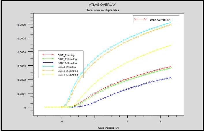
Fig. 2 shows the ID versus VG curves for Si3N4 and SiO2 across the oxide thickness of 2 nm, 2.5 nm and 5.9 nm. The graph shows that Si3N4 the material has lower threshold voltage compared to SiO2 across all the oxide thickness. From the result, the higher dielectric constant produced lower threshold voltage. It is also shows that the thicker the dielectric the higher the threshold voltage level.
From the data in Fig. 3 and Table 3, the percentage of the threshold voltage different between SiO2 and Si3N4 is 76% for 2 nm, 77% for 2.5 nm and 54% for 5.9 nm thickness of oxide. This is shows that the higher the dielectric constant the lower the threshold voltage.
Fig. 3: VTH versus tox - Comparison between SiO2 and Si3N4 dielectric material across thickness.
Table 3: Comparison on threshold voltage between SiO2 and Si3N4 dielectric material across thickness.
Tox (nm) VTH (V)
SiO2
VTH (V)
Si3N4 ∆VTH (V) ∆VTH (%)
2 0.2553 0.0625 0.1928 76%
2.5 0.2939 0.0688 0.2251 77%
5.9 0.5478 0.2525 0.2953 54%
Comparison of Drain Current between Si3N4 and SiO2:
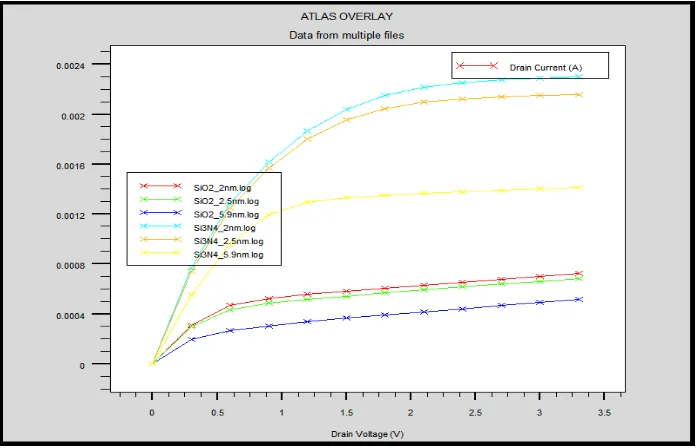
Fig. 4 shows the ID versus VD curves for Si3N4 and SiO2 across the oxide thickness of 2 nm, 2.5 nm and 5.9 nm. The graph shows that the material of Si3N4 produced higher drain current compared to SiO2 material. The trends are same for all the oxide thickness size. By comparing side by side, for all 2 nm, 2.5 nm and 5.9 nm thicknesses had shown the similar behavior which is reduction in drain current.
Fig. 4: ID versus VG – Comparison between SiO2 and Si3N4 dielectric material across thickness.
thickness, the drain current value for Si3N4 is reduced about 219% compared to SiO2 material. The 2.5 nm and 5.9 nm oxide thicknesses also experienced the same behaviour where the reductions of the drain current are 216% and 175% respectively.
Fig. 5: ID versus tox – Comparison between SiO2 and Si3N4 dielectric material across thickness.
Table 4: Comparison on drain current between SiO2 and Si3N4 dielectric material across thickness.
Tox (nm) ID (A)
SiO2
ID (A)
Si3N4 ∆ID
(A) ∆ID (%)
2 0.00072 0.00230 0.00158 219%
2.5 0.00068 0.00216 0.00148 216%
5.9 0.00051 0.00141 0.00090 175%
Hot Carrier Injection (HCI) a nalysis on LDD nMOSFET:
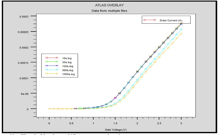
Fig. 6 shows that the threshold voltage was shifted to right side which means in incremental value across the stressing time. The threshold voltage shift can cause a delay in operating frequency (Fakhruddin, M. et al., 2007).
Fig. 6: ID versus VG - Threshold voltage shift across stressing time
subsequent shift between the stressing time were considered small with the highest shift with reference to initial condition was at 1000 s stressing time.
Fig. 7: VTH versus stress time.
Table 5: Threshold voltage shift data.
Stress Time (s) VTH (V) ∆VTH (V) ∆VTH (%)
0 0.2553 Reference
10 0.8250 0.5697 223%
30 0.8254 0.5701 223%
100 0.8273 0.5720 224%
300 0.9825 0.7273 285%
1000 1.0072 0.7519 295%
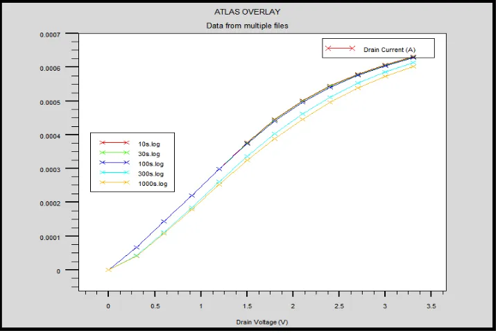
The drain current characteristic during hot carrier effect is shown in Fig. 8. The ID versus VD curve was taken at VG = 2.2 V for all the stressing time and the curve shows the drain currents were slightly reduced at every setting of stressing time.
Fig. 8: ID versus VD – Drain current degradation.
The drain current shift about 12.55% from non-stress condition to stressed condition at 10 s. This is about 0.0906 mA reduction in drain current. The highest reduction of drain current is at 1000 s stressing time where the reduction is about 0.1207 mA or 16.72%. This proved that the relationship between the shift of threshold voltage and drain current graph. The degradation of drain current between 10 s and 1000 s is considered small.
Fig. 9: ID versus stress time.
Table 6: Drain current degradation data.
Stress Time (s) ID (A) ∆ID (A) ∆ID (%)
0 7.222E-04 Reference
10 6.316E-04 9.061E-05 12.55%
30 6.308E-04 9.138E-05 12.65%
100 6.283E-04 9.388E-05 13.00%
300 6.136E-04 1.086E-04 15.04%
1000 6.015E-04 1.207E-04 16.72%
Comparison of HCI between SiO2 and Si3N4 Dielectric Material:
For the comparison on hot carrier stress test between oxide materials, the materials that used are silicon dioxide, SiO2 and silicon nitride, Si3N4. The comparison is purposely to see the degradation trend between these two materials. As presented before, the threshold voltage for Si3N4 is lower compare to SiO2 due to high dielectric constant on Si3N4 material. Therefore, the value of threshold voltage for Si3N4 is lower in this simulation.
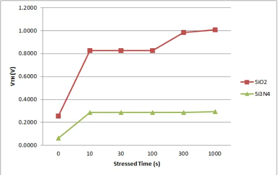
Fig. 10 shows the comparison graph for both materials. Material Si3N4 shows the shift of threshold voltage at 10 s but for the rest of stressing time it looks like similar. By looking at the result data in Table 7, the threshold voltage shift for Si3N4 material is very small after 10 s stress. This shows that the device with Si3N4 has smaller voltage shift at 10 s and more stable at longer stress time compared to SiO2 material.
Table 7: Threshold voltage shift data for SiO2 versus Si3N4.
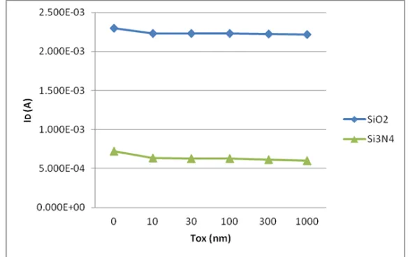
Fig. 11 and data in Table 8 show that the drain current degradation is very small for Si3N4 material. This is due to the very small shift in threshold voltage for Si3N4 material. The shift of threshold voltage is less than 1 mV for between stressing times, therefore the drain current degradation is also very small which is less than 10 µA.
Fig. 11: ID versus stress time – Comparison between SiO2 and Si3N4
Table 8: Drain current degradation data for SiO2 versus Si3N4.
Stress Time (s) ID (A)
A study of the electrical characteristics and hot carrier degradation of LDD n-MOSFET has been presented in this paper. The device electrical characteristics across the process parameter such as oxide thickness and oxide material were analyzed by determining the threshold voltage and the effect on the drain current. Si3N4 oxide material produced lower threshold voltage compared to SiO2 oxide material. The higher threshold voltage produced lower drain current value vice versa. This is because of the drain current is proportional with VG - VTH where the higher VTH results lower value of VG - VTH. The hot carrier stress test was carried out on default structure. In addition, the devices with different oxide materials were also simulated with hot carrier stress test. The hot carrier stress test shows that the device with Si3N4 has smaller voltage shift at 10 s and more stable at longer stress time compared to SiO2 material.
ACKNOWLEDGEMENT
This research is financially supported by the university under PJP grant scheme (No: PJP/2013/FKEKK(31B)/S01221).
REFERENCES
Bae, J., E.L. Shim, T.Y. Park, C.J. Kang and Y.J. Choi, 2009. Formation of ZnO nanocones using wet chemical etching of ZnO nanorods in an aqueous solution of HCI. Journal of Nanoscience and Nanotechnology, 9(12): 7398-7401.
Chen, C.K., C.L. Chen, P.W. Gouker, P.W. Wyatt, D.R. Yost, J.A. Burns, V. Suntharalingam, M. Fritze and L. Keast, 2001. Fabrication of self-aligned 90-nm fully depleted SOI CMOS SLOTFETs. IEEE Electron Device Letters, 22(7): 345-347.
Chin, A., Y. Wu, S. Chen, C. Liao and W. Chen, 2000. High quality La2O3 and Al2O3 gate dielectrics with equivalent oxide thickness 5-10Å. Symp. on VLSI Technology Digest of Technical Papers, 2(4): 16-17.
Faiz, A., M. Mamun, M.A.S. Bhuiyan and A.A.A. Bakar, 2013. Low voltage schmitt trigger in 0.18µm CMOS technology. Advances. in Natural Applied Sciences, 7(1): 33-38.
Fakhruddin, M., T. Mao Chyuan, J. Kuo, J. Karp, D. Chen, C.S. Yeh and S.C. Chien, 2007. Hot Carrier Degradation and Performance of 65nm RF n-MOSFET. In Radio Frequency Integrated Circuits (RFIC) Symposium, 2007 IEEE, pp: 551-554.
Idzdihar, M.I., M.N.S. Zainudin, M.M. Ismail and R.A. Rahim, 2012. Design of a Low Voltage Class AB Variable Gain Amplifier (VGA). Journal of Telecommunication, Electronic and Computer Engineering, 4(2): 69-74.
Klang, L., Y. Jeon, K. Onishi, B.H. Lee, W.J. Qi, R. Nieh, S. Gopalan and J.C. Lee, 2000. Single-layer thin HfO2 gate dielectric with n+ polysilicon gate. Symp. on VLSI Technology Digest of Technical Papers, 5(3): 44-45.
Lu, Q., 1999. Comparison of 14Å TOX, EQ JVD and RTCVD silicon nitride gate dielectrics for sub-100 nm MOSFETs. Int. Semiconductor Device Research Symp. 489.
Ma, Y., Y. Ono, L. Stecker, D.R. Evans and S.T. Hsu, 1999. Zicronium oxide based gate dielectrics with equivalent oxide thickness of less than 1.0 nm and performance of submicron MOSFET using a nitride gate replacement process. Int. Electron Devices Meeting Tech. Dig., pp: 149-152.
Muhamad, M., S. Lokman and H. Hussin, 2009. Optimization in fabricating 90nm NMOS transistors using Silvaco. IEEE Student Conference on Research and Development (SCOReD), pp: 258-261.
Muzalifah, M.S., Z.A. Fauzan, F. Arith and M.N. Zarina, 2013. NMOS performance of low boron activation on group v for ultra shallow junction formation. Advanced Materials Research, 716: 248-253.
Park, D.Y., C. King, Q. Lu, T.J. King, C. Hu, A. Kalnitsky, S.P. Tay and C.C. Cheng, 1998. Transistor characteristics with Ta2O5 gate dielectric. IEEE Electron Device Letters, 19(11): 411.
Polishchuk, I., Y.C. Yeo, Q. Lu, T.J. King and C. Hu, 2001. Hot-Carrier Reliability Comparison for pMOSFETs With Ultrathin Silicon-Nitride and Silicon-Oxide Gate Dielectrics. IEEE Transactions on Device and Materials Reliability, 1(3): 158-162.
Pomper, M., W. Biefuss, K. Horinger and W. Kaschite, 1982. A 32-bit execution unit in an advanced nMOS technology. IEEE Journal of Solid-State Circuits, 17(3): 50-53.
Tomohisa, M., S. Sawada, Y. Saitoh and S. Shinozaki, 2010. Si3N4/SiO2 Spacer Induced High Reliability in LDDMOSFET and its Simple Degradation Model. Semiconductor Device Engineering Laboratory.