International Journal of Science and Engineering Applications Volume 3 Issue 2, 2014, ISSN-2319-7560 (Online)
www.ijsea.com 6
OPTICAL SWITCHING CONTROLLER USING FPGA AS A
CONTROLLER FOR OCDMA ENCODER SYSTEM
Jaafar, A.
Faculty of Electronic and Computer
Engineering
Universiti Teknikal Malaysia
Melaka (UTeM)
Hang Tuah Jaya, 76100 Durian
Tunggal,Melaka, Malaysia
Saffie, N.B.
Faculty of Electronic and Computer
Engineering
Universiti Teknikal Malaysia
Melaka (UTeM)
Hang Tuah Jaya, 76100 Durian
Tunggal,Melaka, Malaysia
M.H. Sulaiman
Faculty of Electronic and Computer
Engineering
Universiti Teknikal Malaysia
Melaka (UTeM)
Hang Tuah Jaya, 76100 Durian
Tunggal,Melaka, Malaysia
Abstract: This paper proposed a design of optical switching controller using FPGA for OCDMA encoder system. The encoder is one of the new technologies that use to transmit the coded data in the optical communication system by using FPGA and optical switches. It is providing a high security for data transmission due to all data will be transmitting in binary code form. The output signals from FPGA are coded with a binary code that given to an optical switch before it signal modulate with the carrier and transmit to the receiver. In this paper, AA and 55 data were used for source 1 and source 2. It is generated sample data and sent packet data to the FPGA and stored it into RAM. The simulation results have done by using software Verilog Spartan 2 programming to simulate. After that the output will produces at waveform to display the output. The main function of FPGA controlling unit is producing single pulse and configuring optical switching system.
Keywords: Field programmable gate array (FPGA), Code Division Multiple Access (CDMA), Optical Code Division Multiple Access (OCDMA), Linear Feedback Shift Register (LFSR), pseudo-noise (PN), Verilog
1.
INTRODUCTION
Interest in OCDMA has been steadily growing during recent decades. That trend is accelerating due to fiber penetration in the first mile and the establishment of PON technology as a pragmatic solution for residential access. OCDMA is one promising technique for next-generation broadband access network with the following advantages: asynchronous access capability, accurate time of arrival measurements, and flexibility of user allocation, ability to support variable bit rate, busty traffic and security against unauthorized users. OCDMA is a very attractive multi-access technique that can be used for local area network (LAN) and the first one mile. Moreover, the OCDMA method is preferable for multiplexing in the optical domain because it uses broadband widths in optical devices for the electrical CDMA method and the electrical-to-optical (E/O) conversion OCDM is a multiplexing procedure by which each communication channel is distinguished by a specific optical code rather than a wavelength or time-slot[11]. An encoding operation optically transforms each data bit before transmission. At the receiver, the reverse decoding operation is required to recover the original data. OCDMA is the use of OCDM technology to arbitrate channel access among multiple network nodes in a distributed fashion. There are many different kinds of OCDMA encoder/decoders use optical delay lines or optical switches with optical orthogonal code (OOC) for the time domain fiber Bragg grating (FBG) or AWGs and OOCs for the optical frequency domain, and FBGs or AWGs for optical wavelength-hopping / time spreading (TS)[4]. AWG-based encoder/decoder has the unique capability of simultaneously processing multiple time-spreading optical codes (OCs) with single device, which makes it a potential cost-effective device to be used in the central office of OCDMA network to reduce the number of encoder/decoders. The AWG-based encoder/decoder also has very high power contrast ratio
(PCR) (15~20 dB) between auto- and cross-correlation signals, which means the interference value could be significantly reduced (up to 20 dB) with the short OC [1-3].
International Journal of Science and Engineering Applications Volume 3 Issue 2, 2014, ISSN-2319-7560 (Online)
www.ijsea.com 7
Optical systems are mainly intensity modulated and hence the chips in the OCDMA system are alternating '1' s and '0' s instead of '-1' s and '+1' s. In OCDMA the overlap of optical pulses results in the addition of optical power. Optimum CDMA codes have been found assuming bipolar signals which can take on positive and negative values, though optical signal can also be processed coherently to provide bipolar signals. Recently practical optical fiber systems use direct detection and can therefore process only unipolar signals consisting of "1" s and "0" s. CDMA codes consisting entirely of '1' s and '0' s are referred to as optical codes and several variants have been recently proposed in many literature. An important class of CDMA optical codes is so called set of OOCs (Orthogonal Optical Codes)[5]. OOC is a family of (0,1) sequences with good auto and cross correlation properties. The (1,0) sequences of OOC are called its code words. In other words, the cross -correlation of two distinct CDMA codes must take a value as low as possible.
Field Programmable Gate Arrays (FPGAs) are programmable semiconductor devices that are based around a matrix of Configurable Logic Blocks (CLBs) connected through programmable interconnects. Verilog HDL is one of the two most common Hardware Description Language (HDL) used by integrated circuit (IC) designers. The other one is VDHL[6]. HDL’s allows the design to be simulated earlier in the design cycle in order to correct errors or experiment with different architectures. Design describes in HDL are technology independent, easy to design and simulate and are usually more readable than schematics normally for the large circuits. Verilog can be used to describe designs at four levels of abstraction which is algorithms level (much like c code with if, case and loop statements). Register transfer level (RTL uses registers connected by Boolean equations). Gate level (interconnected AND, NOR etc). switch level (the switches are MOS transistors inside gates). The language also defines construct that can used to simulate the input and output. Mostly, Verilog is used as an input for synthesis programs and will generate a gate level description and analyze for the coding. Some Verilog construct are not synthesizable. The code is written will greatly affect the size and speed of the synthesize. Normally, the readers want to synthesize their coding, so non synthesizable construct should be used only for test benches [12-14].
2.
OVERVIEW SYSTEM
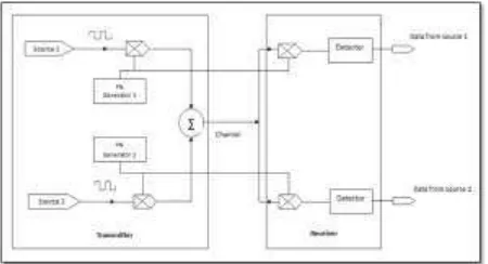
Figure 1 shows the operation of Code Division Multiple Access process. At the transmitter, two data sources generated digital data sequences which are individually multiplied using two orthogonal code sequences. Both of data user is identified by its unique code. The serial data sequences are multiplied by their corresponding PN sequences. The PN code sequence can be easily generated using Linear Feedback Shift Register (LFSR). The orthogonal code sequences are generated by periodically repeating orthogonal codes are at a rate much greater than the source data rate. The modulated sequence has wider frequency spectrum more than the original source sequence. It is called spread spectrum data sequence. The two spread spectrum data sequences are finally summed up and transmitted over a common channel.
Figure 1: Block Diagram of Code Division Multiple Access
2.1
pseudo-noise(PN) Generator Operation
This operation consist 7-bit PN code generator by using three stages Linear Feedback Shift Register (LFSR). The logic circuit diagram of three stage LFSR implement in Verilog coding is shown in figure above. This operation of three stage of LFSR used D flip flop gate. PN generators are separated by two parts, which entities were implemented, one of each for two sources. The 3-bit initialize (seed) was set within the Verilog coding itself for each entity. The PN generator for source 1 is initialized with (S2 S1 S0) = 110. This input are generates PN code 1100101. For PN generator for source 2 is initialized with (S2 S1 S0) = 111. This input are generates PN code 1110010. The operation of PN generator by using three stages LFSR shows at figure 2 below. The PN generator components generate the respective PN sequences for two sources. To ensure that seven chips in the PN sequence align exactly with one bit of serial data, the PN sequence is generated at the master clock rate example master clock rate is assumed to be 7x. The serial data sequence is generated at one seven rate of master clock. This operation also used XOR gate.
Figure 2: Three stage of LFSR
2.2
Linear Feedback Shift Register (LFSR)
The PN generator for spread spectrum is usually implemented as a circuit consisting of exclusive OR gates and a shift register, called a Liner Feedback Shift Register (LFSR)[7-8]. The LFSR is a string of 1-bit storage devices. Each device has an output line, which indicates the value currently stored, and an input line. At discrete time instants, known as clock times, the value in the storage device is replaced by the value indicated by its input line. The entire LFSR is clocked simultaneously, causing a 1-bit shift along the entire register.
2.3
Data Source
International Journal of Science and Engineering Applications Volume 3 Issue 2, 2014, ISSN-2319-7560 (Online)
www.ijsea.com 8
clock rate and the output bit changes every 7th master clock cycle. The serial output is synchronized with PN sequence such that one data bit period equals seven PN code chips.
2.4
Channel
Channel is the medium through which the signals are transmitted by using fiber optic cable [7]. A communication channel can be generally characterized as liner filters and signals transmitted over the channel suffer distortion due to channel response and noise. In CDMA, since all user channels operate simultaneously in the same RF band, the interference due to the multiple users in same RF channel become more important factor and it plays vital role in deciding the performance of the communication system. A mobile channel includes effects of multipath fading and noise. In the simulation however, only Additive White Gaussian Noise (AWGN) channel has been used, which is the simplest channel models, from analysis point of view. A built in command awgn() was used to model AWGN channel.
In the simulation communication link has been modeled as a forward channel where each user data is uniquely identified and spread using Walsh codes. As mentioned earlier, the perfect orthogonality of Walsh codes significantly reduces the probability of error at receiver. In order to simulate bit errors due to multipath effect, intercellular interferers, random non orthogonal data were added onto the AWGN channel. These interfering signals are not orthogonal with the Walsh codes used for the channels in the concerned cell and thus causes substantial amount of error. However in order to simulate error due to the multipath interferences from the users operating in the same cell or the interferences coming from users in other cells, random data was added in the channel that may not be exactly orthogonal to the Walsh codes. At PN generator operation use three stages Linear Feedback Shift Register (LFSR). Whereby use three gate XOR to shift the binary code.
3.
EXPERIMENTAL RESULTS
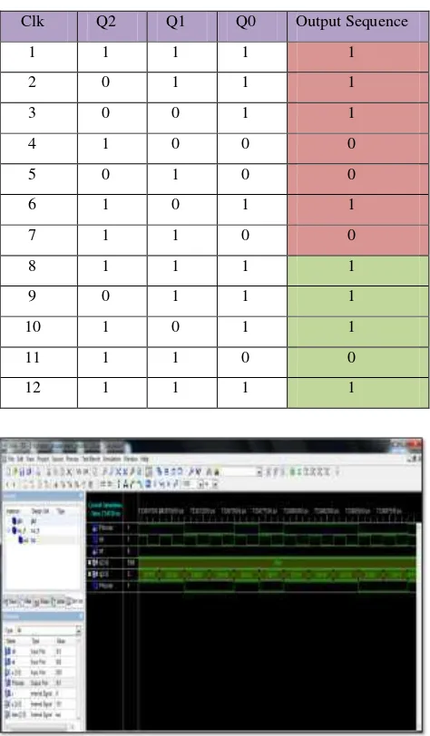
At the PN Generator process, we need to use the three stages LFSR to generate the output data. Input 110 seed to PN Generator and will shift using three stages of LFSR used XOR gate. The output after process shows in table 1 below.
Input 110 = Output 1100101
Table 1. PN generator for input 110
Figure 3: Simulation result for PN generator 110
At the PN Generator process, we need to use the three stages LFSR to generate the output data. Input 111 seed to PN Generator and will shift using three stages of LFSR used XOR gate. The output after process shows in table 2 below.
Input 111 = Output 1110010
Table 2. PN generator for input 111
Clk Q2 Q1 Q0 Output Sequence
1 1 1 1 1
2 0 1 1 1
3 0 0 1 1
4 1 0 0 0
5 0 1 0 0
6 1 0 1 1
7 1 1 0 0
8 1 1 1 1
9 0 1 1 1
10 1 0 1 1
11 1 1 0 0
12 1 1 1 1
Figure 4: Simulation result for coding 111 Clk Q2 Q1 Q0 Output Sequence
1 0 1 1 1
2 0 0 1 1
3 1 0 0 0
4 0 1 0 0
5 1 0 1 1
6 1 1 0 0
7 1 1 1 1
8 0 1 1 1
9 0 0 1 1
10 1 0 0 0
11 0 1 0 0
International Journal of Science and Engineering Applications Volume 3 Issue 2, 2014, ISSN-2319-7560 (Online)
www.ijsea.com 9
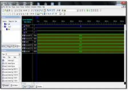
The final output for transmitted data encoder can prove from calculation.
Input from data 1 was set as AA for encoder 0
Encoder 0 = AA + PN code 110
= 10101010 + 1100101
= 1OF [Eqn 1]
Input from data 2 was set as 55 for encoder 1
Encoder 1 = 55 + PN code 111
= 1010101 + 1110010
= C7 [Eqn 2]
Encoder final = Encoder 0 + Encoder 1
= 10F + C7
= 1D6 [Eqn 3]
Figure 5: Simulation result for final encoder (Transmit) Figure 5 above shows the simulation result for final encoder (transmitted) data using FPGA as a controller. The simulation result has shown at figure above. After running simulation complete, the result for encoder 0 is 1OF and for encoder 1 is C7. For final encoder the data transmit is 1D6. The output is 8 bit and show in hex code. The value of 1 is carry flag.
4.
CONCLUSION
This paper was carried out two major objectives of implementing a CDMA system at simulating a CDMA communication system in Verilog. The first objective was successfully developed and for the second objective was successfully accomplished after extensive designing, coding and testing. A two users CDMA system was implemented in Verilog and synthesized onto an FPGA board. The operation of the system was successfully verified. The various PN Generator topologies were studied and they were synthesized using Xilinx ISE software. Device Utilization and No of Logic Blocks of each topology were noted down and compared with each other. The simulations have done by using Verilog code.
5.
ACKNOWLEDGMENTS
This research is funded by the grant from Faculty of Electronic and Computer Engineering, Universiti Teknikal Malaysia Melaka (UTeM) with project number of PJP/2013/FKEKK(47B)/S01274.
6.
REFERENCES
[1] Harold P.E. Stern, Samy A. Mahmoud, “Theory of Code Division Multiplexing, Communication Systems: Analysis and Design”, Prentice Hall PTR.
[2] Y. Wang, et al., "Design and experiment of an all-optical label using FBG-based encoder/decoders," 2009, pp. 727811-1.
[3] M. S. Ab-Rahman, et al., "Development of Low-cost OCDMA Encoder based on Arrayed Waveguide Gratings (AWGs) and Optical Switches," World Academy of Science, Engineering and Technology, vol. 46, 2008.
[4] Shah, “Code DivisionMultiple Access : A Tutorial”, p6-10,Wireless Communication, Rowan University,1999.
[5] C. Zhang, et al., "Experimental demonstration of tunable multiple optical orthogonal codes sequences-based optical label for optical packets switching," Optics Communications, vol. 283, pp. 932-938, 2010.
[6] B. Zeidman and Z. Consulting, Introduction to verilog: IEEE Press, 2000.
[7] K. Skahill, “VHDL for Programmable Logic”, Addison -Wesley,1999.
[8] A. Dhital, "CDMA System: Simulation and Implementation," 2006.
[9] S. Prakash, et al., "Compact field programmable gate array (FPGA) controller for aircraft/aerospace structures," 2008.
[10]M. Akiyama, et al., "High-performance pulsed-power generator controlled by FPGA," Plasma Science, IEEE Transactions on, vol. 38, pp. 2588-2592, 2010.
[11]M. Zainudin, H. Radi, and S. Abdullah, “Face
Recognition using Principle Component Analysis (PCA) and Linear Discriminant Analysis (LDA),” ijens.org, no. 05, 2012.
[12]A. Jaafar, N. Arasid, N. Hashim, A. Latiff, and H. Rafis, “Three Bit Subtraction Circuit via Field Programmable Gate Array,” ijaret.org, vol. 1, no. Viii, pp. 1–13, 2013. [13]Jaafar, A., Hamidon A.H., A.A. Latiff, Hazli Rafis,
H.H.M. Yusof, W.H.M. Saad, “Modelling of swarm communication,” Int. J. Adv. Res. Electr. Electron. Instrum. Eng., vol. 2, no. 8, pp. 3725–3731, 2013 [14]Latiff, A. A., et al. "Comparative Study on Single-And