DESIGN OF LOW-LOSS TEM COAXIAL CAVITY BANDPASS FILTER
DR. ZAHRILADHA BIN ZAKARIA
A. SABAH
.J·-1memauomu Lomerence on tngmeermg ano 11.., t ll\...l:'.!LUILJ
Melaka, Malaysia 4-6 April 2012
DESIGN OF LOW-LOSS TEM COAXIAL CAVITY BANDPASS FILTER
Z. Zakaria· and A. Sabah
Department of Telecommunication Engineering, Faculty of Electronic and Computer Engineering, UniversitiTeknikal Malaysia Melaka (UTeM) Hang Tuah Jaya 76100 Durian Tunggal Melaka Malaysia.
·Email:[email protected]
Abstract-This paper presents a design of coaxial cavity bandpass filter that utilizing the method of tapped-input coupling. The design procedures have assumed lossless lowpass prototypes, thus yielding lossless bandpass filters. A systematic filter development using lowpass prototype as a starting point to produce four-pole Chebyshev bandpass response is demonstrated. The coaxial cavity filter has the center frequency of 2.5 GHz and bandwidth of 160 MHz. The insertion loss of 0.1 dB insertion loss and return loss better than 20 dB is achieved especially in the passband. This class of filter would be useful in microwave systems where the low insertion loss and high selectivity are crucial, such as in a base station, radar and satellite transceivers.
Keywords-Microwave Filters; Coaxial Filters; Combline Filters.
I. INTRODUCTION
Microwave systems have an enormous impact on modem society. Applications are diverse, from entertainment via satellite television, to civil and military radar systems. In the field of communications, cellular radio is becoming as widespread as conventional telephony. Microwave and RF filters are widely used in all these systems in order to discriminate between wanted and unwanted signal frequencies. Cellular radio provides particularly stringent filter requirements both in the base stations and in mobile handsets.
II. TEM TRANSMISSION LINE FILTER
TEM (Transverse Electro-Magnetic) transmission lines use specific construction such as precise conductor dimensions and spacing, and impedance matching, to carry electromagnetic signals with minimal reflections and power losses. Types of transmission line include ladder line, coaxial cable or conductors, dielectric slabs, stripline, and microstrip. The combline, interdigital and coupled-line filters are the most common types of microwave filters that utilize TEM transmission lines.
III. COAXIAL COMBLINE CAVITY FILTERS
Combline cavity filters are the most common microwave filters and used in modern system such as cellular phone base stations, satellites etc. They are compact, ease to design, and possess excellent stopband and high
selectivity. More importantly they have
post-manufacturing tuning capabilities. The filters also provide outstanding performance from the UHF region up to I 0
GHz with relatively higher
Q
factor than the microstriptechnology [1 ].
IV. DESIGN AND SIMULATION
In this section, a systematic combline cavity filter development using the lowpass prototype as a starting point will be demonstrated. A Chebyshev response will be used in the example because it is widely used and has a relatively high selectivity compared to the Butterworth response.
For realization, the lowpass prototype is then transformed to combline bandpass filter. The theory behind the transformation is explained in detail in [2].
Low-pass prototype networks are two-port lumped-element networks with an angular cutoff frequency of I
radls and operating in a
In
system.The formula to calculate the degree of chebyshev filter is [2]
N
>
LA +LR + 6 (I)- 20LoglO[S
+J
s2-1]where LA is the stopband insertion loss, L11 is the passband
return loss and S is the ratio of stopband to passband frequencies.
Element values for the chebshev lowpass prototype are calculated by using the following formulas:
C Lr
=-sm - - -
2 . [(2r-1)1IJ71 2N (2)
(3)
where C1,r is the r,h of capacitor and Kr.r· t is the r111 of
inverter.
The lowpass prototype network can now be transfonned to combline bandpass filter by applying the following equation [3-5]:
(4)
Equation ( 4) represents the adrn ittance of a short circuited
stub of characteristic admittance, where C1,r is the r111
capacitor in prototype network and the
a
represents theelectrical length of the resonators at the center frequency
w0 of the filter, a is bandwidth scaling factor.
The equivalent circuit of the cornbline filter is obtained
simply by adding shunt capacitor C, from the r11i node to
ground. The formula to calculate the capacitor C, of
:J ャャエャエZijuZエャjuャャセu@ \...UIUC:lt:Jlt.;C Ull cug111t:crmg anu l\..., 1 ャャ|NNNLセilNuャlNj@
Melaka, Malaysia 4- 6 April 2012
(5)
where Y,, is the admittance of resonator, and
fJ
isrepresented by:
1
/3
=
w0tanlJ (6)where UJ = 0 in the lowpass prototype maps to w0 in the
combline and band-pass filter. The impedances of all the
circuit elements in the filter are then scaled to 50
n
system.
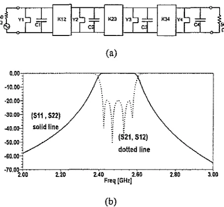
The Figure l(a) shows combline bandpass filter circuit
and its components which are operating in a 50
n
system.The element values of equivalent combline bandpass
filter in a 50
n
system are shown in Table I. Thesimulated response of combline bandpass filter is shown
in Figure I (b ). It has design specification as follows:
Center frequency of2.5 GHz with 160 MHz bandwidth. The insertion loss of 0.1 dB insertion loss and return loss better than 20 dB is achieved especially in the passband.
(a)
o.oo-J MMMMᄋMMセN@
セqooセ@ :
j : .
:3
QZセZQ@
iyy\
..so:oo4
j
HセRQL@
512)1 dotted line
·60,00-:j 1
ᄋWPNdセセo@ 2.20 2.40 a.so 2.80 3.00 Freq [GHz]
(b)
[image:3.595.304.525.104.375.2]Figure I: (a) Comblinc filter operate in a 50 n system, (b) Frequency response of bandpass filter.
Table l: Element values for comb line bandpass filter Element of
eombline
Values bandpass
Filter
C1=C., 15.9894 pF
Ci= C3 38.1670 oF
Y1=Y., 9.1327 mho
Y2=Y1 22.0488 mho K,?= K34 1.3193
K23 1.5751
The equivalent circuit of the combline band filter can now be transformed to physical layout as shown in Figure 2. Figure 3 shows the dimension of physical filter.
QMNLᄋセイᄋf@
I
I
I
Figure 2: Physical filter layout
b
Side •·ici•·
Topl"iew
FJ"Ont 1·iew
Figure 3: Dimensions of physical filter (a) top view, (b) side view
The dimensions of the physical filter can be determined using the following formulas:
Cavity diameter, b, in mm:
I..
<
b<
0.2 I.. (7)where
ii.
is the wavelength at 2.5 GHz.Resonator diameter, d, in mm:
0.2b
<
d<
0.4b (8}Rod diameter is a function of its impedance and cavity diameter. Hunter [2] gives the characteristic impedance,
z.,
ofround rod between two ground planes as:z.
=
138x
log[;:J
(9)The distance between the end wall and first or last
resonator, e, can be found using:
[image:3.595.52.279.319.529.2] [image:3.595.89.241.585.722.2]s-1memauonai Lonrerence on t.ngmeermg ano IC I ttCt.ILU IL) Melaka, Malaysia
4-6 April 2012
M
=
o.69sd2gap 100C-2.61d (l l)
where C is the loading capacitance, and dis rod diameter.
The distance between resonators, Scomb(i.i)• can be
calculated using:
Scomb(i,j)
=
QNセ
W@
[ ( 0.91セI@
+
0.048 - log(;· /(8) · K i.j)J
(12)where
and
f(B)
=
セイQ@
2Kセ}@
smze8 = Rョセ@
A.
(13)
(14)
The physical layout parameters are listed in Table 2.
Table I: dimensions of real layout filter
Physical layout parameters
· Cavitydian1eter (h)
Resonator diameter (d)
Reson11i<lr Jengtll (/) Tap point distance from the
ground Minimum gap (Mgap) Center to center spacing between
resonators (SiJ) Distance between end wall to
center of end rod (e)
Values (mm)
8
. 12
3.5
0.5
19.5, 21.5, 19.5
14
[image:4.595.313.529.88.200.2]The physical layout filter is modeled and simulated using 3D Ansoft HFSS software as shown in Figure 4.
Figure 4: 30 HFSS Model of physical filter
The response of filter simulation by HFSS software is shown in the Figure 5. The insertion loss of about 0.1 dB
insertion loss and return loss better than 13 dB is achieved especially in the passband.
0.0 •
ᄋQPNPセ@ 4
-20.00-; J
-30.00-3
MQPNPPセ@
MUPNPPセ@
セ@
.ii0.001
MWPLPPセ@
(S11, 522)
solid line (521, 512) dotted line
MウッNッセᄋKMQPMMMRNセRPMMMRセNTMP@
_ _ _RNgセッMMMRNセXッMMMMMMャSNッッ@
[image:4.595.47.253.347.509.2] [image:4.595.322.515.437.731.2]Freq [GHz}
Figure 5 response of real physical filter simulation as 30
The filter requires further tuning and optimization in order to obtain good response [6]. However, due to the structure of this non-planar filter, it requires a powerful and high performance of computer to perform the optimization.
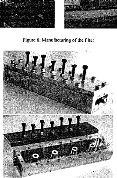
V. FABRICATION AND MEASUREMENT The filter was manufactured in workshop at the Faculty of Manufacturing Engineering (FKP), Universiti of Teknikal Malaysia Melaka, (UTeM) using CNC machine and aluminum as its material (Figure 6). The photograph of the filter is shown in Figure 7.
Figure 6: Manufacturing of the tilter
[image:4.595.73.282.556.703.2].,.- 1mcmauona11.,omcrcnce on tngmeermg ana 11., 1 \l\.,t!L.U IL.)
Melaka, Malaysia 4-6 April 2012
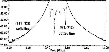
The filter was tested and measured using Vector Network Analyzer. The measured response is shown in Figure 8. Table 3 shows the comparison between the simulated and measured results. An excellent agreement between the EM simulations and measurement has been achieved especially in the passband.
O.OIJ-'.::-· MMMMMMM]M[]セ]]MZLNLNMMMMMM]]ゥ@
ᄋQPNPPセ@
•
·20.00-j
セ@
-30.00-:]
.,
MTdNooセ@ j
-50.001
'
[S11, S22)
(521, 512)
dotted line
MWPNPPQMKセMMMセMMMMMMMセMMセMMMMゥ@
2.00 2.20 2.40 2.60 2.BO 3.00
Freq [GHz]
[image:5.595.57.279.152.259.2]Figure 8: Measured response of physical filter
Table 3: Comparison between EM Simulations and Measurement
Equivalent Simulation Measurement distributed 3D
circuit
Center Freq. 2.5 2.48 2.5
GHz
Pass-band B.W 160 170 173
[MHz]
sエッーセ「。ョ、@ B. W ·. 320 300 290
.· [MHz)···
SI I [dB] -20 -12 -15
Sl2 [dB) -0,04 -0.35 cQ.87
S21 [dB] ·0.04 -0.34 -0.85
S22[dBj -15 -15 ·15
VI. CONCLUSION
This paper has demonstrated a systematic development and design of combline filter based on coaxial resonators technology. This class of microwave filter would be useful in any transceiver systems where the low-loss and high selectivity performance are required. The main advantage of coaxial resonator filter has been with its
post-manufacturing tuning capabilities and good
selectivity. Thus, the filter could easily be tuned and optimized in the laboratory in order to obtain the desired response. In addition, a diplexer or multiplexer is recommended be designed for practical applications such as in radio base station and satellite transponder.
ACKNOWLEDGMENT
Z. Zakaria would like to thank UTeM for sponsoring this
work under the short term grant, UTeM,
PJP/2011/FKEKK (4C)/S00838.
REFERENCES
[I] I. C. Hunter, R. Ranson, A. C. Guyette, and A. Abunjailch, "Microwave filter design from a systems perspective", IEEE Microwave Magazine, October 2007.
[2] I. C. Hunter, Theory and Design of Microwave Filters. Stevenage, UK: IEE, 2001.
[3] G. Matthaei, L. Young, and E.M.T. Jones, Microwave Filters, Impedance Matching Networks and Coupling Structures.Dedham,
MA: Artech House, 1964.
[4] M. J. L. Jia-Shen G. Hong, Microstrip Filters For RF/ Microwave Applications. Canada: John Wiley & Sons, Inc., 2001.
[5] D. M. Pozar, Microwave Engineering. Hoboken, NJ: John Wiley &
Sons, Inc., 2005.
[image:5.595.58.275.321.489.2]