DESIGN AND ANALYSIS OF LOW NOISE AMPLIFIER
USING CADENCE
M. I. IDRIS1, N. YUSOP 2, S. A. M. CHACHULI3,M.M. ISMAIL 4 FAIZ ARITH 5 AND N. SHAFIE6
1,2,3,4,6
Faculty Of Electronics & Computer Engineering, Universiti Teknikal Malaysia Melaka, Hang Tuah Jaya, 76100 Durian Tunggal, Melaka, Malaysia
E-mail: 1
4
[email protected] , [email protected] , [email protected]
ABSTRACT
Low Noise Amplifier also known as LNA is one of the most significant component for application in wireless communication system. It is a very important part in RF receiver because it can reduce noise of gain by the amplifier when the noise of the amplifier is received directly. The low noise amplifier has been designed to get the better performance by follow the requirement in this new era consists of high gain, low noise figure, lower power consumption, small chip area, low cost and good input and output matching. In this research, a LNA schematic consists of three stages which are common gate amplifier, common drain amplifier and active inductor is designed to mitigate this constraint. Common gate and common drain are used for input and output stages in every LNA. Both are also used for excellent input and output matching and have a potential to get a lower noise whereas for active inductor, it is used to obtain the lower power consumption and to reduce the chip size in layout design. The results show that the proposed LNA is able to achieve the best performance with a simulated gain of 14.7dB, extremely lower power consumption of 0.8mW, noise figure of 7dB and small chip area 0.26mm². Consequently, this modified LNA is appropriate for low-voltage applications especially in wireless communication system.
Keywords: Low Noise Amplifier, inductor, cadence, RF receiver and high gain.
1. INTRODUCTION
Low noise amplifier also known as LNA is a special type of electronic that widely used in wireless communication system. A LNA can be found in RF transmitter and receiver for the basic building block in communication system. Hereby, LNA is a very important part of the receiver because it is placed at the front of the receiver and act as an amplifier to amplify the received signals as an electronic amplifier in order to get the level that required with the minimum produced their own additional noise. Basically, radio receiver consists of amplifier, mixer and filter.
Furthermore, the main function of LNA is to amplify a very low signal. This amplification is without adding noise to maintain the required signal to noise ratio at very low power level and for higher
signal levels and also the receiver which is receiver sensitivity can be received when the amplification provides the first level. By using this design, the noise can be reduced by the gain and also by the amplifier while the noise of the amplifier is inoculated directly into the received signal.
Figure 1 Block Diagram Of RF Transceiver[1]
2. LNA TOPOLOGIES
Low noise amplifier is the first stage in and it is very important part in RF receivers. Hereby, low noise amplifier should be matched with the antenna characteristic. The characteristics of antenna are excellent input and output matching and high gain.
To optimize the low noise amplifier design, the suitable topology should be selected for low power and low voltage. For shunt series feedback common source topology, it is difficult to trade of among gain, small noise figure and good input and output matching with very low power consumption. Meanwhile, for common gate topology, the gain less than 10dB with very low power consumption.
Next, the noise must add to the LNA because of the resistor thermal noise for resistor termination common source topology. Besides that, the specification is satisfied for inductive degeneration common source topology in very low power consumption but the isolation is not good enough compared to the cascade inductor source degeneration topology which can get the similar low noise amplifier performance with very low power consumption. Lastly, for cascade inductor source degeneration topology provides higher gain with a low noise figure.[2]
Hence, there are several fundamental types of topologies for low noise amplifier and a common low noise amplifier has been choosen for optimizing the LNA design. Figure 2 shows the toplogies of LNA:
Figure 2 Fundamental Of Topologies LNA:(A)Shunt Series Feedback Common Source (B)Inductive
Degeneration Common Source (C)Common Gate (D)
Resistive Termination Common Source (E)Cascode Inductor Source Degeneration[2]
3. METHODOLOGY
In this design there are mainly three stages in the proposed LNA. Every stage is explained in greater detail in Figure 3.
Figure 3 Block Diaram Of Three Stages LNA[3]
1. Common Gate Amplifier
Basically, common gate amplifier is widely used in electronic field and one of three basic single stages field-effect transistor (FET) topologies. The advantages by using this FET are:
i. Used as current buffer or voltage amplifier.
ii. Used as input stage for LNA iii. Obtain input impedance matching.
The input impedance depends only on the trans-conductance of CMOS shown in equation 1.
1 gm
2. Active Inductor
The active inductor has been implemented in this design which performs the same function as passive inductors. Active inductor is a combination of CMOS transistors. To design a low noise amplifier it has a fewer difficulty but it has higher flexibility to get the input and output matching, easy to design the layout and it does not have the magnetic field. For this design it does not used the real active inductor as main function but change it with transistor that perform the same function with active inductor. The advantages by using active inductor are:
i. To get lower power consumption. ii. Used to reduce chip area iii. Used to reduce complexity iv. Used to reduce cost
v. Used to compensate for the affect of parasitic capacitors at high frequencies
(a) (b)
Figure 4 Active Inductor Circuit And His Equivalent Circuit[3]
In figure 4(a) and (b), the quality factor (Q) inductance (L), and frequency (w) is calculated from the equation below:[3]
gm4gm3Cgs3 1 Rfgds4gds4ଶCgs4
This quality factor is high enough because it depends on Rf.
Cgs31 Rfgds4gm4gm3
Cgs4Cgs31 Rfgds4gm4gm3
After the design is implemented with the equivalent circuit, it has been improved by using double feedback with second order. Figure 5 shows the active inductor after the improvement.
Figure 5 Double Feedback With Second Order Circuits[3]
3. Common drain amplifier
Common drain amplifier is one of three basic single-stages (FET) amplifier topologies also known as a source follower. It is usually used as a voltage buffer. The advantages by using this FET are:
i. Used as a final stage in every LNA ii. Capable to get small output
impedance matching iii. Potentially has lower noise
4. LITERATURE REVIEW
Table 1 Comparison Of The LNA Design
(We are unable to place the figure here due to its size which is
placed at the endof the manuscript)
4.1 Proposed A Low Noise Amplifier Circuit
From the comparison the proposed a low noise amplifier circuit has been selected based on the best performance in term of the noise figure, high gain and power consumption. The proposed low noise amplifier circuit uses the active inductor to achieve the requirements. In addition, it is implemented with latest CMOS technology 0.13µm.
(We are unable to place the figure here due to its size which is placed at the below of the manuscript)
Figure 6 Schematic Of Proposed Low Noise Amplifier[3]
4.2 Enhancement Circuit
This circuit will be modified from the researcher Hamzeh Fatehi. This design will enhance with the change of CMOS technology from 0.18µm to 0.13µm. Furthermore, the transistor size also will be change.
Table 2 Transistor Width [3]
4.3 Design Specification Of LNA
There are some important specifications that LNA should achieve. The specifications of LNA design are indicated in Table 3
Table 3 Specifications Of LNA Design[6]
5. DISCUSSION AND RESULTS
Design and analysis of low noise amplifier is designed and simulated by using CADENCE software with latest technology 0.13µm. The DC biasing voltage values for this design are V1= 1.1, V2=0.6, V3=0.6 and Vgg=0.7 respectively.
In this new design the ratios (W/L) of the transistor that used in this circuit have been fixed. For the transistor lengths the value are 0.13µm for all transistors while the transistor width the value are different by using the manual calculation. Figure 7 shows the schematic circuit of the proposed LNA design and Table 4 shows the transistor ratio after the enhancement.
Figure 7 Schematic Of Proposed Low Noise Amplifier After Enhancement
5.1 Major Challenging
While completing the design, there are major challenges arise of producing the right value of gain. On the first experiment, all the transistors are combined into one ground nodes. The result shows that, gain value is negative. So, it does not meet the requirement of gain which it must be in positive value. Then it proceeds to second experiment. The ground nodes are connected to each transistor respectively. Based on these experiments, it can be concluded that the ground nodes cannot be combined because of the input DC biasing value for each transistor is different. Figure 8 and 9 show the gain in negative value and positive value.
Figure 8 Gain In Negative Value
Figure 9 Gain In Positive Value
The best design for low noise amplifier is capable to achieve the highest value of gain and it have to be more than 10dB based on the specification of LNA design [6]. An adjustment has been made to the value of DC bias. After few trials the highest gain is successful achieved is 14.7dB. In order to get this value, the Vgg decrease to 0.5 V while V1 is increased to 1.2 and the rest are remaining. The transistor width for M4 also changes to the 0.5µm. Table 5 shows the analysis that have been made to get gain in positive value.
Table 5 Analysis Of Gain Value
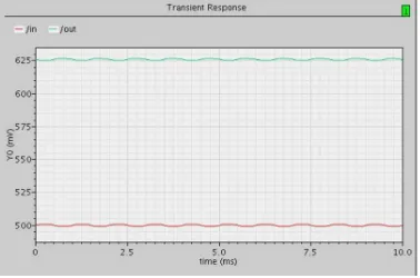
5.2 Transient Analysis
must greater than the input signal. Figure 10 shows the simulation result of transient analysis
.
Figure 10 Transient Analysis Simulation
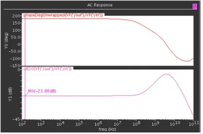
5.3 AC Analysis Result
After transient analysis is done, the AC analysis for LNA design is obtained. To achieve the desired specifications gain, optimum transistor width, input value of DC biasing voltage was the main criteria for design of LNA[15,16]. When high gain has been achieved the noise can be reduce by gain of the amplifier that captured by antenna. To obtain the gain of the LNA design, below expression can be used[17]:
20log₁₀VoutVin
For this design the gain is successfully achieved with 14.7dB based on the design specification. Figure 11 shows the simulation result of gain in AC analysis
Figure 11 AC Analysis Simulation
5.4 Summary Of Simulation Result
The overall of the specification of LNA design were met. The simulation results are shown in the Table 6 below:
Table 6 Simulation Result
5.5 Layout Design
In figure 12, the layout of low noise amplifier is designed by using CADENCE software with 0.13µm CMOS technology. The parameters of transistor width are followed as in Table 4. It also shows the smallest chip area which is 0.26mm².
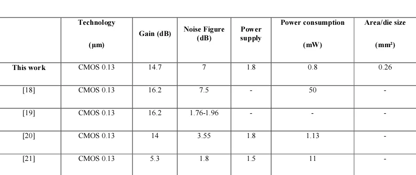
5.6 Comparison With Other Published Work
Table 7 shows the summary of proposed LNA design simulation result and comparison with other published work.
(We are unable to place the figure here due to its size which is placed at the below of the manuscript)
Table 7 Comparison With Other Works
6. CONCLUSION
An improved design of low noise amplifier using active inductor is presented in this research. The modified circuit has bee design by using the CADENCE 0.13um CMOS technology. The objective of this design was accomplished based on the specifications of the LNA. According to the resesearch result, the circuit is capable to achieve gain of 14.7dB, noise of 7dB, extremely low power consumption of 0.8mW, good input and output matching. However it has the problem with the noise due to the usage of the latest technology which is 0.13µm. it is designed by using CADENCE software with latest technology 0.13µm. Lastly, the circuit size reduced significantly to small chip size of 0.26mm².
ACKNOWLEDGEMENTS
The authors would like to thank to University Teknikal Malaysia Melaka (UTeM) and Ministry of Higher Education for the support, facilities and financial support throughout the project.
REFERENCES:
[1] J. Brown, “Design of a Magnetically Tunable Low Noise Amplifier in 0 . 13 um CMOS, "(2012). Graduate Thesis and Dissertations, Paper 12672.
[2] S. Kumar, “CMOS Low Noise RF Amplifier Design and Parameter Estimation using ANN ,”Master of Technology in VLSI Design &CAD vol. 147004, 2012.
[3] H. Aljarajreh, M. B. I. Reaz, M. S. Amin, and H. Husain, “An Active Inductor Based Low Noise Amplifier for RF Receive," Department of Electrical, Electronic and
Systems Engineering, UKM, ISSN 1392-1215,Vol.19, NO.5,2013.
[4] N. Moser, S. J. Rogers, P. Supervisor, and J. Rogers, “ELEC 4907 – Fourth Year Engineering Project Final Report A 5 . 2 GHz Differential Cascode Low Noise Amplifier,” 2004.
[5] P. Version, “Low Noise Amplifier Design Measuremants,” Inc.,555 Riber Oaksparkway, San Jose, CA 9514, USA,, Product Version 5.0, September 2004.
[6] N.Rani, S.Sharma, “Design of Low Noise Amplifier at 3-10GHz for Ultra Wideband Receiver,”international Journal of Innovation Research in Computer and Communication Engineering, Vol.1, Issue 7, September 2013.
[7] P. Kavyashree and S. S. Yellampalli, “The Design of Low Noise Amplifiers in Nanometer Technology for WiMAX Applications,” M.Tech(VLSI Design), VTU Extension Centre, UTL Technologies Limited Bangalore, India,vol. 3, no. 10, pp. 1–6, 2013.
[8] P. G. Afshar, “International Journal of Advanced Research in A 3 . 5 GHz Low Noise Figure Mixer with High Conversion Gain for WiMAX Systems,” IEEE of Advanced Research in Compuetr Science and Software Engineering, vol. 3, no. 5, pp. 695–699, 2013.
[9] B. Liu, C. Wang, M. Ma, and S. Guo, “An Ultra-Low-Voltage and Ultra-Low-Power,” School of Computer and Communication, Hunan University, China vol. 18, no. 4, pp. 527–531, 2009.
[10] A. Goel and G. Singh, “A Novel Low Noise High Gain CMOS Instrumentation Amplifier for Biomedical Applications,” Centre for Development of Advanced Computing (C-DAC), Mohal, India, vol. 3, no. 4, pp. 516–523, 2013.
a Cable Tuner.,” Final project Report., vol. 51, no. 2, p. Contents2, Jan. 2014.
[12] E. D. Link, “CMOS LNA Design for Multi-Standard Aplication,” Master Thesis at Electronic Devices Linkopings Institute of Technology, 2006.
[13] S.-S. Kim, Y.-S. Lee, and T.-Y. Yun, “High-Gain Wideband CMOS Low Noise Amplifier with Two-Stage Cascode and Simplified Chebyshev Filter,” ETRI J., vol. 29, no. 5, pp. 670–672, Oct. 2007.
[14] R. R. Harrison, C. Charles, and S. Member, “A Low-Power Low-Noise CMOS Amplifier for Neural Recording Applications,” IEEE Journal of Solid-State Circuits vol. 38, no. 6, pp. 958–965, June 2003.
[15] M. Idzdihar Idris, M.N. Shah Zainuddin, M. Muzafar Ismail, R. Abd. Rahim, “Design of a Low Voltage Class AB Variable Gain Amplifier (VGA)”, Journal of Telecomunication, Electronic and Computer Engineering(JTEC),Vol.4 No.2, ISSN:2180-1843 , pp . 69-74, 2012.
[16] Idris, M. I. B., Reaz, M. B. I., Bhuiyan, M. A. S., A Low Voltage VGA For RFID Technology”, Receivers, 2013 IEEE International Conference on RFID-Technologies and Applications, (2013), 1-4
[17] Mohammad Arif Sobhan BHUIYAN, Muhammad Idzdihar Bin IDRIS, Mamun Bin Ibne REAZ, Khairun Nisa MINHAD, Hafizah HUSAIN “Low Voltage and Wide Bandwidth Class AB Variable Gain Amplifier in 0.18-μm CMOS Technology”,
PRZEGLĄD ELEKTROTECHNICZNY,
ISSN 0033-2097, R. 90 NR 6/2014 , 184-187.
[18] J. Brown, “Design of a Magnetically Tunable Low Noise Amplifier in 0 . 13 um CMOS Technology,” 2012.
[19] P. Jha and P. Vishwakarma, “Design of RF Front-End Low Noise Amplifier for an Ultra Wideband Receiver,” Electronics &Communication Department,NIET Greater Noida, India,Journal of Electron Devices, Vol. 13, pp. 1006–1011, 2012.
[20] T. Thi and T. Nga, “Ultra power low-noise amplifier designs for 2 . 4 GHz ISM band applications,” School of Electrical & Electronic Engineering no. July, 2012.
Table 1 Comparison Of The Lna Design
Technology Gain (dB) Frequency (GHz) Noise Figure (dB)
Power supply
Power consumption
Area/die size
[3] CMOS 0.18 20 2-3 3.1 1.8 0.5 0.003
[5] CMOS 0.18 15.04 8.72 3.85 1.8 4.7 -
[6] CMOS 0.18 17.04 5.8 3.1 1.8 6.4 -
[7]
CMOS 0.18 15.7
19.9
5.9
5.9
1.85
2.63
1
1
19.3
56.8
-
-
[8] CMOS 0.18 1.2 3.5 6.5 1.5 10.12 -
[9] CMOS 0.18 14.3 2.4 1.6 1.8 0.9 -
[10] CMOS 0.18 67.7 - - - - -
[4] CMOS 0.18 19.5 5.2 2.7 3 - -
[11] CMOS 0.18 12-14 - - 5.5-6 - -
[12] CMOS 0.18 - 2.4 2.17 - - -
[13] CMOS 0.18 - 8.2 3.3-6.3 - 17.3 -
[14] - 39.8 - - 2.5 - 0.2
Table 7 Comparison With Other Works
Technology
(µm)
Gain (dB) Noise Figure (dB)
Power supply
Power consumption
(mW)
Area/die size
(mm²)
This work CMOS 0.13 14.7 7 1.8 0.8 0.26
[18] CMOS 0.13 16.2 7.5 - 50 -
[19] CMOS 0.13 16.2 1.76-1.96 - - -
[20] CMOS 0.13 14 3.55 1.8 1.13 -
![Figure 3 Block Diaram Of Three Stages LNA[3]](https://thumb-ap.123doks.com/thumbv2/123dok/514798.58675/2.595.306.520.447.492/figure-block-diaram-stages-lna.webp)
![Figure 5 Double Feedback With Second Order Circuits[3]](https://thumb-ap.123doks.com/thumbv2/123dok/514798.58675/3.595.87.282.396.561/figure-double-feedback-second-order-circuits.webp)
![Table 2 Transistor Width [3]](https://thumb-ap.123doks.com/thumbv2/123dok/514798.58675/4.595.305.500.487.654/table-transistor-width.webp)