i
HIGH LINEARITY POWER AMPLIFIER FOR WCDMA APPLICATION
SITI NUR LIYANA BT ISMAIL
This Report Is Submitted In Partial Fullfillment Of Requirement For The
Bachelor Of Electronic Engineering (Telecommunication Electronics) with
Honours
Faculty Of Electronic And Computer Engineering
Universiti Teknikal Malaysia Melaka
ii ii ii ii ii
ii
ii
iii ii ii ii ii ii ii ii ii ii
ii
v
vi
ACKNOWLEDGEMENT
My gracious thanks to Allah for giving me strength to complete my final year project successfully. I would like to convey my greatest gratitude and appreciation to my supervisor Pn. Siti Fatimah Bt. Sulaiman for her invaluable help, support and guides thoroughout my project and also to my co-supervisor En. Harris B. Misran. Her brilliant ideas, suggestion and expertise in this field are sincerely and highly appreciated.
vii
ABSTRACT
viii
ABSTRAK
ix
Table of contents
CHAPTER TITLE PAGE
ACKNOWLEDGMENT
vi
ABSTRACT vii
ABSTRAK viii
TABLE OF CONTENTS ix
LIST OF TABLES xii
LIST OF FIGURES xiii
LIST OF ABBREVIATIONS xiv
LIST OF APPENDICES xv
I INTRODUCTION
1.1 Project Background 1
1.2 Problem Statement 1
1.3 Objective 2
1.4 Scope of Work 2
1.5 Thesis Outline 3
II LITERATURE REVIEW
2.1 Introduction 4
2.2 History of WCDMA 4
2.3 Characteristic of Power Amplifier 5
2.3.1 Linearity 5
2.3.2 1 dB Compression point (P1dB) 6
2.3.3 Intermodulation Distortion 7
2.3.4 Third Order Intercept Point 8
2.3.5 Efficiency 9
2.3.6 Adjacent Channel Power Ratio 10
2.3.7 Effect of Nonlinearity on a W-CDMA System 11
2.4 Classe of Amplifier 11
2.4.1 Class A, AB, B, and C Power Amplifiers 12
2.4.2 Class A 13
2.4.3 Class B 15
2.4.4 Class AB 16
2.4.5 Class C 16
x
2.4.7 Class E 18
2.4.8 Class F 20
2.5 TopologyOf Power Amplifier 20
2.5.1 Reactive Matching 21
2.5.2 Balanced Amplifier 21
2.5.3 Feedback Amplifier 22
III METHODOLOGY
3.1 Introduction 25
3.2 Methodology 25
3.2.1 Flow Chart 27
3.3 Design Specification 30
3.4 Transistor Selection 30
3.5 Stability 30
3.6 Biasing 31
3.7 Matching Network 32
3.8 Simulation of power Amplifier 35
3.9 Optimization and Analysis 35
IV RESULT AND ANALYSIS
4.1 Design of Power Amplifier 36
4.1.1 Bias Point Simulation 36
4.1.2 Measurement Transistor 38
4.1.2.1 Scattering Parameter and Stability 38
4.1.3 Two Port Power Gain 40
4.1.4 Maximum Conjugate 41
4.1.5 Matching Network 42
4.1.6 Microstrip Implementation 43
4.1.7 DC Biasing 44
4.1.8.Implementation of Power Amplifier 45
4.1.9 Analysis Result of Single Stage Power Amplifier 45 4.1.10 Output Power Analysis for Single Stage Amplifier 46
4.2 Design of Balanced Amplifier 48
4.2.1 Result Analysis of Balanced Amplifier 48 4.2.2 Output Power Analysis for Balanced Amplifier 49
4.3 Design of Feedback Amplifier 50
4.3.1 Result Analysis of Feedback Amplifier 50
4.3.2 Output Power Analysis for Feedback Amplifier 51
4.4 Analysis Summary 52
V CONCLUSION
5.1 Conclusion 55
5.2 Future Work 56
xi
LIST OF TABLES
NO TITLE PAGE
1 Adjacent channel power for 3G standard 11
2 Design specification for High Linearity Power Amplifier 30
3 Specification for FR-4 material 34
4 Comparison of stability between calculation and simulation 39
5 Comparison of gain 41
6 Result of input and output matching 42
7 Analysis of Single Stage Amplifier 53
8 Analysis of Balanced Amplifier 53
9 Analysis of Feedback Amplifier 54
xii
LIST OF FIGURES
NO TITLE PAGE
1 Evolution of wireless network system 6
2 1dB compression point 7
3 IMD3 in a nonlinear system 8
4 Third Order Intercept Point 9
5 Adjacent Channel Power Ratio 10
6 General schematic for power amplifier 12
7 Waveform of class A 13
8 Conduction angle for classical 15
9 Waveform of class B 16
10 Waveform of class C 17
11 Class D amplifier 18
12 Class E Amplifier 19
13 Voltage and Current waveform for class E 19
14 Example of class F amplifier 20
15 Balanced Amplifier Configuration 22
16 General negative feedback system 23
17 Passive biasing 31
18 a) and b) high pass version c)and d) low pass version 33
19 FET curve tracer 37
20 Transistor IV vurve 37
21 Stability schematic design 38
xiii
23 Schematic for input and output matching 44
24 Schematic for DC biasing 44
25 Complete Single Stage Power Amplifier 45
26 Result for S-Parameter 46
27 Harmonic Balance Schematic diagram 47
28 Output power for Single Stage 47
29 Schematic of Balanced Amplifier 48
30 S-Parameter for Balanced Amplifier 48
31 Simulation for Output Power 49
32 Result for Output Power 50
33 Feedback Amplifier design 50
34 Simulation result of S-parameter for Feedback Amplifier 51
35 Schematic for Output Power Analysis 51
xiv
LIST OF ABBREVIATION
ADS ADVANCED DESIGNED SYSTEM
ACPR ADJACENT CHANNEL POWER RATIO
E-PHEMT ENHANCEMENT MODE PSEUDOMORPHIC HEMT
HEMT HIGH ELECTRON MOBILITY TRANSISTOR
FET FIELD-EFFECT TRANSISTOR
DC DIRECT CURRENT
FDD FREQUENCY DIVISION DUPLEX
GSM GLOBAL SYSTEM FOR MOBILE
IMD3 THIRD ORDER INTERMODULATION DISTORTION
IP3 THIRD ORDER INTERCEPT POINT
PA POWER AMPLIFIER
PAE POWER AMPLIFIER EFFICIENCY
PHS PERSONAL HANDPHONE SYSTEM
P1dB 1DB COMPRESSION POINT
QPSK QUARTER PHASE SHIFT KEYING
RF RADIO FREQUENCY
TDD TIME DIVISION DUPLEX
WCDMA WIDE-BAND CODE DIVISION MULTIPLE ACESS
xv
LIST OF APPENDICES
NO TITLE
1
CHAPTER 1
INTRODUCTION
1.1Project Background
Mobile communication has become quite common in today’s world with the
increasing needs of effectively utilized bandwidth, and efficient and compact device technologies. The growth of wireless technologies is expressly fast. The information can easily communicate by the mobile communication system such as GSM, PHS, and third generation Wide-Band Code Multiple Access (W-CDMA). The wireless networking systems such as wireless local area network (WLAN), Bluetooth also are developed. High speed and high data rate are always required to provide better communication qualities and services in these wireless systems.
Power amplifiers (PAs) are typically blocks of RF front end circuits, which take more care to get efficient RF PA for saving the power consumption. However, Pas has most efficient when operating at compressed region as a nonlinear amplifier [1].
2
design the high efficiency amplifier with the non-linear mode combined with a complex linearity improvement technique such as Doherty amplifier, DC-DC converter amplifier
1.2 Objective Of Project
The objectives of this project is to study the characteristic and specification of high linearity power amplifier for wireless communication which is for WCDMA application. Besides, design a high linearity power amplifier that can be used for WCDMA application and simulate by using Agilent Advanced Digital Software (ADS).
1.3 Problem Statement
High efficiency and good linearity are among the important characteristics of a base station that power amplifier used in plurality of the communication applications. Both the characteristics have always been contradictory to demand for creative power amplifier design techniques. Maintaining the high efficiency which over a wide range of the power amplifier operation is an added requirement in these applications making power amplifier design a challenging task.
1.4 Scope of project
Scope of this project can be divided into three parts which are: a) Literature review
Ø The study of RF fundamental and characteristic of the high linearity power amplifier especially on the gain, return loss, stability which must be taken into consideration in designing this project.
b) Design and simulation
3
c) Test analysis and measurement
Ø The performance of the designed amplifier will be tested and compared with the simulation result.
1.5 Thesis Outline
This thesis is a document that delivers the ideas generated and the concepts applied in this project. In chapter one contains the introduction of high linearity power amplifier for WCDMA application. The introduction consists of project background, objectives, problems statement, scope and thesis outline.
Meanwhile, chapter two is the project literature review. In order to execute this project, literature review must be done to comprehend the whole system and to decide the best inputs, outputs and used devices. Data obtained from the journal, books, magazines and internet.
Chapter three describes the methodology of the project flow and its functional block diagram. It also discusses the method used for the project, such the software applied.
Chapter four consist of actual result and analysis of this project. It included all the main components together with the functionality and description applied in this project.
4
CHAPTER II
LITERATURE REVIEW
2.1 Introduction
In order to execute this project, literature review must be done to comprehend the whole system and to decide the best inputs, outputs and used devices. From literature review, there will be an analysis regarding the method are used for complete this project. Literature review also will help to gain more information about the high linearity power amplifier for WCDMA application.
2.2 History of WCDMA
5
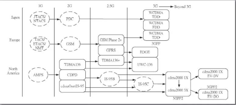
[image:20.612.137.525.168.342.2]frequency. At modulation technique, QPSK has been introduced for W-CDMA system which higher data rate and global roaming around the multi-standard communication sets, to achieve linear 3 capabilities is being important issues of mobile handset. The system will provide a high data services up to 3.84Mbps.
Figure 1 :Evolution of wireless network system
2.3 Characteristics of Power Amplifier
2.3.1 Linearity
6
· 1dB compression point (P1dB)
· Third order intermodulation distortion (IMD3) · Third order intercept point (IP3)
· Efficiency (PAE)
· Adjacent channel power ratio (ACPR)
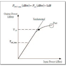
2.3.2 1dB compression point (P1dB)
7
Figure 2: 1dB compression point
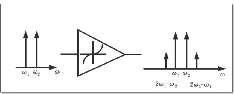
2.3.3 Third order intermodulation distortion (IMD3)
8
Figure 3 : IMD3 in a nonlinear system
2.3.4 Third Order Intercept Point (IP3)
9
Figure 4 : Third Order Intercept Point
2.3.5 Efficiency
Efficiency in power amplifiers is expressed as the part of the dc power that is converted to RF power, and there are three definitions of efficiency that are commonly used. Collector efficiency is the ratio of the RF output power to the dc input power.
ߟ ൌೀೆ ವ
Power-added efficiency (PAE) describes the power of the input signal into account and can be expressed by
ܲܣܧ ൌೀೆିಿವ ൌಿൈሺீିଵሻವ
PAE is generally used for analyzing PA performance when the gain is high. Finally, the average power efficiency is a measure of the ratio of the total energy transmitted to the total energy drawn usable for all kinds of performance evaluations.
(2.1)