v
ACKNOWLEDGEMENT
First, I would like to thank Mr. Radi Husin Bin Ramlee who was giving me a chance to be a final year project student of him; guiding me within the whole flow of my final year project; and sharing knowledge those are very useful for helping me to solve the problems faced within period of doing the project. The experiences and knowledge gained will also be a very useful references and tools in my future studies or work. I really appreciate all the things that I had learnt in this whole year on my final year project, the writing skills practiced on writing thesis of project and experiences gained by doing lots of surveys and problem solving with other Verilog HDL teammates.
vi
ABSTRACT
vii
ABSTRAK
viii
2.1 Field-Programmable Gate Arrays (FPGAs) 6 2.1.1 FPGAs vs. Programmable
Logic Devices (PLDs) 7
2.1.2 FPGAs vs. Application-Specific
ix
2.2 Altera DE2-115 Development and Education
Board 8
2.3 Video Graphics Array (VGA) Controller 10
2.3.1 VGA Specifications 10
2.3.2 Pixel on Screen 12
2.3.3 Five Control Signal 13
2.3.4 Sync Timing 14
2.3.5 Counting Clock Cycle 15
2.4 Verilog Hardware Description Language 17 2.4.1 Capabilities of Verilog HDL 18 2.5 Altera Quartus II Compiler Software 18
2.5.1 Quartus II Web Edition 19
2.5.2 Quartus II Subscription Edition 20
III METHODOLOGY 21
3.1 Project Planning 21
3.2 Literature Review 22
3.3 Study the Programming Language 22
x
Quartus II Compiler Software 39 4.2.4.2 Pin Planner in Altera Quartus II
Compiler Software 41
4.2.4.3 Register Transfer Level (RTL)
Viewer 43
4.2.4.4 VGA Controller on Altera DE2-115 Development and Education Board 45 4.2.5 VGA Controller Verilog HDL Coding 46
V CONCLUSION AND SUGGESTIONS 54
5.1 Project Limitation 54
5.2 Future Works 54
5.3 Conclusion 55
VI REFERENCES 56
xi
LIST OF FIGURE
NO TITLE PAGE
1.2.1 The use of paper as poster at cinema and menu at restaurant 3 2.2.1 Altera DE2-115 Development and Education Board 8 2.3.1.1 Female port and male port on VGA Connector 11
2.3.2.1 Scanning pattern of VGA Controller 13
2.3.4.1 The horizontal and vertical synchronization
signal-timing diagram 15
2.5.1 Interface of Quartus II 11.1sp2 Web Edition (32-Bit) 19 3.7.1 Flow Chart diagram of the design and implementation of
VGA Controller on FPGA (i) 24
3.7.2 Flow Chart diagram of the design and implementation of
VGA Controller on FPGA (ii) 25
4.1.1 Conversion of VGA picture in bmp format to MIF file 27
4.1.2 Expected result 27
4.2.1.1 Block diagram of VGA controller 28
4.2.2.1.1 Flow chart for vga_sync module (i) 30
xii
4.2.2.1.3 Flow chart for vga_sync module (iii) 32
4.2.2.1.4 Flow chart for vga_sync module (iv) 33
4.2.2.1.5 Flow chart for vga_sync module (v) 34
4.2.2.1.6 Flow chart for vga_sync module (vi) 35
4.2.2.2.1 Flow chart for vga_controller module 36
4.2.3.1.1 Waveform obtained from vga_sync module 37 4.2.3.1.2 Waveform obtained from vga_sync module (zoom in) 38 4.2.3.2.1 Waveform obtained from vga_controller module 39 4.2.4.2.1 Top view of Cyclone IV E – EP4CE115F29C7 42 4.2.4.2.2 I/O pins location for VGA controller project on
Altera DE2-115 Development and Education board 42 4.2.4.3.1 RTL Viewer of the VGA Controller Project 44 4.2.4.4.1 Final product of VGA controller project in Altera
Quartus II compiler software 45
4.2.4.4.2 VGA controller on Altera DE2-115 Development and
Education board and LCD screen 46
4.2.5.1 Example of “img_data.mif” file (left) and “img_index.mif”
file (right) 47
xiii
xiv
LIST OF TABLE
NO TITLE PAGE
2.2.1 DE2-115 Board Information 9
2.3.1.1 VGA Connector pins name 11
2.3.5.1 Number of cycles required by the four regions in the
horizontal sync signal 16
2.3.5.2 Number of cycles required by the four regions in the
vertical sync signal 17
xv
LIST OF APPENDICES
NO TITLE PAGE
A1 Verilog HDL Code of vga_sync module 57
A2 Verilog HDL Code of vga_sync module 58
B1 Verilog HDL Code of vga_controller module 59
B2 Verilog HDL Code of vga_controller module 60
C1 Verilog HDL Code of img_data module 61
C2 Verilog HDL Code of img_data module 62
C3 Verilog HDL Code of img_data module 63
C4 Verilog HDL Code of img_data module 64
D1 Verilog HDL Code of img_index module 65
D2 Verilog HDL Code of img_index module 66
D3 Verilog HDL Code of img_index module 67
D4 Verilog HDL Code of img_index module 68
xvi
LIST OF ABBREVIATION
ASIC - Application Specific Integrated Circuit ATM - Automated Teller Machine
DAC - Digital-to-Analog Converter FPGA - Field-Programmable Gate Array IC - Integrated Circuit
LCD - Liquid Crystal Display
LE - Logic Element
LED - Light Emitting Diode
NTSC - National Television System Committee PAL - Phase Alternating Line
PC - Personal Computer
PDA - Personal Digital Assistant PLD - Programmable Logic Device PLI - Programming Language Interface
RAM - Random Access Memory
RGB - Red, Green, Blue RTL - Register Transfer Level
SDRAM - Synchronous Dynamic Random Access Memory SMA - Sub Miniature version A
SRAM - Static Random Access Memory USB - Universal Serial Bus
1
CHAPTER I
INTRODUCTION
Field-Programmable Gate Arrays (FPGAs) are digital integrated circuits (ICs) that contain configurable blocks of logic along with configurable interconnects between these blocks [1]. Specifically, an FPGA contains programmable logic components called logic elements (LEs) and a hierarchy of reconfigurable interconnects that allow the LEs to be physically connected. LEs can be configured to perform complex combinational functions, or merely simple logic gates like AND and XOR. In most FPGAs, the logic blocks also include memory elements, which may be simple flip-flops or more complete blocks of memory [2].
2
attention than verbal voice when people are doing presentation. When people do that kind of presentation, there must be some device involved in control the display.
Verilog Hardware Description Language (Verilog HDL) is a popular and standard hardware description language which is now extensively used by engineers and scientists on digital hardware designs. Verilog HDL offers many useful features for digital hardware design, that is, Verilog HDL is a general-purpose hardware description language that is
The purpose of this project is to design a VGA Controller using Verilog HDL and implement it on FPGA. First and foremost, RGB data are abstracted from an image file in bitmap format using MATLAB and rearranged using Microsoft Excel. The arranged data are then stored in a MIF file created by using Altera Quartus II compilar software. After that, a VGA Controller program is written in Verilog HDL using Altera Quartus II compilar software, which will compile, run and simulate the written program. Once the simulation is succeeded, the program will be burnt into Altera DE2-115 Board, which will process the VGA Controller program and display the image on LCD screen.
1.1 Objectives
3
1.2 Problem Statement
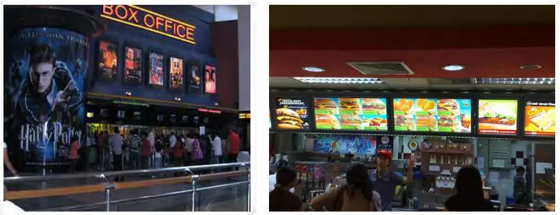
Existing advertisement methods use many papers as shown in Figure 1.2.1. This project can be used as advertisement device since the color will catch the attention of people eyes. Furthermore, there is no need to chop tree to make paper, this VGA Controller only needs new data to change to other design display. Thus, indirectly the environment can be saved.
Figure 1.2.1: The use of paper as poster at cinema and menu at restaurant.
Apart from that, power consumption, weight, price and easy maintenance are main issues in display. PC is heavy to be lift here and there. Therefore, it is not suitable for display. Even though laptop, tablet PC or PDA can be a solution for weigh issues, prices become the next issues. Other than that, PC based device need software and software need license such as operating system. License for software add more cost. So, PC based is not suitable for standalone device that can display at monitor.
1.3 Scope of Work
4
DE2-115 Development and Education Board to generate images on LCD screen, and establish an interconnection between a LCD screen and Altera DE2-115 Development and Education Board to display image.
1.4 Methodology
To design VGA Controller on Verilog compiler software, the block diagram for VGA Controller is created. To implement VGA Controller program into FPGA, the designed VGA Controller is compiled, ran and simulated. If everything goes in the right path, the VGA Controller program will be burned into Altera DE2-115 Development and Education Board. A VGA cable is used to establish an interconnection between a LCD screen and Altera DE2-115 Development and Education Board. One end of the cable is connected to VGA port on Altera DE2-115 Development and Education Board and the other end is connected to VGA port on LCD screen. More detail explanation and flow chart for the design and implementation of VGA Controller on FPGA will be discussed in Chapter III, Methodology.
1.5 Summaries of Chapters
This report is documentary delivering the ideas generated, concepts applied, activities done, and finally the product of the project itself. It consists of five chapters. Following is a chapter-by-chapter description of information in this report.
5
Chapter 2 is a literature review on theoretical concepts applied in this project. This chapter will be discussing the background study of Field-Programmable Gate Arrays (FPGAs), Altera DE2 Development and Education Board, Video Graphics Array (VGA) Controller and Verilog HDL. The theory and concept are explained in this chapter.
Chapter 3 introduces the methodology of the project. This chapter contains flow chart which explains the overall method taken along the project carry out.
Chapter 4 will be covered all the simulation, result, and collection of the data and analysis.
6
CHAPTER II
LITERATURE REVIEW
This chapter is a literature review on theoretical concepts applied in this project. As this project involved FPGAs, Altera DE2-115 Development and Education Board, VGA Controller, Verilog HDL, and Altera Quartus II Compiler Software information on the basic of the above mentioned has to be studied.
2.1 Field-Programmable Gate Arrays (FPGAs)
7
standard parts, they are not designed for any particular function but are programmed by the customer for a particular purpose [5].
FPGAs have compensating advantages, largely due to the fact that they are standard parts. There is no wait from completing the design to obtaining a working chip. The design can be programmed into the FPGA and tested immediately. Apart from that, FPGAs are excellent prototyping vehicles. When the FPGA is used in the final design, the jump from prototype to product is much smaller and easier to negotiate. Also, the same FPGA can be used in several different designs, reducing inventory costs [5].
2.1.1 FPGAs vs. Programmable Logic Devices (PLDs)
In comparison between FPGAs and PLDs, PLDs contain a relatively limited number of logic gates, and the functions they can be used to implement are much smaller and simpler. Moreover, PLDs use fixed interconnect and simply change the logic functions attached to the wires. FPGAs, in contrast, require programming logic blocks and connecting them together in order to implement functions.
2.1.2 FPGAs vs. Application-specific Integrated Circuits (ASICs)
In comparison between FPGAs and ASICs, the final design for ASICs is “frozen in
silicon”, which means it cannot be modified without creating a new version of device. On
8
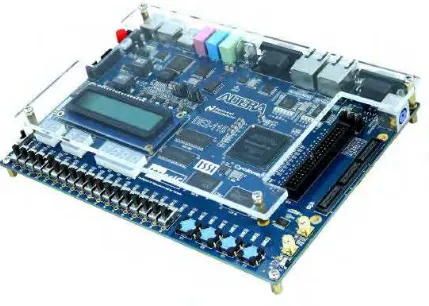
2.2 Altera DE2-115 Development and Education Board
The Altera DE2-115 Development and Education board was designed by professors, for professors. It is an ideal vehicle for learning about digital logic, computer organization, and FPGAs. Featuring an Altera Cyclone® IV 4CE115 FPGA, the DE2-115 board is designed for university and college laboratory use. It is suitable for a wide range of exercises in courses on digital logic and computer organization, from simple tasks that illustrate fundamental concepts to advanced designs [6].