i
“ I hereby declare that I have read through this report entitle “Voltage Dip Mitigation by Controlling Voltage and Current DQ Components” and found that it has comply the partial fulfillment for awarding the degree of Bachelor of Electrical Engineering (Control, Instrumentation and Automation)”
Signature : ...
Supervisor’s Name : MOHAMED AZMI BIN SAID
ii
VOLTAGE DIP MITIGATION BY CONTROLLING VOLTAGE AND CURRENT
DQ COMPONENTS
SYARIFAH SYAKILA BINTI SYED WAHAB
A report submitted in partial fulfillment of the requirement for the degree of
Bachelor of Electrical Engineering (Control, Instrumentation and Automation)
Faculty of Electrical Engineering
UNIVERSITI TEKNIKAL MALAYSIA MELAKA
iii
I declare that this report entitle “Voltage Dip Mitigation by Controlling Voltage and Current DQ Components” is the result of my own research except as cited in the references. The report has not been accepted for any degree and is not concurrently submitted in candidature of any other degree.
Signature : ...
Name : SYARIFAH SYAKILA BINTI SYED WAHAB
iv
Specially dedicated:
To my beloved mother Muziah binti Ahmad,
My beloved sisters,
My supervisor and all my lecturers
And all my friends
For their encouragement, support and motivation
v
ACKNOWLEDGEMENT
Alhamdulillah, I am greatly indebted to Allah SWT on His mercy and blessing for making this project successful.
I would like to take this opportunity to express my profound gratitude and deep regards to my honorable supervisor, Encik Mohamed Azmi bin Said for his exemplary guidance, monitoring and constant encouragement throughout my study. The blessing, help and guidance given by him time to time shall carry me a long way in the journey of life on which I am about to embark.
vi
ABSTRACT
vii
ABSTRAK
viii
TABLE OF CONTENTS
CHAPTER TITLE PAGE
ACKNOWLEDGEMENT v
ABSTRACT vi
ABSTRAK vii
LIST OF FIGURES x
1 INTRODUCTION
1.1 Motivation 1
1.2 Problem Statement 2
1.3 Objectives 2
1.4 Scope Of Research 3
2 LITERATURE REVIEW
2.1 Background Of Project
2.1.1 Voltage Dip Definition 4
2.1.2 Transformation Of Three Phase Reference Frames To Rotating Reference Frame
4
2.1.3 Control System 8
2.1.4 PI Controller 9
2.1.5 Advantage Of PSCAD software 10 2.2 Related Previous Works
2.2.1 Solutions to Voltage Dip 11 2.2.2 Shunt-Connected Voltage Source Converter (VSC) 11
2.2.3 Phase-Locked Loop 12
2.2.4 Mathematical Model And Control Strategy On DQ Frame For Shunt Active Power Filters
ix
2.2.5 DSTATCOM 13
2.2.6 Dynamic Voltage Restorer (DVR) 14 2.3 Summary
2.3.1 Summary Of Background Of Project 17 2.3.2 Summary Of Related Previous Works 16
3 METHODOLOGY
3.1 Research
3.1.1 Voltage Dip Mitigation 18 3.1.2 Method Of Mitigating Power Line Voltage Dip By
Using Current And Voltage DQ component
21
3.1.3 Simulation Of Voltage Dip Mitigation 22
4 RESULTS AND DISCUSSION
4.1 Simulation Results
4.1.1 Process Timeline 31
5 CONCLUSION AND RECOMMENDATION
5.1 Conclusion 41
5.2 Recommendation 42
x
LIST OF FIGURES
FIGURE TITLE PAGE
2.1 Waveform of voltage dip 4
2.2 Block diagram of Clarke’s and Park’s transform 5
2.3 Clarke’s transformation 5
2.4 Park’s transformation 7
2.5 Graph and polar form of three phase reference frames signal, two phase reference signal and rotating reference frame signal
8
2.6 Basic closed loop control system 9 2.7 Block diagram of the implemented control system 12 2.8 Simplified system diagram of a DSTATCOM 14
2.9 Circuit diagram of DVR 15
2.10 Flow chart of feed forward control technique for DVR based on DQO transformation
16
3.1 Flowchart of mitigating voltage dips process 19, 20 3.2 The three phase reference frames signal graph 21 3.3 The rotating reference frame signal graph 22
3.4 System without voltage dip 22
3.5 Vo block 23
3.6 Vαblock 23
3.7 Vβ block 24
3.8 Vd block 24
3.9 Vq block 24
3.10 PLL block 25
3.11 PI controller 26
xi
3.13 Vβ block 27
3.14 Va block 27
3.15 Vb block 27
3.16 Vc block 28
3.17 Simulation with voltage dip 29
3.18 Reactive current injected 30
4.1 Process timeline diagram 31
4.2 Line voltage of three phase component 32
4.3 Line voltage of DQ component 32
4.4 Error voltage without and with PI controller 33
4.5 Steady state response 34
4.6 Line voltage when PI controller is activated before signal is stable
35
4.7 Line voltage when PI controller is activated after signal is stable
35
xii
LIST OF TABLE
TABLE TITLE PAGE
3.1 System parameters used in the simulation model 30 4.1 Settling time of line voltage 33 4.2 Difference between error voltage without and with PI
controller
34
1
CHAPTER 1
INTRODUCTION
1.1 MOTIVATION
Consumer of large electrical power such as industrial is concern about power quality problem. The common power quality problem happen is voltage dip, voltage swell and interruptions. Among of this power quality problem, voltage dip is the most common disturbance occurred. Generally, voltage dip is the decreasing of voltage in short period.
2
1.2 PROBLEM STATEMENT
In power system, the voltage dip usually happens in transmission line and distribution system. Voltage dips is caused by different event that can occur in the power system such as transformer energizing, high starting current and sudden high current that lead to ground fault (current leakage to the earth). One of the situations that caused voltage dip to be produced is, as in industrial application, starting large motor yields a very high current. Based on Ohm’s law, high current is affected on the decreasing of voltage. The decreasing of voltage in this situation is called as voltage dip.
Ideally, power distribution system should provide their customers with an uninterrupted flow of energy at smooth sinusoidal voltage at the contracted magnitude level and frequency. However, in real life, power systems have numerous non linear signals, which significantly affect the quality of power supplies [2]. Therefore, the source of voltage dips problems is unavoidable. So it is important to find a way to overcome voltage dips. Power system analysis is needed to gain some knowledge about how to maintain the level of voltage even there is fault occur.
1.3 OBJECTIVES
There are three main objectives of this project which are:
1. To design a method of mitigating power line voltage dip by using current and voltage DQ components through transforming three phase reference frames to rotating reference frame.
2. To simulate voltage dip mitigation system by using PSCAD software.
3
1.4 SCOPE OF RESEARCH
The power quality problem can be categorized into nine which is voltage dips, voltage swells, harmonics, frequency deviations, transients, unbalance, flicker, interruptions and waveform distortion. Amongst of all this power quality problem, the voltage dips is the only power quality problem that will be focused on.
There are two types of three phase system which is balanced system and unbalanced system. The balanced three phase system is chosen to be the type of system to be tested by voltage dips.
To analyze and simplify the three phase system, there are several method can be used. The method that will be used in this project is DQ transformation.
To mitigate voltage dips, one of the solutions is by injecting reactive power into transmission line. There are several methods to inject reactive power into transmission line. The proposed method is by controlling shunt current DQ component. To controlling shunt current DQ component, the custom power devices used is current source. Current source can be injected in two ways which is series connection and shunt connection. This study will focus on mitigate voltage dips by injecting shunt current source.
4
CHAPTER 2
LITERATURE REVIEW
2.1 BACKGROUND OF PROJECT
2.1.1 Voltage Dip Definition
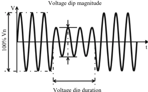
Voltage dip is the decreasing between 0.1 to 0.9 pu in the RMS voltage at the power frequency with duration from 0.5 cycles to 1 minute [4]. For more understanding, voltage dip is visualized as Figure 2.1.
Figure 2.1: Waveform of voltage dip
2.1.2 Transformation Of Three Phase Reference Frames To Rotating Reference Frame
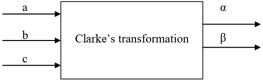
Three phase reference frame signal can be transformed into rotating reference frame signal [5]. One of the method signal transformation can be used is Clarke’s and Park’s transformation. Clarke’s and Park’s transformation is mathematical transformation that rotates the reference frame of three-phase systems in order to simplify the analysis of three-phase circuits. Clarke’s and Park’s transformation transform signal by cascade as
5
Figure 2.2. In other word, to transform three phase reference frame signal into rotating reference signal, the Clarke’s and Park’s transformation is work in separate way.
Figure 2.2: Block diagram of Clarke’s and Park’s transform
Clarke’s transform is transformation three phase stationary parameter from a-b-c system into two phase stationary reference frame as Figure 2.3. The variable of two phase stationary reference frame is called as α and β.
Figure 2.3: Clarke’s transformation
The three phase stationary parameter from a-b-c system is transform into two phase stationary reference frame based on the equation below:
= αβ . [ ] (2.1)
Where;
F : Parameter such as voltage, current, line leakage.
: Parameter such as voltage, current, line leakage in abc form.
a b c
6
αβ from equation (2.1) is obtained as below:
αβ
(2.2)
After simplify the equation (2.1), the equation of two phase stationary reference frame is as below:
α = - ( - ) (2.3)
β = (2.4)
= (2.5)
The equation of inverse Clark’s transformation is as below:
= α (2.6)
= α β (2.7)
= α β (2.8)
7
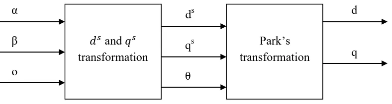
Figure 2.4: Park’s transformation
The three phase stationary parameters is transform into two phase orthogonal stationary reference frame based on the equation below:
(θ) = (θ) . [ αβ ] (2.9)
: Parameter such as voltage, current, line leakage.
from equation (2.9) is obtained as below:
θ θ
θ θ (2.10)
To transform three phase stationary parameters into two phase orthogonal rotary reference frame, the equations involve are:
= α + β (2.11)
= α β (2.12)
α β
o
ds qs θ
d and
transformation
Park’s
8 The equation of inverse Park’s transformation are as below:
α = (2.13)
β = (2.14)
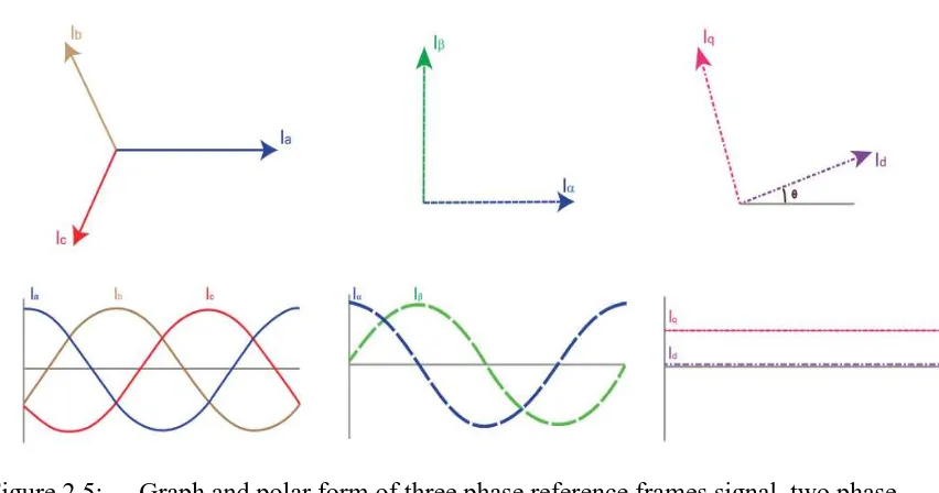
The difference between three phase reference, two phase reference and rotating reference frame that produced from Clarke’s and Parks transform is demonstrated in Figure 2.5.
Figure 2.5: Graph and polar form of three phase reference frames signal, two phase reference signal and rotating reference frame signal
2.1.3 Control System
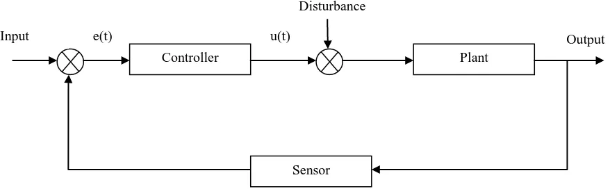
To gain better understanding on the project, the control system of power system should be studied. Figure 2.6 show the basic closed loop control system. In this project, the block plant represents the power system. The power system is consists of generator, transmission line or distribution system. The disturbance represents the fault (voltage dip). The block controller is a feedback controller, such as P controller, PI controller, PD controller or PID controller.
The process in closed loop control system is as follows. When the plant is experience fault, the sensor will sense the amount of output signal is not equal to the
9
desired output signal. Then the output signal will be compared to the reference signal by controller. The controller will process the signal and compensate the signal.
Figure 2.6: Basic closed loop control system
2.1.4 PI Controller
The combination of proportional gain and integral gain is called as PI-controller. The PI-controller is expressed in the equation that contains proportional gain and integral gain as Equation 2.15:
u(t) = Kp e(t) + Ki dt (2.15)
Kp: Proportional gain Ki: Integral gain
From the Equation 2.15, Kp and Ki are the tuning knobs. To obtain the desired output, this tuning knob is adjusted. The function of Kp is to increase the speed of Output
Controller Plant
Sensor Disturbance Input
(reference)
10
2.1.5 Advantage Of PSCAD Software
11
2.2 RELATED PREVIOUS WORKS
2.2.1 Solutions To Voltage Dip
To improve voltage dip in industrial plant, first action is find which process in the plant is sensitive to voltage dip [7]. Then understand the product manufacturing process and operation of the equipment. Next step is identifying which equipment is critical to the other machine operation and will be adversely affected by voltage dip. The example of equipment is Adjustable Speed Drive (ADS) and control and logic circuit. The methods to repair the voltage dip on ADS are reprogramming the response of ADS and restart the motor after a user-defined time delay. While the methods to improve voltage dip on control and logic circuit are use Semi F47 compliant power source, change the trip setting of control circuit and install a coil hold-in device.
Phase of power is categorized into two, which is single phase power and three phase power. To mitigate voltage dip that happens in single phase power and three phase power, consumer should use power conditioning devices. The example of single phase power conditioning devices that available in market is Uninterruptible Power Supply (UPS), Constant Voltage Transformer (CVT), Dip Proofing Inverter, Voltage Dip Compensator (VDC), Dynamic Compensator (Dynacom) and Dynamic Sag Corrector (DySC). The example of three phase power conditioning devices that available in market is Active Voltage Conditioner (AVC), Datawave, Flywheel, Dynamic Voltage Restorer (DVR), three phases Dynamic Compensator (Dynacom), Dynamic Sag Corrector (ProDysc) and Dynamic Sag Corrector (MegaDysc).
2.2.2 Shunt-Connected Voltage Source Converter (VSC)
12
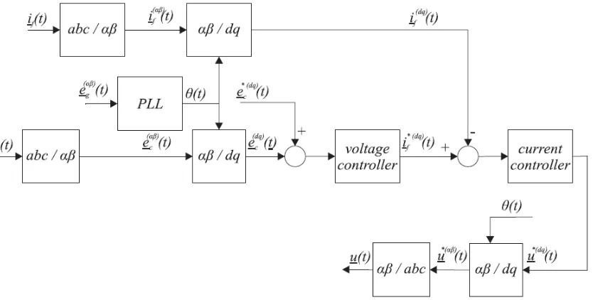
The three phase system can be expressed by two-phase system by obtain the DQ components. The block diagram of the transformation is as Figure 2.7. The purpose of transformation of three phase system into two-phase system is because to facilitate the PI controller to sense the amount of fault in the line voltage. To get the DQ components, voltage and current will be converted to fixed coordinate and then to DQ components. To calculate DQ components, it is important to carry out the calculation of transformation angle θ(t). The transformation angle θ(t) will be calculated by Phase-Locked Loop (PLL).
Figure 2.7: Block diagram of the implemented control system
2.2.3 Phase-Locked Loop