ANALOGUE ELECTRONIC TRAINER (OPERATIONAL AMPLIFIER)
NUR HASNATULAINI BINTI JALANI
This report is submitted in partial fulfillment of the requirement for the award of Bachelor of Electronic Engineering (Industrial Electronics)
Faculty of Electronic and Computer Engineering UniversitiTeknikal Malaysia Melaka (UTeM)
UNIVERSTI TEKNIKAL MALAYSIA MELAKA
FAKULTI KEJURUTERAAN ELEKTRONIK DAN KEJURUTERAAN KOMPUTER
BORANG PENGESAHAN STATUS LAPORAN PROJEK SARJANA MUDA II
TajukProjek : ANALOGUE ELECTRONIC TRAINER
(OPERATIONAL AMPLIFIER)
SesiPengajian : 1 4 / 1 5
Saya NUR HASNATULAINI BINTI JALANI
mengakumembenarkanLaporanProjekSarjanaMudainidisimpan di
Perpustakaandengansyarat-SULIT* *(Mengandungimaklumat yang berdarjahkeselamatanataukepentingan Malaysia seperti yang termaktubdi dalam AKTA RAHSIA RASMI 1972)
TERHAD** **(Mengandungimaklumatterhad yang telahditentukanolehorganisasi/badan di manapenyelidikandijalankan)
TIDAK TERHAD
Disahkanoleh:
__________________________ ___________________________________ (TANDATANGAN PENULIS) (COP DAN TANDATANGAN
PENYELIA)
iii
“I hereby, declared this report entitle “Analogue Electronic Trainer designed for operational amplifier” is the result of my own work except for quotes as cited in the references”
Signature: ……….. Author: NUR HASNATULAINI BINTI JALANI
iv
“I hereby declare that I have read this report and in my opinion, this report is sufficient in terms of the scope and quality for the award Bachelor of Electronic
Engineering (Industrial Electronics)”
Signature: ………. Supervisor Name: FARID ARAFAT BIN AZIDIN
v
vi
ACKNOWLEDGEMENT
In the name of Allah, the Most Gracious, the Most Graceful. I would like to express my sincere gratitude to Him for giving me the strength, health and ability to complete my project Of “ANALOGUE ELECTRONIC TRAINER DESIGN FOR OPERATIONAL AMPLIFIER” and complete this report within the given time period.
I also would like to extend my gratitude to my supervisor, En. Farid Arafat Bin Azidin. For his concerned, kindness, advised and helped to make sure my project is done nicely. Without his guidance from the beginning until the completion of this report, the progress of this project may stuck and cannot be done and documented success.
vii
ABSTRACT
viii
ABSTRAK
ix
CONTENTS
CHAPTER TITLE PAGE
TITLE OF PROJECT i
REPORT VERIFICATION STATUS FORM ii
x
2.3 Type of Training System in the Marketplace 11
xi
4.1 Prototype designed 36
4.2 Simulation result 37
4.3 Input voltage from Traco power 42
4.4 Experimental result 43
4.5 Analysis the result 48
V CONCLUSION AND RECOMMENDATION 51
5.1 Conclusion 52
5.2 Recommendation 53
REFERENCES 54
APPENDICES 55
APPENDIX A 55
APPENDIX B 57
xii
LIST OF FIGURE
NO TITLE PAGE
Figure 1.1 Size the of trainer 4
Figure 2.1 Inverting Amplifier Circuit 8
Figure 2.2 Non-Inverting Amplifier 8
Figure 2.3 Summing Amplifier Circuit 9
Figure 2.4 Difference Amplifier Circuit 10
Figure 2.5 Cascade Operational Amplifier Circuit 11
Figure 2.6 Operational Amplifier Fundamental Trainer 11
Figure 2.7 Training system Design 12
Figure 2.8 Operational Amplifier Type-741 13
Figure 2.9 Operational Amplifier Training System 13
Figure 2.10 Trainer Design and Trainer Case 14
xiii
Figure 3.2 Process flow to get the value of Vo from the theoretical 24 Figure 3.3 Process flow to find the Vo during experimental 25 Figure 3.4 Process flows to get the output waveform in oscilloscope 26
Figure 3.5 Design overview of trainer 28
Figure 3.6 Material Use 28
Figure 3.7 Schematic diagram 29
Figure 3.8 Import the schematic to PCB program 30
Figure 3.9 Layout the PCB 30
Figure 4.3 Output waveform of inverting amplifier circuit 38
Figure 4.4 Non-inverting amplifier 38
Figure 4.5 Output waveform of non-inverting amplifier in multisim 39 Figure 4.6 Summing amplifier 39
Figure 4.7 Output waveform of summing amplifier in multisim 40 Figure 4.8 Different amplifier 40
xiv
Figure 4.10 Cascade Amplifier 41
Figure 4.11 Output waveform of cascade amplifier in multisim 42
Figure 4.12 Positive input voltage 42
Figure 4.13 Negative input voltage 43
Figure 4.14 The Vrms value of inverting amplifier circuit 43 Figure 4.15 Output waveform of inverting amplifier in oscilloscope 44 Figure 4.16 The Vrms value of the non-inverting amplifier circuit 44 Figure 4.17 Output waveform of non-inverting amplifier in oscilloscope45 Figure 4.18 The Vrms value of summing amplifier circuit 45 Figure 4.19 Output waveform of summing amplifier in oscilloscope 46 Figure 4.20 Vrms value of different amplifier circuit 46 Figure 4.21 Output waveform of different amplifier in oscilloscope 47 Figure 5.1 Storage of trainer and all component 52
xv
LIST OF TABLE
NO TITLE PAGE
Table 2.1 Pin connection in Traco Power 17
Table 3.1 Budget of trainer 22
xvi
LIST OF SYMBOLS
xvii
LIST OF APPENDICES
NO TITLE PAGES
APPENDIX A LM 741 Operational Amplifier 55
APPENDIX B Traco Power for DC/DC converter 57
1
CHAPTER I
INTRODUCTION
2
1.1 Project Background
Operational Amplifier (Op-Amp) Trainer has been designed to study the following basic linear amplifier which is inverting amplifier, non-inverting amplifier, summing amplifier, the difference amplifier, and cascade amplifier. The IC 741 used to design the basic circuit of op-amp. The base trainer designed is an open board style. The component was designed as a portable plug in component with its adapter. There have two input voltage which is +/- 15V and +/- 12V. +/- 15V get from the Traco power with high efficiency up to 81%. And +/- 12V get from designed a voltage regulator. In addition the Printed Circuit Board (PCB) in this trainer can be changed to another circuit board which is Bipolar Junction Transistor (BJT) circuit and Field Effect Transistor (FET) circuit. This base trainer design is user friendly for students, lecturers and technicians.
1.2 Problem Statement
3
1.3 Objective of Project
The aim of this project is to design analogue electronic trainers for operational amplifier. In order to achieve that, the following objectives need to be achieved.
1.3.1 To develop a multi design of analogue electronic operational amplifier circuit. The circuit design covers four basic operational amplifier which is inverting amplifier and non-inverting amplifier that include the summing amplifier, difference amplifier and also cascade amplifier.
1.3.2 To model a trainer that is user friendly and can be replace the component easily when its malfunction. The value of the component like resistor can be changed by the lecturer during the experiment conducted. When the component is damaged, technician, no need to take for a long time to replacing the component because this trainer used the plug-in model.
1.3.3 To reduce the space in storing for 3 sets of laboratory experiment which are bipolar junction transistor, field-effect transistor and operational amplifier with using one base training system. In addition, the laboratory shows the good management and organized.
1.4 Scope of Project
4
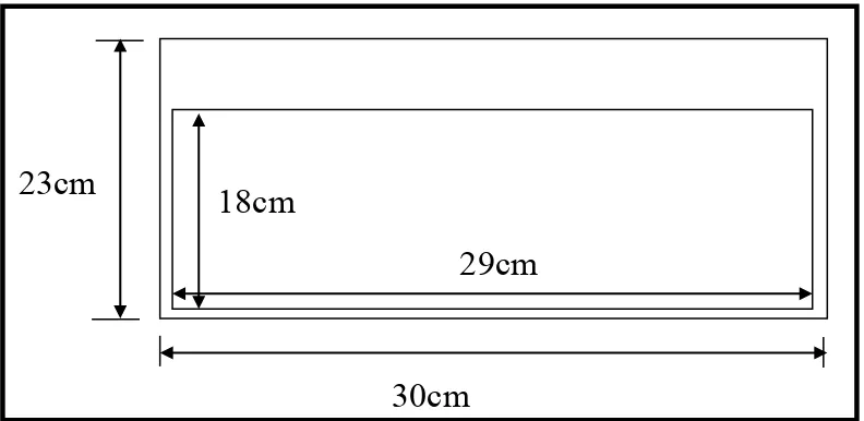
and the circuit designed, there has two software are used which is MultiSim software to simulate the circuit design for operational amplifier and Proteus Software to design and construct the PCB. PCB board is applied for all the circuit implementation. The PVC material has been chosen for the prototype design. The size of the trainer is 23cm wide, 30cm length and 8.5 cm height. The figure below is the size of the base trainer and the trainer design.
Figure 1.1: Size of the trainer
1.5 Importance of Work
The purpose of this project is to design an open board style for the operational amplifier circuit. The operational amplifier circuit design included inverting amplifier, non-inverting amplifier, summing amplifier, difference amplifier and cascade amplifier. This project also proposes to design a base trainer that can be applied to Bipolar Junction Transistor (BJT), Field Effect Transistor (FET) and Operational Amplifier (Op-Amp) during the experiment in lab sessions.
30cm
23cm
18cm
5
1.6 Report Structure
Chapter 1: Describes as a background, problem statement, objectives, scope
project, and the importance of this project.
Chapter 2: Project’s background is discussed. The information about the project
from different resources is discussed in this chapter.
Chapter 3: Describes the methodology of this project, which includes the design
specification and procedure form in the flow chart process.
Chapter 4: Presents the simulation and measurement results. The results
obtained are analyzed and discussed.
Chapter 5: The last chapter concludes the report and recommendations for the
6
CHAPTER II
LITERATURE REVIEW
7
2.1 Ideal operational amplifier
Operational Amplifier is a very high gain differential amplifier with high input impedance and low output impedance. The input impedance is infinite condition which is no current flows into either input of the operational amplifier. While, for the output impedance is zero condition. The operational amplifier can use for any voltage to drive any load impedance. In addition, the bandwidth is in fine condition. When the input difference is zero, the output voltage must be zero.
2.2 Basic operational Amplifier
Operational Amplifier contains two input terminals and one output terminal. The two input terminals are labelled positive and negative, which is non-inverting and inverting, respectively.
2.2.1 Inverting Amplifier
As an inverting amplifier, the resistor is connected to the inverting input as shown in the figure below, with output voltage. � and � correspond to the feedback and input resistances, respectively.
� = −��