UNIVERSITI TEKNIKAL MALAYSIA MELAKA
DEVELOPMENT OF WORKHOLDING DEVICE FOR LOADED
PCB ROUTING PROCESS
This report submitted in accordance with requirement of the Universiti Teknikal Malaysia Melaka (UTEM) for the Bachelor Degree of Manufacturing Engineering
(Robotics and Automation) with Honours.
By
MOHD HAFISZUDDIN B MOHD PUAAD
UTeM Library (Pind.1/2007)
UNIVERSITI TEKNIKAL MALAYSIA MELAKA
BORANG PENGESAHAN STATUS LAPORAN PSM
JUDUL:
Development of Workholding Device for Loaded PCB Routing Process
SESI PENGAJIAN: Semester 2 (2008/2009)
Saya Mohd Hafiszuddin B Mohd Puaad mengaku membenarkan laporan PSM / tesis (Sarjana/Doktor Falsafah) ini disimpan di Perpustakaan Universiti Teknikal Malaysia Melaka (UTeM) dengan syarat-syarat kegunaan seperti berikut:
1. Laporan PSM / tesis adalah hak milik Universiti Teknikal Malaysia Melaka dan penulis.
2. Perpustakaan Universiti Teknikal Malaysia Melaka dibenarkan membuat salinan untuk tujuan pengajian sahaja dengan izin penulis.
3. Perpustakaan dibenarkan membuat salinan laporan PSM / tesis ini sebagai bahan pertukaran antara institusi pengajian tinggi.
4. *Sila tandakan (√)
SULIT
TERHAD
TIDAK TERHAD
(Mengandungi maklumat yang berdarjah keselamatan atau
kepentingan Malaysia yang termaktub di dalam AKTA RAHSIA RASMI 1972)
(Mengandungi maklumat TERHAD yang telah ditentukan oleh organisasi/badan di mana penyelidikan dijalankan)
(Mohd Hafiszuddin B Mohd Puaad) Alamat Tetap:
MBP 226 Pt Limbong Jln Temenggong Ahmad 84150 Pt Jawa
DECLARATION
I hereby, declare this thesis entitled “Development of Workholding Device for Loaded
PCB Routing Process” is the result of my own research except as cited in the references.
Signature :……….
Author’s Name :……….
APPROVAL
This report is submitted to the Faculty of Manufacturing Engineering of UTEM as a partial fulfillment of the requirements for the degree of Bachelor of Manufacturing Engineering (Robotics and Automation) with Honours. The member of the supervisory
committee is as follow:
………
Main Supervisor ( En. Ismail B Abu Shah ) Faculty of Manufacturing Engineering
i
ABSTRACT
ii
ABSTRAK
iii
DEDICATION
For everybody in my life that had supported me to finish this project especially my
iv
ACKNOWLEDGEMENT
I would like to thank for Allah, because of His witness and abundance on me to accomplish the project within the time provided. The research has finished as planned. I also would like to thanks to my supervisor, Mr. Ismail B Abu Shah who took his valuable time to offer concrete suggestions, advices, ideas, helps and supports given to complete this Projek Sarjana Muda I. The encouragements and guidances that have been given is really appreciated
v
TABLE OF CONTENT
Abstract i
Abstrak ii
Dedication iii
Acknowledgement iv
Table of Content v
List of Tables ix
List of Figures x
List of Abbreviations xiv
1. INTRODUCTION 1
1.1 Background of Project 1
1.2 Problem Statement 2
1.3 Objective 3
1.4 Scope 3
1.5 Important of Project 3
2. LITERATURE REVIEW 4
vi
2.2 Workholding Device 5
2.2.1 Definition of Jigs and Fixtures 5
2.2.1.1 Jigs 7
2.2.1.2 Fixtures 13
2.3 Printed Circuit Board (PCB) 33
2.3.1 Single-sided PCB 34
2.3.2 Double-sided PCB 35
2.3.3 Dipping Process of Loaded PCB and Its Effect 35
2.3.3.1 PCB Warpage 36
2.4 Depanelization of PCB by Using Routing Process 39
2.5 Summary 41
3. METHODOLOGY 43
3.1 Flow Chart 43
3.1.1 Flow Chart Diagram 44
3.2 Details of Flow Chart 46
3.2.1 Problem Statement 46
3.2.2 Project Planning 46
3.2.3 Literature Review 49
3.2.4 Part Design Review 49
vii
3.2.6 Component Selection and Placement 49
3.2.7 Locating Datum Selection 50
3.2.8 Fastening and Testing 50
3.2.9 Using Strain Gauge 50
3.2.10 Application of Fixture 50
4. RESULT AND ANALYSIS 51
4.1 PCB Design and Characteristic 51
4.1.1 Types of PCB Material 51
4.1.2 Characteristic of PCB 52
4.2 Depanelization Process 53
4.2.1 Loading and Unloading Process 54
4.2.2 Holding Process 54
4.3.4 Pugh Selection Method 59
4.4 3D Modeling of Design 62
viii
4.4.1.1 Dowel-pin-based Modular Fixture 64
4.4.1.2 Vacuum System 65
4.4.1.3 Sliding Base 67
4.4.1.4 Locator 70
4.4.1.5 Supporter 72
4.4.1.6 PCB Support Jig 73
4.4.1.7 PCB Locating Jig 75
4.4.1.8 Vacuum System 75
5. DISCUSSION 78
5.1 Cutting Force 78
5.2 Jamming Analysis 79
5.3 Design Analysis of Dowel-pin-based Modular Fixture 79
5.4 Vacuum Pressure 79
5.5 Pugh Selection Method 80
6. CONCLUSION AND SUGGESTION 81
6.1 Conclusion 81
6.2 Suggestions 82
Reference 83
ix
LIST OF TABLES
2.1 Differences between jig and fixtures 6
2.2 Comparison of T-slot and Dowel-pin-based modular fixtures 33
3.1 Gantt Chart for PSM 1 47
3.2 Gantt Chart for PSM 2 48
x
LIST OF FIGURES
2.1 Principles of Workholding 5
2.2 A jigs guiding the tool, in this case the drill bushing 6 2.3 A fixtures reference the cutting tool, in this case with a set block 7
2.4 Boring jig 7
xi
2.19 Plug height to avoid jamming 22
2.20 Length engagement for chamfered hole 23
2.21 Distance and angle - primitive cases 23
2.22 Distance and angle - degenerate and special cases 27
2.23 The usage cycle of modular fixtures 27
2.24 T-slot and Dowel-pin –based modular fixtures setups example 28
2.25 Dowel-pin based Modular Fixtures 30
2.26 Dowel-pin-based modular fixtures components 30
2.27 A comparison between stiffness of T-slot and dowel-pin fixtures 32
2.28 Cross-section of PCB 34
2.29 Single-sided PCB 34
2.30 Double-sided PCB 35
2.31 Warpage of 1D linear element due to differential thermal expansion of 37 multi-metallic strips
4.2 Location Hole and Cutting point 53
xii
4.11 Workholding device (isometric view) 63
4.12 Workholding device (right view) 63
4.13 Dowel-pin-based modular-fixture 65
4.14 Dowel-pin-based Modular Fixture ( front view ) 65
4.15 Vacuum Pad 67
4.16 Adjustable Bar 67
4.17 Sliding Base for Locator and Support 68
4.18 Sliding Base for Vacuum Pad 69
4.19 Area covered by adjustable component 70
4.20 Jamming analysis 71
4.21 Locator 72
4.22 Supporter 73
4.23 PCB Support Jig 74
xiii
4.25 PCB Locating Jig 75
xiv
LIST OF ABBREVIATION
ESD - Electro-static Discharge DOF - Degree of Freedom
ICT - In-Circuit Test
PCA - Printed Circuit Assembly PCB - Printed Circuit Board
PCBA - Printed Circuit Board Assembly PWB - Printed Wiring Board
1
CHAPTER 1
INTRODUCTION
1.1 BACKGROUND OF PROJECT.
A printed circuit board, or PCB, is used to mechanically support and electrically connect electronic components using conductive pathways, or traces, etched from copper sheets laminated onto a non-conductive substrate. Alternative names are printed wiring board (PWB), and etched wiring board. A PCB populated with electronic components is a printed circuit assembly (PCA), also known as a printed circuit board assembly (PCBA). Depaneling is a process step in high-volume electronics assembly production. In order to increase the throughput of printed circuit board (PCB) manufacturing and surface mount (SMT) lines, PCBs are often designed so that they consist of many smaller individual PCBs that will be used in the final product. This PCB cluster is called a panel or multiblock. The large panel is broken up or "depaneled" as a certain step in the process - depending on the product, it may happen right after SMT process, after in-circuit test (ICT), after soldering of through-hole elements, or even right before the final case-up of the assembly.
2
The two most important parameters of the routing process are: feed rate and rotational speed. They are chosen according to the bit type and diameter and should remain proportional (i.e. increasing feed rate should be done together with increasing the rotational speed).
Routers generate vibrations of the same frequency as their rotational speed (and higher harmonics), which might be important if there are vibration-sensitive components on the surface of the board. The strain level is lower than for other depaneling methods. Their advantage is that they are able to cut arcs and turn at sharp angles and the disadvantage is lower capacity.
Dowel-pin-based modular fixture is one of the modular fixturing available currently other than T-slot-based modular fixture. The dowel-pin-based modular fixtures have been widely applied, in which the connections of fixture components are accomplished by using a dowel pin and tapped hole. Pin holes and tapped holes are precisely machined in a rectangular (or radial) grid pattern on baseplates or other components for locating and fastening other components. The bolt-screw connection is applied to the in fixture component assemblies. As locating the elements are performed by means of dowel pins and holes, the dowel-pin modular fixture is not continuously adjustable, except using adjustable elements.
1.2 PROBLEM STATEMENT
3
cause the warpage of the PCB and therefore, the PCB is not flat. This condition cause the location of the locating support of the workholding jig must be determined properly so that the locating supports of the workholding jig do not exert stress to the PCB.
1.3 OBJECTIVE.
i. To design the work holding jig.
ii. To determine the diameter of the vacuum pad needed based on the cutting forces. iii. To analyze the design of the workholding.
1.4 SCOPE.
The purpose of this project is to develop the workholding jig to hold the PCB for the Automated Router Machine. Other than that, the cutting forces must be determined in order to identify the maximum diameter required for the vacuum pad. Besides, the design of the locating jig must satisfy the condition of easier loading and unloading.
1.5 IMPORTANCE OF STUDY.
4
CHAPTER 2
LITERATURE REVIEW
This chapter will include the definition of the development, definition of workholding device, explanation of jigs, explanation of fixtures, basic requirements of fixturing systems (ensuring positional accuracy of workpiece, ensuring operation of convenience and safety, ensuring productivity in job, batch and mass production, ensuring low production cost, and 12-point locating principle), current flexible fixturing methodologies, definition and explanation of modular fixturing ( T-slot-based and dowel-pin-based), explanation about the printed-circuit board (PCB) and its characteristic, explanation about soldering process, the definition of routing, explanation about stress deformation analysis and strain gauge.
2.1 Definition of Development
5
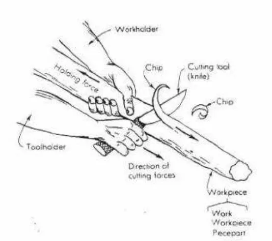
2.2 Workholding Device
Workholding device is all devices that hold, grip, chuck, support and locates a workpiece to perform a manufacturing process. Workholding is also known as jigs and fixtures. In addition to jigs and fixtures, vises, collets, clamps, and other similar devices are also workholders (Leondes, 2000).
Figure 2.1: The principles of workholding
Source: www.mkn.itu.edu.tr
2.2.1 Definitions of Jigs and Fixtures
6
the workpiece must be maintained. To do this, a jig or fixture is designed and built to hold, support and locate every part to ensure that each is drilled or machined within the specific limits (Hoffman, 2003).
The difference between jigs and fixtures can be shown in the Table 2.1 (Adithan and Gupta, 2005).
Table 2.1: Differences between jig and fixtures (Adithan and Gupta, 2005)
Jig Fixture
Jig holds and position the work and locates or guides the cutting tool with respect to the workpiece
Holds and positions the work but does not guide or locate the cutting tool
Jig is not fixed to the machine table
Bolted or clamped to the machine table
Lighter in construction Heavy in construction
Used on drilling, reaming, tapping and couterboring operations
Used for milling, grinding, shaping, planning, boring and welding operations
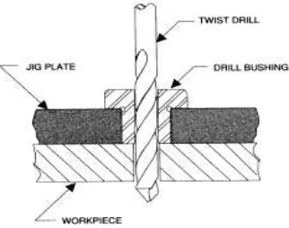
As shown in Figure 2.2, jigs use drill bushings to support and guide the tool. Fixtures, as shown in Figure 2.3, use set blocks and thickness, or feeler, gages to locate the tool relative to the workpiece (Hoffman, 2003).
Figure 2.2: A jigs guiding the tool, in this case the drill bushing