DEVICE SWITCHING USING PC'S PARALLEL PORT
F ARAHIY AH BINTI GHAZALI
This Report Is Submitted In Partial Fulfillment Of Requirements For The Bachelor Degree Of Electronic Engineering (Industrial Electronic)
Faculty of Electronic E ngineering & Computer Engineering Universiti Teknikal Malaysia Melaka
UNIVERSTI TEKNIKAL MALAYSIA MELAKA
FAKULTI KEJURUTE RAAN ELEKTRONIK DAN KEJURUTERAAN KOMPUTER
BORANG PENGESAHAN STATUS LAPORAN
PROJEK SARJANA MUDA II
Tajuk Projek Sesi
Pengajian
DEVICE SWITCHING USING PC'S PARALLEL PORT
2006/2007
Saya ... . ... . .... FARAHfYAH BINTI GHAZALI ... . ... .... ... . .. . ... .... . . ... . . (HURUF BESAR)
mengalcu membenarkan Laporan Projek Sarjana Muda ini disimpan di Perpustakaan dengan syarat-syarat kegunaan seperti berikut:
l. Laporan adalah hakmilik Universiti Te knikal Malays ia Me laka.
2. Perpustakaan dibenarkan membuat salinan untuk tujuan pengajian sahaja.
3. Perpustakaan dibenarkan membuat salinan laporan ini sebagai bahan pertukaran antara institusi pengaji an tinggi .
4 . Sila tandakan (
0 ) :
D
SULIT*D
TERHAD*0
TIDAK T ERHADl
(Me ngandungi maklumat yang berdarjah keselamatan atau ke pentingan Malaysia sep erti yang termaktub di dalam AKT A RAHS IA RASMI 1972)
(Mengandungi maklumat terhad yang tela h ditentuka n o leh organisasi/bada n di ma na pe nyelidikan dijalankan)
D isa hkan oleh:
AN PENULIS) (COP
D
::.fA.Ji:::G:'\
PEI'YEL!A)Ala mat Tetap: BATU 12, KAMPUNG RAMBAI. TOKAI, 06660, ALOR STAR, KE DAH.
Tarikh : .. .
jセ@
.
Nj ッ Nセ@
.. /v.l. ...
sm
HUZAIMAH BT HUSINPensyarah
Fakulti Kej Eletltronik dan Kej kッュ セエ オエ・イ@ (FKEKK), Untversiti Tek,ll<al Malaysia Melaka (UTeM ),
l<arung Beril.und 1200, A.yer l<eroh, 75450 Melaka
111
"I agree that this report is my work except for some summary and information which I
already stated"
Signature
Name
Date
.. .
セG@
..
: F ARAHIY AH BINTI GHAZALI
"I admit that to have read this report and it has follow the scope and quality in Partial
Fulfillment of Requirement for the Degree of Bachelor of Electronic Engineering
(Industrial Electronic)"
Signature
Supervisor 's Name
Date
: . ... . . ...
セセセ@
.. . .. ... .. .: MADAM SIT! HUZAIMAH BINTI HUSIN
: 3o AfR-/.L セッッZZ[M
v
DEDICATION
VI
ACKNOWLEDGEMENT
Vll
ABSTRACT
Vlll
ABSTRAK
Projek ini mencadangkan satu sistem yang boleh mengawal alatan di rumah atau
industri dengan hanya menggunakan sebuah komputer peribadi. Projek pensuisan ini
bermatlamat untuk mengawal pencetak, beban dan peralatan elektrik di rumah yang lain.
Litar untuk proj ek ini terdiri daripada penyahkod, penyongsang, selak, dan bahagian
pemacu geganti. Untuk mengawal kelengkapan tersebut, sistem ini menggunakan liang
selari komputer peribadi. Liang selari komputer peribadi ini adalah sebuah pelantar yang
berkuasa dan efektif untuk melaksanakan projek yang berkaitan dengan mengawal
perkakasan dalam kehidupan sebenar. Aturcara untuk mengawal
kelengkapan-kelengkapan ini ditulis dalam bahasa C. Aturcara komputer melalui litar pengantara akan mengawal geganti, dan kemudian bertindak sebagai suis untuk membuka dan
menutup perkakasan. Seterusnya ia akan disusun menggunakan Penyusun Turbo C.
Selain itu, aturcara perisian membolehkan pengguna untuk mengetahui status semasa
lX
TABLE OF CONTENTS
CHAPTER DESCRIPTION PAGE
PROJECT TITLE
VERIFICATION OF WORK iii
SUPERVISOR'S APPROVAL iv
DEDICATION v
ACKNOWLEDGEMENT vi
ABSTRACT vii
ABSTRAK viii
TABLE OF CONTENTS ix
FIGURE LIST xi
TABLE LIST xii
DIAGRAM LIST xiii
FLOWCHART LIST xiv
LIST OF APPENDIX XV
I INTRODUCTION
1.1 Introduction 1
1.2 Project Objectives 3
1.3 Project Statement 3
1.4 Scope of Work 4
1.5 Project Methodology 4
1.6 Thesis Arrangement 5
II LITERATURE REVIEW
III
IV
v
2.1. 1 Introduction to Parallel Port 2.1.2 Centronics
2.1.3 Parallel Port Address
2.2 IC 74LS154: 4-line to 16-line Decoder I
De-Multiplexer
2.3 IC 74LS74: Dual D-Type Positive-Edge-Triggered Flip-Flops
2.4 IC 74LS05: Hex Inverter
2.5 IC ULN 2803: Octal Peripheral Driver Arrays 2.6 Relay
PROJECT METHODOLOGY 3.1 Introduction
3.2 Project Plan and Requirement 3.3 Circuit Construction
3.4 Flowchart of the Project 3.5 Software Development
RESULT AND PROJECT ANALYSIS 4.1 Expected Result
4.2 Result
4.3 Programming
CONCLUSION AND SUGGESTION 5.1 Discussion and Suggestion 5.2 Conclusion
Xl
FIGURE LIST
CHAPTER FIGURE DESCRIPTION PAGE
II
2.1
Parallel Port Pin Layout 7II
2.2
Logic Symbol for IC 74LS74 18II
2.3
Clock to Output Delays, Data Set-up and Hold 22Times, Clock Pulse Width Waveforms
II
2.4
Set and Clear to Output Delays, Set and Clear 22Pulse Width Waveforms
II
2.5
IC 74LS05 23n
2.6
ULN 2803 25II
2.7
ULN 2803 Pin Layout 26II
2.8
Output and Input Characteristics for ULN 2803 28II
2.9
Relay symbol 28III
3.1
Block diagram for project methodology 31III
3.2
PCB Design using Proteus 32III
3.3
Circuit drawing transition to transparency 33III
3.4
Laminated PCB board with thin film and circuit 33drawing
III
3.5
UV exposure process 34III
3.6
PCB board soaking process 34III
3.7
Etching process 35IV
4.1
Switching Circuit 42IV
4.2
The PCB layout which is design in the Proteus 44software (top view)
IV
4.3
The PCB layout which is design in the Proteus 45xii
TABLE LIST
CHAPTER TABLE DESCRIPTION PAGE
n
2.1 Parallel Port Pin Details 8II 2.2 Data Port Pin's Description 9
II 2.3 Status Port Pin's Description 9
II 2.4 Control Port Pin 's Description 10
II 2.5 Parallel Port Address 14
II 2.6 Function Table for IC 74LS 154 16
II 2.7 Recommended Operating Conditions for 16
IC 74LS154
II 2.8 Electrical Characteristics for IC 74LS154 17
II 2.9 Switching Characteristics for IC 74LS 154 17
n
2.10 Function Table for IC 74LS74 19II 2.11 Recommended Operating Conditions for 20
IC 74LS74
II 2.12 Electrical Characteristics for IC 74LS74 21
II 2.13 Switching Characteristics for IC 74LS74 21
II 2.14 Function Table for IC 74LS05 24
II 2.15 Recommended Operating Conditions for 24
IC 74LS05
II 2.16 Electrical Characteristics for IC 74LS05 24
II 2.17 Switching Characteristics for IC 74LS 154 25
Xlll
DIAGRAM LIST
CHAPTER DIAGRAM DESCRIPTION PAGE
I
1.1
Block Diagram of the System 2I
1.2
Block diagram for main components of the 2switching system
II
2.1
Simplified diagram of the Centronics Protocol 12II
2.2
Connection Diagram for IC 74LS154 15II
2.3
Logic Diagram for IC 74LS74 18II
2.4
Connection Diagram for IC 74LS74 19II
2.5
Connection Diagram for IC 74LS05 23II
2.6
Connection Diagram for IC ULN2803 26CHAPTER FLOW CHART
III 3.1 III 3.2
FLOWCHART LIST
DESCRIPTION
The entire project methodology Project's hardware methodology
XlV
PAGE
36
NO
A
B
c
D
LIST OF APPENDIX
DESCRIPTION
IC 74LS154 data sheet
IC 74LS74 data sheet
IC 74LS05 data sheet
ULN 2803 data sheet
XV
PAGE
52
53
54
CHAPTER I
INTRODUCTION
1.1 Introduction
The PC's parallel port is most commonly used port for interfacing home made
project. The PC's parallel port adapter is specifically design to attach printer with a
parallel port interface, but it can be used as a general input/output port for any device or
appliances that matches its input/output capabilities. The computer program through the
interface circuit controls the relays, which, in turn, switch the appliances on or off.
The parallel port has 12 outputs including 8 data lines and 4 control lines. It can
be used to control up to 255 electrical appliances using only eight data lines from the
parallel port. Besides, this project included the software program that allows the users to
2
Comp uter Program &
OUTPUT Internal
INPUT (appliances
(keyboard) Circuitry ON or
(PC's
Parallel OFF)
Port)
Diagram 1.1: Block Diagram of the System
The block diagram in Figure 1 depicts the main components of the switching system for electrical loads using PC. The control command to switch on/off the
appliances is given through the keyboard. The software program scans the input and as
per the input command, the data is available at the parallel port.
IC 74LSI54 OUT IC 74LS74
IC 74LS05 O.TYPE IC ULN210l RII.AYSAND DECODER
t----1 INVERJfR H fllP.fLOp H RII.AY セ@ IUClRICAL
(LATCH) DRIVIRS APPLIANCES 2
COMPUTER SYSTEM
r
-- - ---
--- - - - -- - ---- ,
I
I
El'iA.BU COMPIJilJ\
2HINO. I rAJ.ro INPliT PRO CRAM I (KIYBO.Wl) H .t INTERN.U. ___, CONNECTOR D4-D7
CIRCUITRY LPTPORT
I I
I
- - ----
___ _____ ___ __
....___, IC 74LSI54 DECODER
I
Diagram 1.2: Block diagram for main components of the switching system
Out of eight bits, first four bits (DO through D3) are data signal bits and the
remaining fo ur bits (0 4 through 0 7) are used as control signals. Control signals are
given to decoder 1. The output of decoder 1 is given to Enable pins of decoders 2. Data
signals are given to decoder 2. The outputs of decoder 2 are inverted and fed to a D-type
3
ULN2803. The relay drivers drive the relays for switching the appliances. But in this
project, I've only used LED to represent as electric appliances .
1.2 Project Objectives
The main objective of this project is to build a switching system that can control
home appliances by only using a single PC and at the same time this system could also
provide convenience and easier lifestyle. This system is not only easy to use but it also
reveals people nowadays using high-technology like using in advanced country. Beside
as a convenient, this control system also provides more safety environment in home.
1.3 Project Statement
In this decade, there are many new technologies which are being implemented in
real world for making life easier. Some of these technologies are expensive but offered a
very good service and there are some cheaper but yet still provide good service for users.
Based on all this aspect, I have come up with this good and acceptable proposed
project. Although it is quite costly but is very efficient in control real world peripheral.
This project is actually provides users a simple life by giving more choices to them. This
switching system allowed users to control home appliances by only using a PC. The
users only need to give control command through PC's keyboard and interface circuit
will send the instruction to the load, which is whether to turn on or to turn off. This
switching system also useful in emergency condition. It can help the user to switch on or
4
1.4 Scope Of Work
The scope of work for this project is mainly about produce a convenience
switching device controlling by only a single port and make a test in order to prove the
efficiency of the project. This device must be able to control the entire load that is
needed by the user. The study of how the parallel port is working and its characteristic
must be done. Since this project is using C language as its software programming, the
study of this language also must be done. Besides, the software programming must be
easy to understand by the user in order to allow them to know the current status of the
loads. This project is involved hardware and software programming, so to make sure this
project work successful, the test must be done before and after combination.
1.5 Project Methodology
The first process in this project is to search and create ideas which are relevant to
the project I'm working with. Then, the next process is to start the literature study on the
project. These are done by referring a number of books and surf the internet which
guided me to retrieve relevant and useful information on this project. The following
process is to design and simulate the project circuit. After the simulation, the circuit is
drawn and PCB layout is printed out. The components then are placed and soldered on
the PCB . The next process is to test and troubleshoot the circuit if there any problem.
Since this project also included software development, the software programming will
be created and tested in the simulation. This project is a complete system when the
5
1.6 Thesis Arrangement
Generally, this thesis comprises five chapters.
Chapter I will describe in general why this project is done.
Chapter II then will discuss related theories with this project. These theories are
useful as comprehension for me to execute this project.
Chapter IV will present the result of this project. Every result will follow by
briefly description to support the result.
Finally, the last chapter will clarify the conclusion for this project. This chapter
CHAPTER II
LITERATURE REVIEW
2.1 Parallel Port
2.1.1 Introduction to Parallel Port
PC's parallel port can be very useful
VO
channel for connecting own circuits toPC. The PC's parallel port can be used to perform some very amusing hardware
interfacing experiments. Parallel port differs from serial ports primarily in that they use
eight pins to carry data instead of just one. When all eight pins are transmitting in
parallel, the computer can send an entire byte in the time that a serial port takes to send 1
bit. The parallel port is traditionally associated with printer connections, but in recent
years, the interface has come to be used to connect external devices.
Computers typically have one parallel port, although system BlOSs support up to
three. The parallel port or line printer terminal (LPT) port is a 25-pin D-type female
connector available at the back of a PC. A basic PC usually comes with one or two LPT
7
D7 D6 DS D4 D3 D2 Dl DO
S7 S6 S5 S4 S3
C3 C2 Cl CO
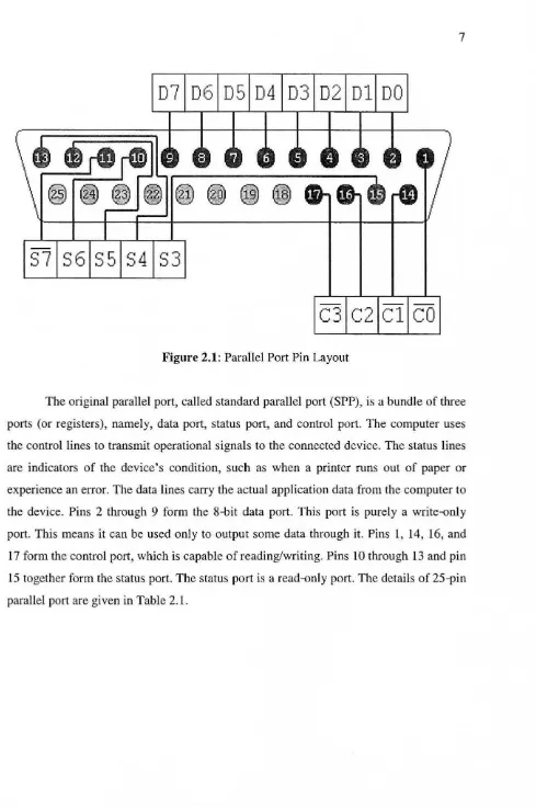
Figure 2.1: Parallel Port Pin Layout
The original parallel port, called standard parallel port (SPP), is a bundle of three
ports (or registers), namely, data port, status port, and control port. The computer uses
the control lines to transmit operational signals to the connected device. The status lines
are indicators of the device's condition, such as when a printer runs out of paper or
experience an error. The data lines carry the actual application data from the computer to
the device. Pins 2 through 9 form the 8-bit data port. This port is purely a write-only
port. This means it can be used only to output some data through it. Pins l, 14, 16, and
17 form the control port, which is capable ofreading/writing. Pins 10 through 13 and pin
15 together form the status port. The status port is a read-only port. The details of 25-pin
[image:22.597.53.542.40.776.2]8
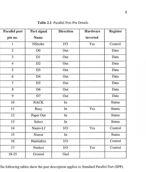
Table 2.1 : Parallel Port Pin Details
Parallel port Port signal Direction Hardware Register
pin no. Name inverted
1 NStrobe 1/0 Yes Control
2 DO Out Data
3 Dl Out Data
4 D2 Out Data
5 D3 Out Data
6 D4 Out Data
7 D5 Out Data
8 D6 Out Data
9 D7 Out Data
10 NACK In Status
11 Busy In Yes Status
12 Paper Out In Status
13 Select In Status
14 Nauto-Lf I/0 Yes Control
15 Nerror In Status
16 Ninitialize I/0 Control
17 Nselect 1/0 Yes Control
18-25 Ground Gnd
[image:23.598.64.541.35.597.2]9
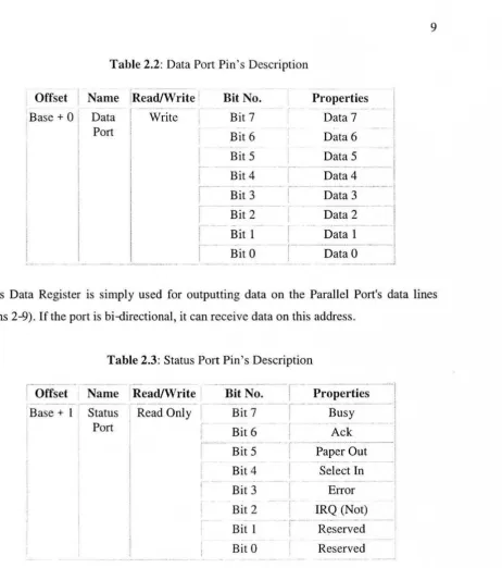
Table 2.2 : Data Port Pin's Description
Offset I
I Name !Read/Write Bit No. Properties
Base+ 0 1 Data I I Write Bit 7 Data 7 I
Port
I
Bit 6 Data 6I
I
Il
Bit 5 Data 5- I
I
I
I
---
-I
Bit 4 Data4
I
i
セMM- - - -
---1
I Bit 3 Data 3
I
I
!
Bit 2 Data 2
I
Bit I
I
Data 1セMM
r· -
MᄋMMᄋ MᄋセM-Bit 0 DataO
I
-
- - - -
---
- -
--This Data Register is simply used for outputting data on the Parallel Port's data lines
[image:24.598.94.538.42.323.2](Pins 2-9) . If the port is bi-directional, it can receive data on this address.
Table 2.3: Status Port Pin's Description
,....---I
-·-I
Offset Name Read/Write Bit No. Properties
-
- -
--
--
-·-
- - - iBase + l Status Read Only Bit 7 Busy I
Port Bit 6 Ack
j
---
- -··----Bit 5 Paper Out
Bit 4 Select In
Bit 3 Error
Bit 2 IRQ (Not)
Bit l rセ ウ・ イカ・、@
Bit 0 Reserved
-
-The Status Port (base address + 1) is a read only port. Any data written to this port will
[image:24.598.77.540.51.573.2]