1
AN IMPLEMENTATION OF FULL-STATE OBSERVER AND
CONTROLLER FOR DYNAMIC STATE-SPACE MODEL OF ZETA
CONVERTER
Hafez Sarkawi1, Mohd Hafiz Jali2
1
Faculty of Electronics and Computer Engineering (FKEKK),
University Technical Malaysia Melaka (UTeM), Melaka
2
Faculty of Electrical Engineering (FKE),
University Technical Malaysia Melaka (UTeM), Melaka
1
[email protected](+606-5552025) and [email protected](+606-5552331)
Abstract
Zeta converter is a fourth order dc-dc converter that can increases (step-up) or decreases
(step-down) the input voltage. The converter needs feedback control to regulate its output
voltage. A full-state observer can be used to estimate the states of the system in condition the
output must be observable. The estimated states can be fed to full-state feedback controller to
control the plant. This paper presents the dynamic model of zeta converter. The converter is
modeled using state-space averaging (SSA) technique. Full-state observer and controller are
implemented on the converter to regulate the output voltage. The simulation results are
presented to verify the accuracy of the modeling and the steady-state performance subjected
2
Keyword: Modeling, zeta converter, SSA technique, full-state feedback controller, full-state
observer
Abstrak
Penukar Zeta adalah penukar dc-dc empat peringkat yang boleh menaik atau menurunkan
voltan masukan. Sesuatu penukar memerlukan pengawal suap-balik untuk mengatur voltan
keluarannya. Pemantau keadaan-penuh boleh digunakan untuk menganggarkan keadaan
dalam sesuatu sistem tetapi dengan syarat keluaran system tersebut boleh dipantau. Keadaan
yang telah dianggarkan tersebut boleh di suap ke perngawal suap-balik keadan penuh untuk
mengawal sesuatu loji. Kertas ini mempersembahkan model dinamik untuk penukar zeta.
Penukar tersebut dimodelkan menggunakan teknik purata ruang-keadaan (PRK). Pemantau
dan pengawal keadaan-penuh diletakkan pada penukar tersebut untuk mengatur voltan
keluaran. Hasil simulasi akan dipersembahkan untuk mengesahkan ketepatan model penukar
tersebut dan sambutan keadaan mantapnya apabila dimasukkan hingar pada masukan dan
beban.
Kata kunci: Pemodelan, penukar zeta, teknik PRK, pengawal suap-balik keadaan penuh,
3
1. Introduction
Zeta converter is fourth order dc-dc converter that can step-up or step-down the input voltage.
The converter is made up of two inductors and two capacitors. Modeling plays an important
role to provide an inside view of the converter’s behavior. Besides that, it provides information
for the design of the compensator. The most common modeling method for the converter is
state-space averaging technique (SSA). Open-loop system has some disadvantages where the
output cannot be compensated or controlled if there is variation or disturbance at the input. For
the case of zeta converter, the changes in the input voltage and/or the load current will cause the
converter’s output voltage to deviate from desired value. This is a disadvantage because when
the converter is used as power supply in electronic system, problem could be happened in such
that it could harm other sensitive electronic parts that consume the power supply. To overcome
this problem, a closed-loop system is required. Full-state feedback controller is one of the
compensator used in closed-loop system. Compared to other compensator such as PID,
full-state feedback controller is time-domain approach which makes the controller design is
less complicated than PID approach which is based on frequency-domain approach. This is due
to the modeling process is based on state-space matrices technique. It is sometimes impossible
to measure certain variables except input and output. Full-state observer can overcome this
issue because it can estimate the states of the system by using input and output measurement
4
2. Modeling of Zeta Converter
2.1 Overview of SSA Technique
State-space averaging (SSA) is a well-known method used in modeling switching converters
[1]. To develop the state space averaged model, the equations for the rate of inductor current
change along with the equations for the rate of capacitor voltage change that are used.
A state variable description of a system is written as follow:
Bu Ax
x (1)
Eu Cx
vO (2)
where A is n x n matrix, B is n x m matrix, C is m x n matrix and E is m x m matrix. Take note
that capital letter E is used instead of commonly used capital letter D. This is because D is
reserved to represent duty cycle ratio (commonly used in power electronics).
For a system that has a two switch topologies, the state equations can be describe as [2]:
Switch closed
Switch open
For switch closed at time dT and open for (1-d)T, the weighted average of the equations are:
u
B
x
A
x
1
1u E x C vO 1 1
u B x A x 2 2
5
(3)
(4)
By assuming that the variables are changed around steady-state operating point (linear signal),
the variables can now be written as:
where X, D, and U represent steady-state values, and , and represent small signal values.
During steady-state, the derivatives ( ’) and the small signal values are zeros. Equation (1)
now becomes:
(6)
BU A
X 1 (7)
while Equation (2) can be written as:
The matrices are weighted averages as:
For the small signal analysis, the derivatives of the steady-state component are zero:
Substituting steady-state and small signal quantities in Equation (5) into Equation (3), the
Ad A d
x
Bd B
d
ux 1 21 1 21
Cd C d
x
Ed E
d
uvO 1 21 1 21
O O
O V v
v
u U u
d D d
x X x
~ ~
~ ~
BU AX
0
EU BU CA
VO 1
D
C D C C
D B D B B
D A D A A
1 1 1
2 1
2 1
2 1
x
x
x
X
x
~
0
~
~
(5)
6 equation can be written as:
If the products of small signal terms can be neglected, the equation can be written as:
or in simplified form,
(9)
Similarly, the output from Equation (4) can be written as:
or in simplified form,
(10)
2.2 Modeling of Zeta Converter By SSA Technique
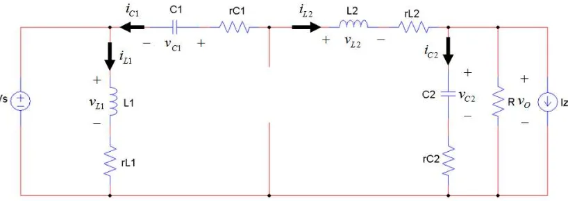
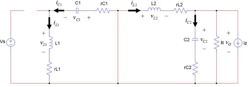
The schematic of zeta converter is presented in Fig. 1. Basically the converter are operated in
two-states; ON-state (Q turns on) and OFF-state (Q turns off). When Q is turning on (ON-state),
the diode is off as shown in Fig. 2.During this state, inductor L1 and L2 are in charging phase.
When Q is turning off (OFF-state), the diode is on as presented in Fig. 3. At this state, inductor
L1 and L2 are in discharge phase. Energy in L1 and L2 are discharged to capacitor C1 and output
part, respectively. To ensure the inductor current iL1 and iL2 increases and decreases linearly on
respective state, the converter must operate in Continuous Conduction Mode (CCM). CCM
A D d A D d
X x
B
D d
B
D d
U u
x ~ 1 ~ ~ ~ 1 ~ ~
~
2 1
2
1
AD A D
x
BD B
D
u
A A
X
B B
U
dx 1 ~ 1 ~ ~
~
2 1 2
1 2
1 2
1
A
A
X
B
B
U
d
u
B
x
A
x
~
~
~
~
2 1 2
1
Cd C d
x
Ed E
d
u
C C
X E E
U
dvO 1 ~ 1 ~ ~
~
2 1 2
1 2
1 2
1
C C X E E U
du E x C
7
means the current flows in inductors remains positive for the entire ON-and-OFF states. Fig. 4
shows the waveform of iL1 and iL2 in CCM mode. To achieve this, the inductor L1 and L2 must
be selected appropriately. According to [3], the formula for selection the inductor values are:
Fig. 1. Dynamic model of zeta converter
Fig. 2. Equivalent zeta converter circuit when Q turns on
D R
D r R r Df
R D
L L C
1 1
2
1 2 2 1
1
R r f
R D
L L2
2 1
8
Fig. 3. Equivalent zeta converter circuit when Q turns off
Fig. 4. iL1 (left) and iL2 (right) waveform in CCM [3]
2.2.1 State-space Description of Zeta Converter
ON-state (Q turns on)
9
OFF-state (Q turns off)
Output voltage equation for both states:
The weighted average matrices for ON-state and OFF-state are:
R r C R r C R C D C D R r L R L D R r L R r Dr r R r L D L r D r A C C C C C C L C L C 2 2 2 2 1 1 2 2 2 2 2 2 1 2 2 1 1 1 1 1 0 0 0 0 1 0 0 1 0 ) 1 (
R r C R R r L R r L D L D B C C C 2 2 2 2 2 2 1 0 0 0 0 R r R R r R r C C C C 2 2 2 0 0 R r R r E C C 2 2 0
Z S C C C C C L L C C C C C L L C C C L L i v R r C R R r L R r L L v v i i R r C R r C R C R r L R R r R r r L L r r L dt dvdt dvdt di dt di 2 2 2 2 2 2 1 2 1 2 1 2 2 2 2 1 2 2 2 2 2 2 1 1 1 1 2 1 2 1 0 0 0 1 0 1 1 0 0 0 0 0 1 0 1 0 0 1 0 1 Z S C C C C L L C C C O i v R r R r v v i i R r R R r R r v 2 2 2 1 2 1 2 22 0 0
10
2.2.2 Zeta Converter Steady-state
U is consisted of two input variables which are VSand IZ. However, for the steady-state output
equation, the goal is to find the relationship between output and input voltage. Thus only
variable VS is used for the derivation. However for IZ multiplication, matrices B and E are
included. For this reason, B and E matrices need to be separated into two matrices; BS, ES(for
input variable VS) and BZ, EZ (for input variable IZ) which are presented as follow:
To get an equation that relates the output and input voltage, the above equation (7) needs to be
modified by replacing U=VS, B=BS and E=ES=0:
or in circuit parameters form [1]:
R r C R R r L R r L D L D B B B C C C Z S 2 2 2 2 2 2 1 0 0 0 0
R r R r E E E C C Z S 2 2 0 S SO CA B V
V 1
11
2.2.3 Zeta Converter Small-signal
Equation (6) is substituted into (9), thus the small signal state-space equation can be written as:
or
where,
in circuit parameters form [4]:
Equation (10) is recalled, the small signal output equation is written as
Since C1=C2 and E1=E2, the equation above is simplified as:
A A A BU B B U
d uB x A
x ~ ~ ~
~
2 1 1
2
1
d B u B x A
x ~ ~ d~
~
A A
A BU
B B
UBd 1 1 2
2
1
0 1 1 1 1 1 1 1 1 1 1 1 1 1 1 1 2 1 1 1 2 1 2 1 1 2 2 Z S Z L C S L Z L S C L L C L d I D R DV C RI Dr D r V r R D L RI Dr V Dr r R D L D D R r D D R r R r D R B
C C X E E U
d uE x C
vO ~ ~ ~
~
2 1 2
1
u E x C
vO ~ ~
12
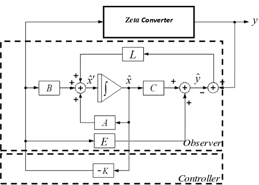
3. Control of Zeta Converter Using Full-state Feedback Controller (FSFBC) and
Observer (FSO)
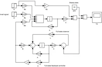
Fig. 5. An estimated full-state feedback controller
3.1FSFBC Based on Pole Placement Technique
Desired poles must be placed further to the left handside (on s-plane) of the system’s dominant poles location to improve the system steady-state error response. A good rule of
thumb is that the desired poles are placed five to ten times further than the system’s dominant
poles location [5]. For the full-state feedback controller, the closed-loop characteristic
equation can be determined by:
0 A BK I
Zeta Converter
Observer
13
3.2FSFBC Based on Optimal Control Technique
To optimally control the control effort within performance specifications, a compensator is
sought to provide a control effort for input that minimizes a cost function:
This is known as the linear quadratic regulator (LQR) problem. The weight matrix Q is an n x
n positive semi-definite matrix (for a system with n states) that penalizes variation of the state
from the desired state. The weight matrix R is an m x m positive definite matrix that penalizes
control effort [3].
To solve the optimization problem over a finite time interval, the algebraic Ricatti equation is
the most commonly used:
where P is symmetric, positive definite matrix and K is the optimal gain matrix that is used in
full-state feedback controller. Since the weight matrices Q and R are both included in the
summation term within the cost function, it is really the relative size of the weights within
each quadratic form which are important [6].
0 x Qx u Ru dt
J T T
0
1
Q
P
B
PBR
P
A
PA
T T14
3.3FSO State Estimation
The output of the estimator can be compared to the output of the system, and any difference
between them can be multiplied with an observer gain matrix L and fed back to the state
estimator dynamics. Basically, the full-state observer has the form [7]:
where z is the difference between output and estimated output.
4. Simulation Model
Table I shows the parameters that are used for the zeta converter circuit. By substituting all
the parameters in the state equations derived previously, the state matrices can be gathered as
presented.
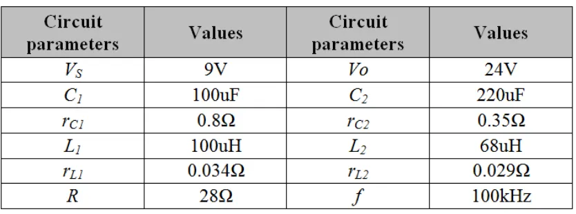
Table I: Zeta Converter Circuit Parameters
Lz
Bu
x
A
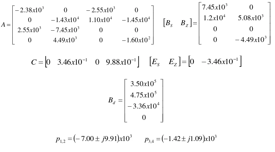
15 2 3 3 3 4 4 4 3 3 10 60 . 1 0 10 49 . 4 0 0 0 10 45 . 7 10 55 . 2 10 45 . 1 10 10 . 1 10 43 . 1 0 0 10 55 . 2 0 10 38 . 2 x x x x x x x x x
A
3 3 4 3 10 49 . 4 0 0 0 10 08 . 5 10 2 . 1 0 10 45 . 7 x x x x B
BS Z
1 1
10 88 . 9 0 10 46 . 3
0
x x
C
ES EZ
0 3.46x101
0 10 36 . 3 10 75 . 4 10 50 . 3 4 5 5 x x x Bd
32 ,
1 7.00 j9.91x10
p
34 ,
3 1.42 j1.09 x10
p
Table II: FSFBC Gain for Various Pole Placement (Top) and Cost Function Weight (Bottom)
16
Fig. 9. Closed-loop zeta converter with full-state observer model
The eigenvalues for the zeta converter system can be calculated. Poles 3x, Poles 5x and Poles
7x refer to the pole location at 3 times, 5 times and 7 times further than the most dominant
eigenvalues that is at -7x10³ (real s-plane). FSFBC gain, K for various pole location and cost function weight are calculated for the closed-loop compensation and are shown in Table II.
Table III on the other hand shows the FSO gain, L for the full-state observer. As for the
Simulink model, the zeta converter open-loop with the implementation of full-state observer
17 5. Results
For the open-loop, when subjected to input voltage disturbance of S=1V, the output
increased significantly to approximately 27V while for load current disturbance of Z=1A, the
output decreased to about 21.6V (Fig. 10). This response to disturbance is very undesirable.
To reduce the effect of the disturbances, full-state feedback controller is used. The controller
is designed based on pole placement and optimal control technique. When subjected to input
disturbance of S=1V, the response is shown in Fig. 11. In the figure, the pole location that
yield the best compensation is Poles 7x with output voltage of 24.006V. while cost function
weight iL22, 100vC22 produced the best compensator with the output voltage of 24.002V for
optimal control technique. On the other hand, when subjected to load current disturbance of
Z=1A, again Poles 7x (23.95V) and iL22, 100vC22 (23.95V) produced the best results as shown
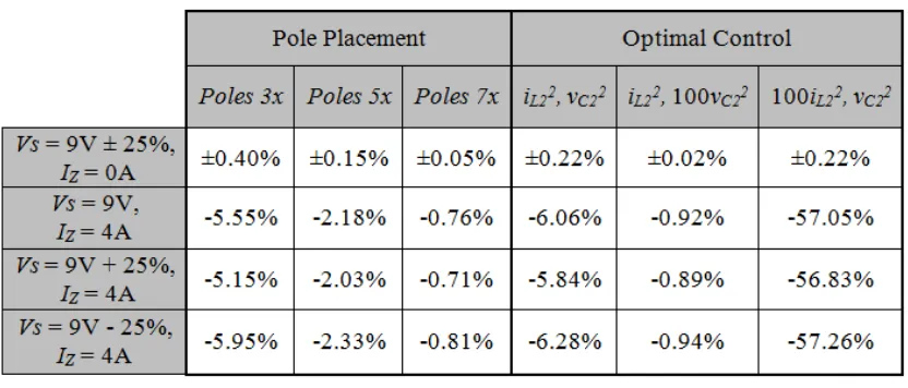
in Fig. 12. Table IV shows the summary of the voltage regulation when subjected to input
voltage disturbance and/or load current disturbance for FSFSC based on pole placement and
optimal control technique. It is required that the VR is ≤ ± 1%. For pole placement technique,
only pole location at Poles 7x can achieve this requirement while for optimal control
technique, iL22, 100vC22 can be used for the output voltage regulation requirement. Since both
pole placement and optimal control technique can achieve required voltage regulation
18
Fig. 10. Open-loop output voltage, VO response to disturbance S=1V (left) and Z=1A (right)
Fig. 11. Compensated output voltage, VO response to disturbance S=1V using FSFBC based
on: pole placement (left) and optimal control technique (right)
Fig. 12. Compensated output voltage, VO response to disturbance Z=1A using FSFBC based
19
Table IV: Output Voltage Regulation Using FSFBC Based On Pole Placement and Optimal
Control Technique Comparison
6. Conclusions
In this paper, modeling and control of a zeta converter operating in Continuous Conduction
Mode (CCM) has been presented. The state-space averaging (SSA) technique was applied to
find the steady-state equations and small-signal linear dynamic model of the converter. To
ensure the output voltage maintain at the desired voltage regulation requirement, full-state
observer and controller are used as the controller. To compensate the output voltage from the
input voltage and load current disturbances, feedback controller gain for Poles 7x and (iL22,
100vC22) is proven to produce the best compensated output voltage for FSFBC based on pole
20
Funding sources
This research is supported by Ministry of Higher Education Malaysia and University Technical
Malaysia Melaka (UTeM), Malaysia under Faculty of Electronics and Computer Engineering
(FKEKK) short-term grant (Ref: PJP/2012/FKEKK(4A)/S01081)
Acknowledgments
The author would like to express gratitude to the Ministry of Higher Education Malaysia and
University Technical Malaysia Melaka (UTeM), Malaysia for the financial support.
References
[1]E.Vuthchhay and C.Bunlaksananusorn, “Dynamic Modeling of a Zeta Converter with State-space Averaging Technique”, Proceedings of ECTI-CON 2008, pp. 969-972, 2008 [2]D.W.Hart, “Introduction to Power Electronics”, Prentice-Hall Inc., 1997
[3]E.Vuthchhay and C.Bunlaksananusorn, “Modeling and Control of a Zeta Converter”,The 2010 International Power Electronics Conference, pp. 612-619, 2010
[4]E.Vuthchhay, C.Bunlaksananusorn and H.Hirata, “Dynamic Modeling and Control of a
Zeta Converter”, 2008 International Symposium on Communications and Information Technologies (ISCIT 2008), pp. 498-503, 2008
[5]Charles L.Philips and H. Troy Nagle; “Digital Control System Analysis and Design”, 1st
Edition, Prentice-Hall Inc., 1984
[6]R.Tymerski and F.Rytkonen, “Control System Design”,
www.ece.pdx.edu/~tymerski/ece451/Tymerski_Rytkonen.pdf, 2012
[7]M.Dahari and N.Saad, “Digital Control Systems –Lecture Notes”,2002
[8]R. W. Erickson and D. Maksimovic, “Fun amentals of Power Electronics”, 2nd Edition., Kluwer Academic Publishers,2001
[9]Ned Mohan, “Power Electronics and Drives”, MNPERE, 2003
[10] Muhammad H. Rashid. “Power Electronics Handbook”, Academic Press, 2001