BOOTH’S ALGORITHM DESIGN USING FIELD PROGRAMMABLE GATE ARRAY
MUHAMMAD SHUKRI BIN OMAR
This Report Is Submitted In Partial Fulfillment of Requirements for the Bachelor Degree of Electronic Engineering (Computer Engineering)
Faculty of Electronic Engineering & Computer Engineering Universiti Teknikal Malaysia Melaka
ii
UNIVERSTI TEKNIKAL MALAYSIA MELAKA FAKULTI KEJURUTERAAN ELEKTRONIK DAN KEJURUTERAAN KOMPUTER
BORANG PENGESAHAN STATUS LAPORAN PROJEK SARJANA MUDA II
Tajuk Projek : BOOTH’S ALGORITHM DESIGN USING FIELD PROGRAMMABLE GATE ARRAY
Sesi Pengajian : 1 3 / 1 4
Saya MUHAMMAD SHUKRI BIN OMAR
mengaku membenarkan Laporan Projek Sarjana Muda ini disimpan di Perpustakaan dengan syarat-syarat kegunaan seperti berikut:
1. Laporan adalah hakmilik Universiti Teknikal Malaysia Melaka.
2. Perpustakaan dibenarkan membuat salinan untuk tujuan pengajian sahaja.
3. Perpustakaan dibenarkan membuat salinan laporan ini sebagai bahan pertukaran antara institusi pengajian tinggi.
4. Sila tandakan ( √ ) :
SULIT* *(Mengandungi maklumat yang berdarjah keselamatan atau
kepentingan Malaysia seperti yang termaktub di dalam AKTA RAHSIA RASMI 1972)
TERHAD** **(Mengandungi maklumat terhad yang telah ditentukan oleh
organisasi/badan di mana penyelidikan dijalankan)
TIDAK TERHAD
Disahkan oleh:
___________________________
(TANDATANGAN PENULIS)
__________________________________
(COP DAN TANDATANGAN PENYELIA)
iii
I hereby declare that this is the result of my own work except for quotes as cited in the references.
Signature :
iv
I hereby declare that I have read this report and in my opinion this report is Sufficient in terms of the scope and quality for the award of Bachelor Degree of
Electronic Engineering (Computer Engineering).
Signature :
v
To my beloved family, my project Supervisor Mr Anuar Bin Jaafar, all the lecturers that involve in my project, my friend and also to all my classmate that has been participated
vi
ACKNOWLEDGEMENT
Assalamualaikum warahmatullahi wabarakatuh,
Thank you Allah forgives me this opportunity to finish my undergraduate project. It is a very great pleasure for me to acknowledge the contribution of a large number of individuals that being supportive throughout this year. First of all, I would like to thank my supervisor, Mr Anuar Bn Jaafar, for provide me precious helps, supports and motivation throughout the development of this project. I would like to dedicate appreciation to my friends and course mates. We have gone through thick and thin together. All the courage and valuable memory you gave will never be forgotten. Thank you for always being by my side. I also would like to acknowledge my parents and siblings. Thank you for your support and motivation. I am gratefully acknowledged the support, encouragement, and patience of my families. I am very happy to have family that always loves me and care about me. Without them, I will not be able to finish this project. Last but not least to all other peoples whose are not mention here. Your contributions are very much appreciated.
vii
ABSTRACT
viii
ABSTRAK
ix
TABLE OF CONTENTS
CHAPTER CONTENT PAGE
PROJECT TITLE i
REPORT VERIFICATION ii
APPROVAL iii
DEDICATION v
ACKNOWLEDGEMENT vi
ABSTRACT vii
ABSTRAK viii
TABLE OF CONTENTS ix
LIST OF FIGURES xii
LIST OF TABLES xv
LIST OF ABBREVIATIONS xvii
LIST OF APPENDIXS xvi
I INTRODUCTION 1.1 Project Overview 1
1.2 Problem Statement 2
1.3 Objective 2
1.4 Project Scope 3
1.5 Thesis Overview 3
II LITERATURE REVIEW 2.1 Introduction 4
2.2 Booth's Algorithm 4
x
2.4 FPGA Implementation of an Adaptive Hearing 6
Aid Algorithm using Booth‟s Wallace Multiplier 2.4.1 Hearing Aid Architecture 6
2.4.2 Multiplier Background 7
2.4.3 Partial Product Generation 9
2.5 The multiplication performance 10
2.5.1 Sequential Multiplier 10
2.5.2 Booth's Multiplier 11
2.53 Wallace Multiplier 15
2.6 Combinational Multiplier 17
2.7 Field Programmable Gate Array 17
III METHODOLOGY 3.1 Introduction 19
3.2 Design Flow 19
3.3 The Verilog Hardware Description Language 20
3.3.1 Switch Level 21
3.3.2 Gate Level 22
3.3.3 Register Transfer Level (RTL) 22
3.3.4 Algorithmic 22
3.4 Overall Methodology 23
3.4.1 Starting the Xilinx ISE 10.1 software 25
3.5 Design Methodology 39
3.5.1 Booth‟s Algorithm Multiplication 40
3.5.2 The process of Booth‟s Multiplier 41
3.5.3 Operation Executed of Booth‟s Multiplier 45
3.6 Overall Block Diagram 49
3.6.1 Description of Booth‟s Multiplier 50
3.6.2 Description of Arithmetic Logic Unit (ALU) 50
3.7 Booth‟s Multiplier Block Schematic Diagram 50
xi
IV RESULT AND DISCUSSION
4.1 Introduction 53
4.2 Simulation for Booth Multiplier 53
4.3 Hardware Implementation for Booth‟s Multiplier 58
4.4 Discussion 59
V CONCLUSION AND RECOMMENDATION
5.1 Conclusion 60
5.2 Recommendation 60
REFERENCE 61
APPENDIX A 63
APPENDIX B 65
xii
LIST OF FIGURES
NO TITLE PAGE
2.1 Booth‟s Multiplier Block Diagram 5
2.2 The Spectral Sharpening Filter for Speech Enhancement 7
2.3 Spectral Sharpening for Noise Reduction 7
2.4 Signed and unsigned multiplication algorithm 9
2.5 Partial Product of Generation Logic 10
2.6 Multiplier bit grouping according to Booth Encoding 12
2.7 The Wallace Multiplier 16
2.8 Implementation of n bit CSA operation 17
3.1 Design flow 19
3.2 The part of Verilog 21
3.3 Switch Level Programs 21
3.4 Gate Level Programs 22
3.5 Register Transfer Level Programs 22
3.6 Algorithmic Programs 23
3.7 Flowchart of design the project 24
3.8 Icon desktop for Xilinx ISE 10.1 25
3.9 Xilinx Project Navigator Windows 25
3.10 Create a New Project 26
3.11 Project Device Properties 27
3.12 Projects Summary 28
3.13 The new windows of project 28
3.14 New Source Wizard-Select Source Type 29
3.15 Define Module (Verilog Module) 29
3.16 New Source Wizard-Summary (Verilog Module) 30
3.17 Write the program on Verilog Module 30
xiii
3.19 Write the testbench program 31
3.20 Check syntax and simulate the program 32
3.21 The simulation using ISE Xilinx Simulator 32
3.22 Run the processes 33
3.23 The Floorplan Area (UCF) 33
3.24 The Synthesize –XST processes 34
3.25 Implement Design Process 34
3.26 The processes of Manage Configuration Project 35
3.27 iMpact Window 35
3.28 Select the bit file that wants to program 36
3.29 The Slave Serial Window 36
3.30 Program the design on FPGA trainer 37
3.31 Connecting to download cable 37
3.32 Trainer of FPGA 38
3.33 Booth‟s Algorithm Flowchart 39
3.34 Multiplication of two Unsigned 4 bit multiplication and 8 bit output 40
3.35 Convert the value from decimal to binary 42
3.36 First cycle process 43
3.37 Second cycle process 43
3.38 Third cycle process 44
3.39 Fourth cycle process 44
3.40 First cycle calculation 45
3.41 Second Cycle calculation 46
3.42 Third Cycle calculation 47
3.43 Fourth cycle calculation 48
3.44 Block Diagram of Booth‟s Multiplier 49
3.45 Block Diagram of Arithmetic Logic Unit (ALU) 49
3.46 Schematic Diagram of Booth‟s Multiplier 51
3.47 Schematic Diagram of ALU 52
xiv
4.3 Combinational Logic Gate 56
4.4 Block Diagram for ALU 57
4.5 The result of Simulate the Behavioral Model 57
xv
LIST OF TABLES
NO TITLE PAGE
2.1 Booth‟s Multiplier Algorithm Operation 4
2.2 Examples of two‟s complement multiplication 8
2.3 The Multiplication Algorithm 11
2.4 Booth‟s Encoding 13
2.5 Multiplier recording for radix-4 booth‟s algorithm 14
2.6 Example of Booth‟s Algorithm Operation 15
3.1 Device Properties 27
3.2 Example of Booth‟s Algorithm 41
3.3 Booth‟s Table (Step 1) 42
3.4 Booth table (step 2) 44
3.5 Booth table for cycle 1 (A0=A0-A3) 45
3.6 Booth table for cycle 2 (Shift Right) 46
3.7 Booth table for third cycle (A0=A0+A3) 47
3.8 Booth table for fourth cycle (Shift Right) 48
xvi
LIST OF ABBREVIATIONS
ALU - Arithmetic Logic Unit
FPGA - Field Programmable Gate Array ISE - Integrated Software Environment VHDL - Verilog High Description Language LSB - Least Significant Bit
MSB - Most Significant Bit FIR - Finite Impulse Response DSP - Digital Signal Processing
FA - Full Adder
RAM - Random Access Memory DCM - Digital Clock Manager
ASIC - American Standard Integrated Circuit RTL - Register Transfer Level
UCF - User Constraint File LCD - Liquid Crystal Display LED - Light Emitting Diode
XST - Xilinx Synthesis Technology HDL - Hardware Description Language VHSIC - Very High Speed Integrated Circuit PLL - Phase Locked Loop
DLL - Delay Locked Loop
CLB - Configuration Logic Block
xvii
LIST OF APPENDIXS
NO TITLE PAGE
A Booth Algorithm Module 61
B Testbench Module 63
1
CHAPTER I
INTRODUCTION
1.
1.1 Project Overview
Addition and subtraction process for normal computer is proceeds as if the two numbers were unsigned integer. On any addition and subtraction, the result may be larger than can be held in the word size being used. This condition is call overflow. When overflow occurs, the ALU must signal this fact so that no attempt is made to use the result. Compare with addition and subtraction, multiplication is a complex operation whether performed in hardware or software.
2
Before discuss the booth algorithm, the first important thing must know is the theory by refer [1], the first digress for a moment to talk about how many numbers are represented in computers. The subject is considerably more complex than is presented here. For instance, the design is not representing floating point numbers [1].
1.2 Problem Statement
Nowadays, digital system has been used in daily life or industrial field because of the benefits compared with analog system. Due to crucial developing of digital system, many new complex digital devices had been design. Some of the devices are called microprocessor, microcontroller or microchip. It is very important to have a very high speed performance in all the devices. Booth Multiplier is one of the most important parts in the devices which can affect the performance of the devices.
So, the high speed and efficient multiplier system is important for the designers of microprocessor, microcontroller and others digital devices. As we know, multiplication algorithm can be operating on binary, decimal and hexadecimal number. But, to do the operation in binary number is very complex operation.
This project is being done to help design or create a prototype of digital system design that can operate as multiplier operation that would be implemented into microprocessor, microcontroller and other digital devices.
1.3 Objective
3
1.4 Project Scope
The scope project is the input will be in 4 bit multiply by 4 bit which will produce 8 bit output of accurate multiplied answer. The input and output of the system will only process and produce fixed point value. The system also can be accepted the negative value which is call signed number or two‟s complement number. Verilog is used as the language to design Booth‟s Multiplier Algorithm system. All the process will be running using Xilinx ISE 10.1 software which means to design the module and testbench module and the process simulation. Lastly, after the design is completed the system will implement on hardware which is FPGA board.
1.5 Thesis Overview
In this report, it was divided into five chapters which is introduction, literature review, methodology, result and discussion and lastly conclusion and recommendation. In chapter one, the project is about overview such as introduction to Booth‟s Algorithm, problem statement, objective and project scope.
In the literature review, all the past years project and research which is related to the project was discussed. After that, all the information and data gathered were compared to the Booth‟s Algorithm. Design the project using Field Programmable Gate Array to identify the functionality of this project.
For methodology, all the methods, hardware and software used in this project were verified. For this project, the Xilinx ISE 10.1 is used as software and Spartan 2 FPGA trainer is used as hardware.
4
CHAPTER II
LITERATURE REVIEW
2.
2.1 Introduction
In this chapter, all the literature review that is important to this project will be represent the literature review will include Booth Multiplier Algorithm (with procedure and example), VHDL and Xilinx Integrated Environment (ISE) 10.1 software. The detail of those will be discussed in this chapter.
2.2 Booth’s Algorithm
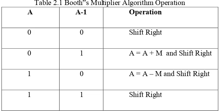
[image:21.612.151.504.526.704.2]Table 2.1 show that the Booth Multiplier Algorithm Operation, which very important for this project. The algorithm rules give a procedure for multiplying binary integers in signed –2‟s complement representation. By follow this table, to design Booth Multiplier system make easier to understand the concept [2].
Table 2.1 Booth‟s Multiplier Algorithm Operation
A A-1 Operation
0 0 Shift Right
0 1 A = A + M and Shift Right
1 0 A = A – M and Shift Right
5
2.3 Research of FPGA Implementation of Booth’s and Baugh-Wooley Multiplier Using Verilog
In the process of addition the multiple numbers of times is repeated. From the system, the number that is added is defined by multiplicand and the number of times it has to be added is given by multiplier [3]. The project of the multiplier must achieved the maximum speed in the multiplier hence, generation of partial product and adding if partial product must be optimized [3]. The multiplication perform on signed binary number and unsigned multiplication is perform on unsigned binary number is called a sign multiplication [3]. This project is to modified booth‟s algorithm in order to improve the performance which is high speed by reducing the product array multipliers [3].
Based on Figure 2.1; this is the process of booth‟s multiplier. In this block diagram, the input of multiplicand and multiplier is connecting to the control system. In multiplier the most significant bit is Xn which is the value can be added by 1 and the least significant bit is 0. The number of multiplicand must in two‟s complement or signed number. The two‟s complement happen when the value is negative. When this process is happening the value must inverted and adds to 1. Then, see the process of shifting in booth‟s bit. The process of shifting will shift to right until get the partial product. The product will save into control [4].
[image:22.612.118.540.465.690.2]Sh Ad Multiplier Cm Multiplicand two‟s Complement
Figure 2.1 Booth‟s Multiplier Block Diagram C O N T R O L
Un-1 Un-2 --- V2 V1 V0
6
2.4 FPGA Implementation of an Adaptive Hearing Aid Algorithm using Booth’s Wallace Multiplier
Hearing aids are one of many modems, portable, digital systems requiring power efficient design in order to give the life of the battery. Hearing aids are a typical example of a portable device. They include digital signal processing algorithms, which demands considerable computing power. Yet miniature pill sized batteries store to small amount of energy, limiting their lifetime [5]. Hearing impairment is often accompanied with reduced frequency selectivity which leads to a decreased speech intelligibility in noisy environments. One possibility to alleviate this efficiency is the spectral sharpening for speech enhancement based on adaptive filtering the important frequency contributions. for intelligibility in the speech are identified and accentuated [5]. This work discusses the power consumption in an FPGA implementation of the speech enhancement algorithm. It point out that power consumption can be reduce using Booth Wallace Multiplier [5].
2.4.1 Hearing Aid Architecture
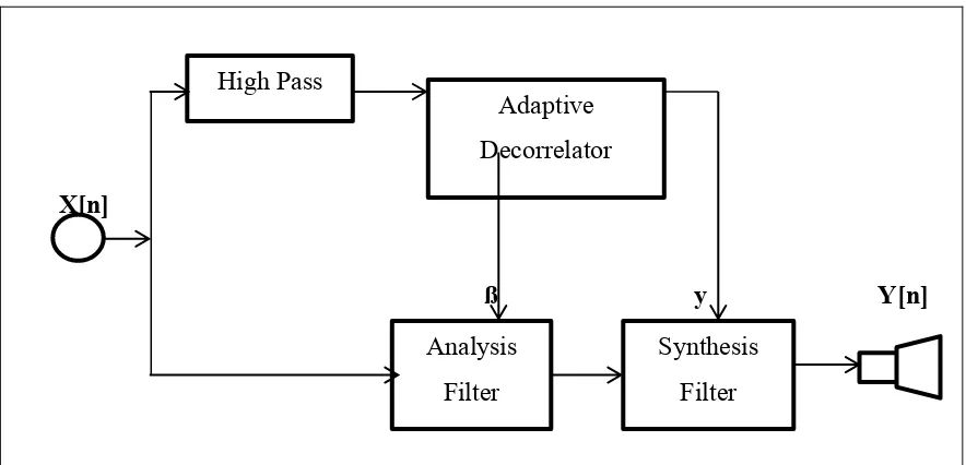
To ease the computational burden, the real-time implementation of the hearing aid utilizes a spectral sharpening and noise reduction due to spectral sharpening design for the signal processing, which is illustrated in Figure 2.2, 2.3 respectively. The input signal comes in on the upper left side of the figure, is sampled at a rate of 8 kS/s, and is delivered to the high pass filter and the filtered signal is used for updating the filter coefficients [5].
7
X[n]
[image:24.612.107.549.68.281.2]ß y Y[n]
Figure 2.2 The Spectral Sharpening Filter for Speech Enhancement
Based on the Figure 2.3, the noise reduction can be reducing by using high pass filter. The adaptive decorrelator will process by using Laplace Transform to reduce the noise from speaker. Hardware multiplication is necessary in any system that contains Digital Signal Processing (DSP) functionalities.
X[n]
ß y Y[n]
Figure 2.3 Spectral Sharpening for Noise Reduction
2.4.2 Multiplier Background
The shifts add Multiplier scheme is the most basic of unsigned integer multiplication algorithm. This algorithm uses addition and shift left operation to
High Pass
Analysis Filter
Adaptive Decorrelator
Synthesis Filter
1-A(z/ ß) 1
1 − � / ⬚
1 − −1
1 − −1
[image:24.612.110.548.432.588.2]