SYNTHESIS
Third Edition
VHDL for Logic Synthesis, Third Edition. Andrew Rushton.
SYNTHESIS
Third Edition
Registered office
John Wiley & Sons Ltd, The Atrium, Southern Gate, Chichester, West Sussex, PO19 8SQ, United Kingdom
For details of our global editorial offices, for customer services and for information about how to apply for permission to reuse the copyright material in this book please see our website at www.wiley.com.
The right of the author to be identified as the author of this work has been asserted in accordance with the Copyright, Designs and Patents Act 1988.
All rights reserved. No part of this publication may be reproduced, stored in a retrieval system, or transmitted, in any form or by any means, electronic, mechanical, photocopying, recording or otherwise, except as permitted by the UK Copyright, Designs and Patents Act 1988, without the prior permission of the publisher.
Wiley also publishes its books in a variety of electronic formats. Some content that appears in print may not be available in electronic books.
Designations used by companies to distinguish their products are often claimed as trademarks. All brand names and product names used in this book are trade names, service marks, trademarks or registered trademarks of their respective owners. The publisher is not associated with any product or vendor mentioned in this book. This publication is designed to provide accurate and authoritative information in regard to the subject matter covered. It is sold on the understanding that the publisher is not engaged in rendering professional services. If professional advice or other expert assistance is required, the services of a competent professional should be sought.
Library of Congress Cataloging-in-Publication Data Rushton, Andrew.
VHDL for logic synthesis / Andrew Rushton. – 3rd ed. p. cm.
Includes index.
Summary: ‘‘Macrocycles: Construction, Chemistry and Nanotechnology Applications is an essential introduction this important class of molecules and describes how to synthesise them, their chemistry, how they can be used as nanotechnology building blocks, and their applications’’– Provided by publisher.
ISBN 978-0-470-68847-2 (hardback)
1. VHDL (Computer hardware description language) 2. Logic design–Data processing. 3. Computer-aided design. I. Title.
TK7885.7.R87 2011 621.3905–dc22
2010045678
A catalogue record for this book is available from the British Library.
Print ISBN: 9780470688472 E-PDF ISBN: 9780470977927 O-book ISBN: 9781119995852 E-Pub ISBN: 9780470977972
Preface xi
List of Figures xv
List of Tables xvii
1 Introduction 1
1.1 The VHDL Design Cycle 1
1.2 The Origins of VHDL 2
1.3 The Standardisation Process 3
1.4 Unification of VHDL Standards 4
1.5 Portability 4
2 Register-Transfer Level Design 7
2.1 The RTL Design Stages 8
2.2 Example Circuit 8
2.3 Identify the Data Operations 10
2.4 Determine the Data Precision 12
2.5 Choose Resources to Provide 12
2.6 Allocate Operations to Resources 13
2.7 Design the Controller 14
2.8 Design the Reset Mechanism 15
2.9 VHDL Description of the RTL Design 15
2.10 Synthesis Results 16
3 Combinational Logic 19
3.1 Design Units 19
3.2 Entities and Architectures 20
3.3 Simulation Model 22
3.4 Synthesis Templates 25
3.5 Signals and Ports 27
3.6 Initial Values 29
3.7 Simple Signal Assignments 30
3.9 Selected Signal Assignment 33
3.10 Worked Example 34
4 Basic Types 37
4.1 Synthesisable Types 37
4.2 Standard Types 37
4.3 Standard Operators 38
4.4 Type Bit 39
4.5 Type Boolean 39
4.6 Integer Types 41
4.7 Enumeration Types 46
4.8 Multi-Valued Logic Types 47
4.9 Records 48
4.10 Arrays 49
4.11 Aggregates, Strings and Bit-Strings 53
4.12 Attributes 56
4.13 More on Selected Signal Assignments 60
5 Operators 63
5.1 The Standard Operators 63
5.2 Operator Precedence 64
5.3 Boolean Operators 70
5.4 Comparison Operators 73
5.5 Shifting Operators 76
5.6 Arithmetic Operators 79
5.7 Concatenation Operator 84
6 Synthesis Types 85
6.1 Synthesis Type System 85
6.2 Making the Packages Visible 87
6.3 Logic Types – Std_Logic_1164 90
6.4 Numeric Types – Numeric_Std 95
6.5 Fixed-Point Types – Fixed_Pkg 105
6.6 Floating-Point Types – Float_Pkg 119
6.7 Type Conversions 134
6.8 Constant Values 144
6.9 Mixing Types in Expressions 146
6.10 Top-Level Interface 147
7 Std_Logic_Arith 151
7.1 The Std_Logic_Arith Package 151
7.2 Contents of Std_Logic_Arith 152
7.3 Type Conversions 161
7.4 Constant Values 162
8 Sequential VHDL 167
8.1 Processes 167
8.2 Signal Assignments 170
8.3 Variables 171
8.4 If Statements 172
8.5 Case Statements 177
8.6 Latch Inference 178
8.7 Loops 181
8.8 Worked Example 187
9 Registers 191
9.1 Basic D-Type Register 191
9.2 Simulation Model 192
9.3 Synthesis Model 193
9.4 Register Templates 195
9.5 Register Types 199
9.6 Clock Types 199
9.7 Clock Gating 200
9.8 Data Gating 201
9.9 Asynchronous Reset 203
9.10 Synchronous Reset 208
9.11 Registered Variables 210
9.12 Initial Values 211
10 Hierarchy 213
10.1 The Role of Components 213
10.2 Indirect Binding 214
10.3 Direct Binding 219
10.4 Component Packages 220
10.5 Parameterised Components 222
10.6 Generate Statements 225
10.7 Worked Examples 230
11 Subprograms 243
11.1 The Role of Subprograms 243
11.2 Functions 243
11.3 Operators 254
11.4 Type Conversions 258
11.5 Procedures 261
11.6 Declaring Subprograms 267
11.7 Worked Example 270
12 Special Structures 279
12.1 Tristates 279
12.3 RAMs and Register Banks 292
12.4 Decoders and ROMs 297
13 Test Benches 301
13.1 Test Benches 301
13.2 Combinational Test Bench 302
13.3 Verifying Responses 305
13.4 Clocks and Resets 307
13.5 Other Standard Types 310
13.6 Don’t Care Outputs 312
13.7 Printing Response Values 314
13.8 Using TextIO to Read Data Files 315
13.9 Reading Standard Types 318
13.10 TextIO Error Handling 319
13.11 TextIO for Synthesis Types 321
13.12 TextIO for User-Defined Types 322
13.13 Worked Example 325
14 Libraries 327
14.1 The Library 327
14.2 Library Names 328
14.3 Library Work 329
14.4 Standard Libraries 330
14.5 Organising Your Files 333
14.6 Incremental Compilation 335
15 Case Study 337
15.1 Specification 337
15.2 System-Level Design 338
15.3 RTL Design 340
15.4 Trial Synthesis 352
15.5 Testing the Design 353
15.6 Floating-Point Version 361
15.7 Final Synthesis 362
15.8 Generic Version 364
15.9 Conclusions 366
Appendix A Package Listings 369
A.1 Package Standard 369
A.2 Package Standard_Additions 373
A.3 Package Std_Logic_1164 380
A.4 Package Std_Logic_1164_Additions 383
A.5 Package Numeric_Std 389
A.6 Package Numeric_Std_Additions 393
A.7 Package Fixed_Float_Types 400
A.9 Package Float_Pkg 415
A.10 Package TextIO 429
A.11 Package Standard_Textio_Additions 431
A.12 Package Std_Logic_Arith 432
A.13 Package Math_Real 436
Appendix B Syntax Reference 439
B.1 Keywords 439
B.2 Design Units 440
B.3 Concurrent Statements 441
B.4 Sequential Statements 443
B.5 Expressions 444
B.6 Declarations 445
References 449
The motivation for writing this book originally came from my own frustration at the lack of a synthesis-orientated book when I was learning VHDL. Not only was there a lack of information on the synthesis subset, but I found that most books on VHDL had a common problem: they described absolutely everything in an indiscriminate way, and left the reader to sort out which bits were relevant and useful. It was extremely difficult to deduce the synthesis subset from this approach.
Inthisbook, I cover the features of VHDL that you need to know for logic synthesis, from a hardware designer’s viewpoint. Each feature of the language is explained in hardware terms and the mapping from VHDL to hardware is shown. Furthermore, only the synthesisable features are presented and so there is no possibility of confusion between synthesisable and non-synthesisable features.
The exception to this rule is the chapter on test benches. Even hardware designers using the language exclusively for logic synthesis will have to write test benches and since these are not synthesised, the whole language becomes available (but not necessarily useful). So the test bench chapter introduces those parts of the language that are relevant and useful for writing test benches.
The reason that a book like this is necessary is that VHDL is a very large and clumsy language. It suffers from design-by-committee and as a result is difficult to learn, has many useless features, and I can say from my own experience, is extremely difficult to implement. I am not a champion of VHDL, but I recognise that it is still probably the best hardware description language for logic synthesis that we have. I hope that, by sharing what I have learnt of the language and how it is used for synthesis, I can help you avoid the many pitfalls that lie in wait.
I have this perspective on VHDL because I started my career as an Electronics Engineer, specialising in Digital Systems Design and gaining a BSc and PhD from the Department of Electronics at Southampton University, UK, in 1983 and 1987 respectively. However, I then moved into software engineering, but using my hardware background to develop software within the Electronics Design Automation industry. I have been working on VHDL and Electronic Design Automation using VHDL since 1988.
He took with him the key engineers for the project, and so I became one of the founder members of the new company. I was Research Manager for the new company and continued working on the logic synthesis project.
Our intention was to develop our in-house logic synthesis tool to commercial standard and sell it under the name TransGate. One of my first tasks was to help develop a VHDL front-end to the tool to replace the existing proprietary language front-end. I was very proud of the results that we achieved – TransGate had a very comprehensive support for the language, competitive with the best in the market at the time and considerably better than the majority of tools.
When we first released TransGate, we expected that engineers would take to VHDL easily, so we concentrated on the purely technical aspects of developing the synthesis algorithms. However, it gradually became apparent from feedback that users were experiencing problems with using VHDL for logic synthesis due to the learning curve associated with what was, at that time, a completely new hardware design paradigm.
As a consequence of this realisation, in 1992 I developed a new training course, offered as a public or on-site course and called ‘VHDL for Hardware Design’. This course was based on my inside knowledge of how VHDL is interpreted by a synthesiser and also on the practical problem solving that I had been involved with as part of the company’s customer support programme.
The first edition of this book, published in 1995 by McGraw-Hill, grew out of that training course. Much of the text and some of the examples were taken straight from the course. However, there is far more to a book than can be covered in a three-day long training course, so the book covered more material in far more detail than was possible in the training course. Furthermore, at the time of writing the first edition, there was an international standardisa-tion effort to define a standard set of arithmetic packages and common interpretastandardisa-tion and subset for VHDL for logic synthesis. Although this standardisation was still some way from completion at the time, nevertheless there were some aspects of logic synthesis from VHDL that had a wide consensus and this was used to inform the writing of the book.
Back at TransEDA, we were finding that the logic synthesis market niche was not only already occupied but comprehensively filled by well-established companies and we made little progress in selling our synthesis tools.
Fortunately, we branched off into code coverage tools and created a niche for ourselves in this market instead. I became the lead systems developer for the VHDLCover system. Through this project, which involved a lot of collaboration with customers, I gained experience of scores of large synthesisable VHDL designs involving hundreds of designers working in many different styles.
This change in direction of our company had a strong influence on the second edition of this book that was published in 1998 by John Wiley and Sons. Three years had passed and the standards committee had at last ratified a standard for the synthesis packages. Furthermore, exposure to many other designers’ work allowed me to take a broader view of the use of synthesis and its place in the design cycle. This made the book more user-orientated than the first edition, which did tend to dwell too much on the way that synthesisers worked. I think that the change in emphasis (slight though it was) improved the book significantly.
After TransEDA, I joined Southampton University and became a founding member of the university spin-off company Leaf-Mould Enterprises (LME). LME was formed with the intention of developing commercial behavioural synthesis systems using VHDL and based on a research programme within my old department, the Department of Electronics and Computer Science. I was responsible for the VHDL library manager, compiler and assembler which produced the concurrent assembly code from which behavioural synthesis was performed. Unfortunately, funding problems led to the demise of LME in 2001.
Since then I have become a self-employed consultant, working in a diversified range of fields: programmer, Web applications designer, systems engineer and counsellor.
It is 12 years since the publication of the second edition and it is interesting to see what has changed in the field of synthesis. The main change is that designers are moving on to system-level synthesis using C-like languages such as System Verilog, SystemC and Handel-C. However, there is clearly still a role for logic synthesis using VHDL for those who need more control over their design or, for that matter, as the synthesis engine for higher-level tools. There are now a plethora of logic synthesis tools available, for both ASIC and FPGA design.
However, VHDL itself has hardly changed at all for most of that time, with just minor tweaks to the language in 2000 and 2002. Then, in 2008, a major update was published to address a wide range of problems and to expand the range of pre-defined packages delivered with the language. Many of these changes affect synthesis. So, the time has come for a third edition of the book to reflect these changes. I have updated the whole book to reflect the current position, where the full VHDL-2008 standard is not yet available in any commercial tool, either for simulation or for synthesis, but some of the synthesis-specific features are gradually becoming available, either incorporated into the synthesis tools or as downloadable add-ons.
Figure 1.1 The VHDL-based hardware design cycle 2 Figure 2.1 Cross-product calculator – data-flow diagram 10
Figure 2.2 Adder – balanced tree 11
Figure 2.3 Adder – skewed tree 11
Figure 2.4 Cross-product calculator – datapath 14 Figure 2.5 Cross-product calculator – controller 15
Figure 3.1 Adder tree circuit 27
Figure 3.2 Hardware mapping of conditional signal assignment 31 Figure 3.3 Multi-way conditional signal assignment 32 Figure 3.4 Redundant branch in conditional signal assignment 33
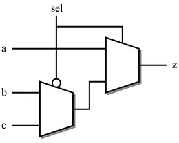
Figure 3.5 Parity generator interface 35
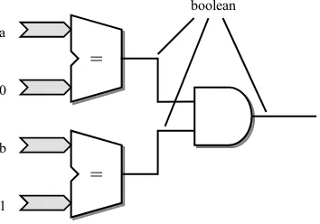
Figure 4.1 Using boolean as a comparison result 40
Figure 4.2 Intermediate value precisions 45
Figure 4.3 Multi-way selected signal assignment 61
Figure 5.1 Basic and operator 71
Figure 5.2 Selecting and operator 71
Figure 5.3 Reducing and operator 72
Figure 5.4 Four-bit equality 74
Figure 5.5 Four-bit less-than circuit 74
Figure 5.6 Array equality for arrays of equal length 75
Figure 5.7 Array less-than operator 76
Figure 5.8 Shift-left logical (sll) by 4 bits 78
Figure 5.9 Shift-left arithmetic (sla) by 4 bits 78
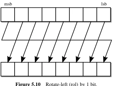
Figure 5.10 Rotate-left (rol) by 1 bit 79
Figure 5.11 Abs operator 80
Figure 5.12 Mapping of modulo-4 operator 82
Figure 5.13 Unsigned and signed modulo-4 83
Figure 5.14 Mapping of remainder operator 83
Figure 6.1 Signed resize to a larger size 97
Figure 6.2 Unsigned resize to a larger size 97
Figure 6.3 Signed resize to a smaller size 98
Figure 6.4 Unsigned resize to a smaller size 99
Figure 6.6 Floating-point storage format 120 Figure 8.1 Multiplexer interpretation of if statement 174
Figure 8.2 Multi-branch if statement 174
Figure 8.3 Incomplete if statement 177
Figure 8.4 Latch inference 180
Figure 8.5 Latched multiplexer 180
Figure 8.6 Interpretation of a for loop 184
Figure 8.7 Exit statement 186
Figure 8.8 Next statement 187
Figure 8.9 BCD to 7-segment decoder 187
Figure 8.10 Segment positions 188
Figure 8.11 Segment encodings 188
Figure 9.1 Simple combinational circuit 194
Figure 9.2 Registered circuit 194
Figure 9.3 Clock gating circuit 201
Figure 9.4 Data gating circuit 202
Figure 9.5 Asynchronous reset 204
Figure 9.6 Asynchronous reset to a value 205
Figure 9.7 Synchronous reset 209
Figure 9.8 Synchronous reset to a value 209
Figure 10.1 Target circuit 214
Figure 10.2 The two layers of indirect binding 220
Figure 10.3 For-generate circuit 227
Figure 10.4 Four-bit PRBS generator 231
Figure 10.5 Systole interface 236
Figure 10.6 Internal structure of the systole 236 Figure 10.7 Data flow of the systolic multiplier 237
Figure 10.8 Interface to the shift register 238
Figure 10.9 Internal structure of the systolic multiplier 239
Figure 12.1 Tristate driver 280
Figure 12.2 Tristate multiplexer using two drivers 283 Figure 12.3 Tristate multiplexer using one driver 284
Figure 12.4 Finite state machine 285
Figure 12.5 Signature detector state-transition diagram 285 Figure 12.6 Single-process finite state machine 289
Figure 13.1 Registered multiplexer 308
Figure 14.1 Project directory structure 334
Figure 14.2 Project subdirectory contents 335
Figure 15.1 Pass-band diagram for the low-pass filter 338
Figure 15.2 Block diagram of the FIR filter 339
Table 2.1 Scheduling and allocation for cross-product calculator 13 Table 2.2 Controller operations per clock cycle 14
Table 2.3 Comparison of synthesis results 17
Table 3.1 Event processing of adder tree 26
Table 3.2 Parity-generator functions 34
Table 4.1 Synthesisable types 38
Table 4.2 Standard types 38
Table 6.1 The synthesis type system 87
Table 6.2 Std_Logic_1164 types 91
Table 6.3 The meanings of the std_logic values 91
Table 6.4 Shift operators 101
1
Introduction
This chapter looks at the way in which VHDL is used in digital systems design, the historical reasons why VHDL was created and the international project to maintain and upgrade the language.
1.1
The VHDL Design Cycle
From its conception, VHDL was intended to support all levels of the hardware design cycle. This is clear from the preface of the Language Reference Manual (LRM) (IEEE-1076, 2008) which defines the language, from which the following quote has been taken:
VHDL is a formal notation intended for use in all phases of the creation of electronic systems. Because it is both machine readable and human readable, it supports the development, verification, synthesis, and testing of hardware designs; the communication of hardware design data; and the maintenance, modification, and procurement of hardware.
The key phrase is ‘all phases’. This means that VHDL is intended to cover every level of the design cycle from system specification to netlist. As a result, the language is rather large and cumbersome. However, this does not necessarily make it difficult to learn. It is best to think of VHDL as a hybrid language, containing features appropriate to one or more of the stages of the design cycle, so that each stage is in effect covered by a separate language that also happens to be a subset of the whole. Each subset is relatively easy to learn, provided there is guidance as to what is in, and what is not in, that subset.
In the idealised design process, there are three subsets in use – since there are three stages that use VHDL. These are: system modelling (specification phase), register-transfer level (RTL) modelling (design phase) and netlist (implementation phase).
In addition to these VHDL-based phases, there will be an initial requirements phase that is conventionally in plain (human) language. Thus, there are three stages of transformation of a design: from requirements to specification, from specification to design and from design to implementation. The first two phases are carried out by human designers, the last phase is now largely performed by synthesis.
Figure 1.1 illustrates this idealised design cycle.
VHDL for Logic Synthesis, Third Edition. Andrew Rushton.
Typically, the system model will be a VHDL model that represents the algorithm to be performed without any hardware implementation in mind. The purpose is to create a simulation model that can be used as a formal specification of the design and that can be run in a simulator to check its functionality. This specification can also be used to confirm with a customer that the requirements have been fully understood.
The system model is then transformed into a register-transfer level (RTL) design in preparation for synthesis. The transformation is aimed at a particular hardware implementation but at this stage, at a coarse-grain level. In particular, the timing is specified at the clock cycle level at this stage of the design process. Also, the particular hardware resources to be used in the implementation are specified at the block level.
The final stage of the design cycle is to synthesise the RTL design to produce a netlist, which should meet the area constraints and timing requirements of the implementation. Of course, in practice, this may not be the case, so modifications will be required which will impact on the earlier stages of the design process. However, this process is the basic, idealised, design process using VHDL and logic synthesis.
1.2
The Origins of VHDL
VHDL originated from the American Department of Defense, who recognised that they had a problem in their hardware procurement programmes. The problem was that they were receiving designs in proprietary hardware description languages, which meant that, not only was it impossible to transfer design data to other companies for second sourcing, but also there was no guarantee that these languages would survive for the life expectancy of the hardware they described.
The solution was to have a single, standard hardware description language, with a guaranteed future. Specification of such a language went ahead as part of the Very-High Speed Integrated Circuits programme (VHSIC) in the early 1980s. For this reason, the language was later named the VHSIC Hardware Description Language (VHDL).
If the language had remained merely a requirement for military procurement, it would quite possibly have remained an obscure language of interest only to DoD contractors. However, the importance of the language development, and especially the importance of standardisation of the language, was recognised by the larger electronic engineering commu-nity and so the formative language was passed into the public domain by placing it in the hands of the IEEE in 1986. The IEEE proceeded to consolidate the language into a standard that was ratified as IEEE standard number 1076 in 1987. This standard is encapsulated in the VHDL Language Reference Manual (LRM).
1.3
The Standardisation Process
Part of the standardisation process was to define a standard way of upgrading the language periodically. Thus, there is a built-in requirement for the language to be re-standardised every five years. However, in practice updates have been irregular and driven by a desire to improve the language according to demand rather than this arbitrary 5-year cycle. Because the language has changed over the years, it is sometimes important to differentiate between versions. This is done in this book by referring to the year in which the standard was ratified by the IEEE. For example, the original standard, IEEE standard number 1076, ratified in 1987, is usually referred to as VHDL-1987. Subsequent revisions of the standard will be referred to in a similar way according to their year of ratification.
Here is a summary of the different versions and the features that affect the use of the language for synthesis:
VHDL-1987 The original standard.
VHDL-1993 Added extended identifiers, xnor and shift operators, direct instantiation of components, improved I/O for writing test benches.
Most of the synthesis subset of VHDL is based on VHDL-1993. VHDL-2000 (minor revision) Nothing of relevance to synthesis.
VHDL-2002 (minor revision) Nothing of relevance to synthesis. VHDL-2008 Added fixed-point and floating-point packages.
Added generic types and packages, enabling the use of generics to define reusable packages and subprograms. Enhanced versions of conditionals. Read-ing of out ports. Improved I/O for writRead-ing test benches.
Unification of VHDL standards.
As you can see, there are only three versions of VHDL relevant to synthesis: VHDL-1987, VHDL-1993 and VHDL-2008. VHDL-1993 was the last revision to add features useful for synthesis. So VHDL-2008 is the first significant change in 15 years. A lot has been added in VHDL-2008 (Ashenden and Lewis, 2008) and most of it has some relevance to synthesis.
As a consequence, this book is based mainly on VHDL-1993. However, the more recent extensions are discussed where relevant, particularly with regard to the new fixed-point and floating-point packages added in 2008 but that have been made available as VHDL-1993 compatibility packages so that they can be used immediately on synthesisers that do not yet support the rest of VHDL-2008.
1.4
Unification of VHDL Standards
One of the largest changes in the VHDL-2008 standard is the unification of the many standards that define parts of the language and its environment.
The management of the standardisation process is down to the VHDL Analysis and Standardisation Group (VASG), part of the IEEE standardisation structure. In addition to the main standardisation process of the language itself, there are a number of working-groups working on standardisation of the ways in which VHDL is used. In the past, these working-groups have published standards of their own. For example, there was a group working on using VHDL for analogue modelling (VHDL-AMS – VHDL Analogue and Mixed-Signal – standard 1076.1), a group working on standard synthesisable numeric packages (VHDL Synthesis Package – standard 1076.3 (1997)), a group working on accelerating gate-level simulation (VITAL – the VHDL Initiative Towards ASIC Libraries – standard 1076.4), and a group working on the standard interpretation of VHDL for logic synthesis (VHDL Synthesis Interoperability – standard 1076.6). In addition, the 9-value logic typestd_logicthat is almost universally used for synthesis was developed as a completely different IEEE standard (VHDL Multivalue Logic Packages – standard 1164).
This separation of the standardisation of the various application domains of VHDL was effective in the early days of language development, because it allowed the subgroups to get on with their work independently of the main VHDL standardisation process and furthermore meant that they could publish their standards when ready, rather than waiting for the next formal release of the VHDL standard. However, this separation has become a problem as the working-groups’ work has become mature, stable and in common use. For example, a release of a new standard for VHDL could leave the subgroups’ standards lagging behind, compatible with the previous version and lacking the new language features.
So, in VHDL-2008, those working group standards that are specific to synthesis have been partlymerged into the VHDL standard itself. Standard 1076 now includes the standard logic types (1164), the standard numeric types (1076.3) and some parts of the standard synthesis interpretation (1076.6). This doesn’t make any difference to the user, but it does formalise these parts of the language as an integral part of VHDL and ensures that they stay in step with language developments in the future.
As you can probably imagine, this makes the Language Reference Manual (IEEE-1076, 2008) quite massive.
1.5
Portability
who plans for the long-term support of their designs. It is therefore good practice to write using a safe, common style of VHDL that can be expected to be supported for years to come, rather than use ‘clever’ tool-specific tricks that might not continue to be supported.
Also, it is not unusual for a company to change their preferred tools, or for a designer to be obliged to use a different synthesis tool because a different technology is being targeted. So it is good practice to write using a portable subset of synthesisable VHDL that will work across many different tools.
The problem with this principle is that synthesis relies on an interpretation of VHDL according to a set of templates, and historically each synthesis vendor has developed their own set of templates. This means that in practice, each synthesis tool supports a slightly different subset of VHDL. However, there has always been a lot of overlap between these subsets and this book attempts to identify the common denominator.
To make life more complicated, the IEEE Design Automation Standards Committee have specified a synthesis standard for VHDL (IEEE- 1076.6, 2004) that seems to be a superset rather than a subset of the VHDL supported by commercial tools. Therefore, adhering to the standard does not mean that a design will be synthesisable with any specific synthesis tool. It also seems unlikely that any single tool will implement every detail of this standard.
2
Register-Transfer Level Design
Logic synthesis works on register-transfer level (RTL) designs. What logic synthesis offers is an automated route from an RTL design to a gate-level design.
For this reason, it is important that the user of logic synthesis is familiar with RTL design to the extent that it is second nature. This chapter has been included because many designers have never used RTL designformally. This chapter serves as a simple introduction to RTL design for those readers not familiar with it. It is not meant to be a comprehensive study but it does touch on all the main issues that a designer encounters when using the method.
RTL is a medium-level design methodology that can be used for any digital system. Its use is not restricted to logic synthesis: it is equally useful for hand-crafted designs. It is an essential part of the top-down digital design process.
Register-transfer level design is a grand name for a simple concept. In RTL design, a circuit is described as a set of registers and a set of transfer functions describing the flow of data between the registers. The registers are implemented directly as flip-flops, whilst the transfer functions are implemented as blocks of combinational logic.
This division of the design into registers and transfer functions is an important part of the design process and is the main objective of the hardware designer using synthesis. The synthesis style of VHDL has a direct one-to-one relationship with the registers and transfer functions in the design.
RTL is inherently a synchronous design methodology, and this is apparent in the design of all synthesis tools.
This chapter outlines the basic steps in the RTL methodology. It is recommended that these basic steps are used when designing for logic synthesis. To illustrate the connection between RTL and logic synthesis, the examples will be written in VHDL. You are not expected to understand the full details of the VHDL at this stage, but all the VHDL used will be covered in later chapters.
VHDL for Logic Synthesis, Third Edition. Andrew Rushton.
2.1
The RTL Design Stages
The basis of RTL design is that circuits can be thought of as a set of registers and a set of transfer functions defining the datapaths between registers. The method gives a clear way of thinking about these datapaths and trying different circuit architectures while still at an abstract level. The first stage of the design is to specify at a system level (i.e.notRTL) what is to be achieved by the circuit. Typically this will be a set of arithmetic and logic operations on data coming in at the primary inputs of the circuit. At this stage there is no hardware implementation in mind; the purpose is just to create a simulation model that can then be used as the formal specification of the design. At this stage the system-level model looks more like software than hardware. The system-level model can also be used to confirm with a customer that their design requirements have been understood. Even at this early stage in the design, long before the RTL design process is complete, it is possible to write a VHDL model for simulation purposes only (not intended to be synthesisable). This is a worthwhile exercise since it tests the understanding of the problem and allows the algorithm to be checked for correctness. Later, this VHDL model can be used for comparison with the completed RTL design to verify the correctness of the design procedure. This ability to cross-check different representations of a design in the same design language using the same simulator is a powerful feature of VHDL.
The second stage of the design is to transform the system level design into an RTL design. It is rare for a design to be directly implemented in exactly the same form as the system-level model. For example, if the design performs a number of multiplications or divisions, the circuit area of the direct implementation would be excessive.
The basic design steps in using RTL are:
. identify the data operations;
. determine the type and precision of the operations; . decide what data processing resources to provide;
. allocate operations to resources;
. allocate registers for intermediate results;
. design the controller;
. design the reset mechanism.
The VHDL model of the RTL design can be simulated and checked against the system design. The third stage of the design is to synthesise the RTL design. The resulting gate-level netlist or schematic can be (and should be) simulated against the RTL design to confirm that the synthesised circuit has the same behaviour.
Finally, the netlist or schematic produced by synthesis is supplied to the placement and routing tools for circuit layout.
Needless to say, the design will probably need to go through the design/synthesise/layout cycle several times with minor or even major modifications before all the design constraints are met. Synthesis does not eliminate the need to re-iterate designs, but it does speed up the iteration time considerably.
2.2
Example Circuit
The dot product of two vectors is defined by:
ab¼X
n 1
i¼0
aibi
For the purpose of this example, to keep it simple, the size of the vectors will be fixed at 8 elements.
The system-level model in VHDL is:
package dot_product_types is
type int_vector is array (0 to 7) of integer; end;
use work.dot_product_types.all; entity dot_product is
port (a, b : in int_vector; z : out integer); end;
architecture system of dot_product is begin
process (a, b)
variable accumulator : integer; begin
accumulator := 0; for i in 0 to 7 loop
accumulator := accumulator + a(i)*b(i); end loop;
z <= accumulator; end process;
end;
This VHDL model is generally referred to as the system model. It is the simplest possible statement of the algorithm to be carried out, with no regard for data precision, timing or data storage.
In fact, since this is a very simple example, itispossible to synthesise this system model. This would not normally be the case and it should be assumed during the system modelling phase that the full range of VHDL can be used since the result is never going to be synthesised. In this example, synthesising the system model is of interest because it will give a means of comparison so that the effect of the RTL design process can be measured.
The system model was synthesised using a commercial synthesis system and targeted at a commercial ASIC library. It is not relevant which system and which library because the purpose of performing the synthesis is just to compare this direct implementation of the algorithm with the RTL model that will be developed over the rest of the chapter.
The results of synthesis were
. area – 40 000 NAND gate equivalents;
. I/O – 546 ports;
. storage – 0 registers.
reasons why this is such a large circuit is that the standard interpretation of integers is a 32-bit 2’s complement representation. This means that the multipliers and adders are all 32-bit circuits.
Clearly the direct implementation of the system model is unacceptable and a better solution should be sought. This is where RTL design comes in.
2.3
Identify the Data Operations
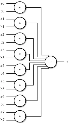
The first stage in the design process is to identify what data operations are being performed in the problem. This can be seen more clearly in the form of a data-flow diagram showing the relationship between the datapaths and the operations performed on them. This is illustrated in Figure 2.1.
It can be seen from this diagram that the dot-product calculation requires eight 2-way multiplications and one 8-way addition. These are the basic data operations required to perform the calculation.
At this stage the type of the operation should also be considered. Are the calculations acting on integers, fixed-point or floating-point types? Will a transformation be needed? For example, performing floating-point calculations is very expensive in hardware and time, so significant speed and area improvements could be made by recasting the problem onto fixed-point or even integer types.
z a0
b0 *
a1 b1 a2 b2 a3 b3 a4 b4 a5 b5 a6 b6 a7 b7
+ *
*
*
*
*
*
*
For this example, all the operations are assumed to be 2’s-complement integer arithmetic. The diagram also shows the dependencies on the data operations. The multiplications can be performed in any order or even all simultaneously since they are independent of each other. However, the additions must be carried out after the multiplications.
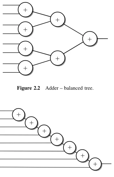
The additions have been lumped together as one operation. In practice, the additions will be performed as a series of two-way additions. They are lumped together in the figure because the ordering of the additions is irrelevant and can be chosen by the designer at a later stage in the design process so as to simplify the circuit design. This means that there are a number of structures for the data-flow diagram depending on the chosen ordering of the additions. The optimum ordering of these two-way additions will often become obvious as a design progresses. The two most likely candidates for the ordering of the additions are shown in Figures 2.2 and 2.3.
The different orderings of adders place different requirements on the ordering of the multiplications. The balanced tree for example allows an addition to be performed when any two adjacent multiplications have been performed. The multiplication pairs can be performed in any order or simultaneously. The skewed tree on the other hand places a stricter ordering on the multiplications but allows an addition after every multiplication except the first.
+
+
+
+
+
+
+
Figure 2.2 Adder – balanced tree.
+
+
+
+
+
+
+
No decision will be made at this stage of the design process, but it will become clear later in the design process that the skewed tree data-flow turns out to be the ordering for the chosen solution for this design.
Note that the two orderings of the additions illustrated here, and indeed all of the possible orderings, require seven 2-way additions.
In conclusion then, the data operations required to perform the dot-product calculation are:
. 8 multiplications;
. 7 additions.
2.4
Determine the Data Precision
In a real design, the specification would place requirements on the design, such as the expected data range, the required overflow behaviour and the maximum allowable cumulative error (for example when sampling real-world data). These factors will vary from design to design, but the key step in the design process will always be the same: to assign a precision to every data-flow such that the design meets the requirements.
This example is for illustration only, so the precision of the calculations will be chosen arbitrarily. In this case overflow during the addition will be allowed but will be ignored to keep the example simple.
In this example the following will be assumed:
. data inputs 8-bit 2’s-complement;
. all other datapaths 16-bit 2’s-complement.
2.5
Choose Resources to Provide
Having determined the data operations to be performed and the precision of those operations, it is now possible to decide what hardware resources will be provided in the circuit design to implement the algorithm.
In the simplest case, there would be a one-to-one mapping of operations onto resources. This would be a direct implementation of the algorithm in hardware. In this example, a direct implementation would require eight 8-bit multipliers (with 16-bit outputs) plus seven 16-bit adders. This is the same circuit as the system specification but with reduced precision on the datapaths.
So, in summary, the hardware resources available are:
. one, 8-bit input, 16-bit output, multiplier; . one, 16-bit input, 16-bit output, adder.
2.6
Allocate Operations to Resources
The next stage in the RTL design cycle is commonly referred to as Allocation and Scheduling. Allocation refers to the mapping of data operations onto hardware resources. Scheduling refers to the choice of clock cycle on which an operation will be performed in a multi-cycle operation. Registers must also be allocated to all values that cross over from one clock cycle to a later one. Allocation and Scheduling are interlinked and normally must be carried out simultaneously. The aim is to maximise the resource usage and simultaneously to minimise the registers required to store intermediate results.
Due to the simplicity of this example, the allocation stage is trivial since all multiplications must be allocated to the one multiplier and all the additions to the one adder.
The scheduling operation means choosing which clock cycle each multiplication and addition is to be performed. This is confused slightly by the fact that all the additions are interchangeable. Since the specification allows a multiplication and an addition in one clock cycle, the schedule can allow the product of a multiplication to be fed directly to the adder in the same clock cycle, therefore avoiding an intermediate register.
The scheduling and allocation scheme is illustrated by Table 2.1.
The whole operation of calculating the dot-product takes eight clock cycles. The algorithm has been simplified slightly by adding an eighth addition in the first cycle that effectively resets the accumulated result by adding0toproduct0instead of adding the result so far. This saves the need for a reset cycle.
Only one register is required by this scheduling since the only value that needs to be saved from one clock cycle to another is the result that is accumulated over the eight clock cycles. It is now possible to design the datapath part of the circuit minus its controller. The datapath consists of a multiplier with two inputs, one multiplexed from the set ofa0toa7, the other multiplexed from the set ofb0tob7. The product is then added to either the accumulated resultor0. Finally, the accumulatedresultis saved in a register. The circuit is shown in Figure 2.4.
Table 2.1 Scheduling and allocation for cross-product calculator
Cycle
Operator þ Operator
1 a0
b0)product0 0 þ product0)result
2 a1
b1)product1 result þ product1)result
3 a2
b2)product2 result þ product2)result
4 a3
b3)product3 result þ product3)result
5 a4
b4)product4 result þ product4)result
6 a5
b5)product5 result þ product5)result
7 a6
b6)product6 result þ product6)result
8 a7
2.7
Design the Controller
The penultimate stage in the design of the dot-product calculator is to design a controller to sequence the operations over the eight clock cycles. There are three multiplexers and a register to control in this circuit. Their operation for each of the eight clock cycles is shown in Table 2.2.
It can be seen that the multiplexers selecting between theaandbvector elements have identical operation; thezeromultiplexer selects the zero input on clock 1 and theresult input all the rest of the time; the register is permanently in load mode and so needs no control.
Normally, the controller would be implemented as a state machine. However, in this case, the state machine can be simplified to a counter that counts from 0 to 7 repeatedly. The output of the counter controls the a andb multiplexers directly. A zero detector on the counter output controls the zero multiplexer. The circuit for the controller is illustrated by Figure 2.5.
0
zero mux a mux
register
result a0
a7
b mux b0
b7
*
+
Figure 2.4 Cross-product calculator – datapath.
Table 2.2 Controller operations per clock cycle
Cycle a mux b mux Zero mux Register
1 select 0 select 0 select 0 load
2 select 1 select 1 select 1 load
3 select 2 select 2 select 1 load
4 select 3 select 3 select 1 load
5 select 4 select 4 select 1 load
6 select 5 select 5 select 1 load
7 select 6 select 6 select 1 load
2.8
Design the Reset Mechanism
The final stage of the RTL design is to design the reset mechanism. This is a simple, but essential stage of the design process. The design of a reset mechanism is an essential part of the design of the RTL system, although it is often the case that only the controller needs a reset control. If the reset mechanism is not designed into the RTL model, then there is no guarantee that the circuit will start up in a known state.
In this case, it is sufficient to reset the controller. The datapath will be cleared by the design of the controller, which resets the accumulator anyway at the start of the calculation. The controller’s reset will be incorporated as a synchronous reset.
2.9
VHDL Description of the RTL Design
Now that the RTL design process has been completed, a VHDL model can be written. This model can be simulated to verify correct behaviour by comparison with the system model that we started with. The difference is that the RTL model is clocked and needs eight clock cycles to form a result, whilst the system model was combinational and formed the result instantaneously.
library ieee;
use ieee.std_logic_1164.all, ieee.numeric_std.all; package dot_product_types is
subtype sig8 is signed (7 downto 0);
type sig8_vector is array (natural range <>) of sig8; end;
library ieee;
use ieee.std_logic_1164.all, ieee.numeric_std.all; use work.dot_product_types.all;
entity dot_product is
port (a, b : in sig8_vector(7 downto 0);
zero mux
a mux b mux
=0
ck
counter
3
ck, reset: in std_logic;
result : out signed(15 downto 0)); end;
architecture behaviour of dot_product is signal i : unsigned(2 downto 0); signal ai, bi : signed (7 downto 0);
signal product, add_in, sum, accumulator : signed(15 downto 0); begin
control: process begin
wait until rising_edge(ck); if reset = '1' then
i <= (others => '0'); else
i <= i + 1; end if; end process;
a_mux: ai <= a(to_integer(i)); b_mux: bi <= b(to_integer(i)); multiply: product <= ai * bi;
z_mux: add_in <= X"0000" when i = 0 else accumulator; add: sum <= product + add_in;
accumulate: process begin
wait until rising_edge(ck); accumulator <= sum;
end process;
output: result <= accumulator; end;
This design depends on an existing package called numeric_std that defines a set of numeric types. This will be examined in more detail in Chapter 6. For now it is sufficient to say that type unsigned represents unsigned (magnitude-only) numbers, and type signed represents signed (2’s-complement) numbers. All the VHDL used in this circuit is explained in subsequent chapters and fits the common subset of VHDL that can be synthesised by current VHDL synthesis tools.
2.10
Synthesis Results
The RTL design exercise just completed was an area constrained design. It was assumed that there would only be sufficient logic gates available to this circuit to allow a single multiplier and a single adder. It is interesting at this stage to do a comparison with the unconstrained design based on the system specification at the start of the chapter.
The RTL design was synthesised using the same synthesis system and the same target ASIC library as for the system specification.
The results of synthesis were:
. area – 1200 NAND gate equivalents; . I/O – 146 ports;
The only strange result here is the number of ports – 146 I/O pins is clearly a large overhead. However, this is simply a result of the use of an artificial example that assumes that the two vectors being used to form the dot-product are primary inputs. In practice they would probably be time-multiplexed onto either one or two input buses.
For comparison, Table 2.3 compares the synthesised RTL results with the results from synthesising the system specification. This illustrates the importance of the RTL design process.
Table 2.3 Comparison of synthesis results
System model RTL model
NAND equivalents 40 000 1200
ports 546 146
clock cycles — 8
3
Combinational Logic
This chapter will describe the basics of VHDL required to describe combinational logic using basic types to create boolean equations and simple arithmetic circuits.
It will also introduce the simulation model of VHDL, with an introduction to modelling concurrency, how this is done using the event model and the concepts of simulation time and delta time.
This chapter will then show how this model is used by synthesis tools to control the mapping of VHDL descriptions to circuits, and introduces synthesis templates.
3.1
Design Units
Design Units are the basic building blocks of VHDL. They are indivisible in that a design unit must be completely contained in a single file. A file may contain any number of design units.
When a file is analysed using a VHDL simulator or synthesiser, the file is, in effect, broken up into its individual design units and each design unit is analysed separately as if they had been in separate files.
There are six kinds of design units in VHDL. These are:
. entity;
- architecture; . package;
- package body;
. configuration declaration;
. context declaration.
The six kinds of design unit are further classified as primary or secondary units. A primary design unit can exist on its own. A secondary design unit cannot exist without its corresponding primary unit. In other words, it is not possible to analyse a secondary unit before its primary unit is analysed. The secondary units are shown above indented and immediately below their corresponding primary units.
VHDL for Logic Synthesis, Third Edition. Andrew Rushton.
The entity is a primary design unit that defines the interface to a circuit. Its corresponding secondary unit is the architecture that defines the contents of the circuit. There can be many architectures associated with a particular entity, but this feature is rarely, if ever, used in synthesis and so will not be covered here.
The package is also a primary design unit. A package declares types, subprograms, operations, components and other objects that can then be used in the description of a circuit. The package body is the corresponding secondary design unit that contains the implementations of subprograms and operations declared in its package. This will not be covered yet, but the usage of packages supplied with the synthesiser is covered throughout the book and how to declare your own is covered in Chapters 10 and 11.
The configuration declaration is a primary design unit with no corresponding secondary. It is used to define the way in which a hierarchical design is to be built from a range of subcomponents. However, it is not generally used for logic synthesis and will not be covered in this book.
The context declaration is a new primary unit with no corresponding secondary, and was added in VHDL-2008. It allows multiple context clauses (i.e.libraryanduseclauses) to be grouped together. However, because it is not in common use it will not be used in this book, except in Chapter 6 where other VHDL-2008 features are discussed.
3.2
Entities and Architectures
An entity defines the interface to a circuit and the name of the circuit. An architecture defines the contents of the circuit itself. Entities and architectures therefore exist in pairs – a complete circuit description will generally have both an entity and an architecture. It is possible to have an entity without an architecture, but such examples are generally trivial and of no real use. Also, it is possible to have multiple architectures for a single entity, each one representing a different implementation of the same circuit. This can be useful when comparing different levels of model, such as comparing the RTL model with the gate-level model. It is not possible to have an architecture without an entity.
An example of an entity is:
entity adder_tree is
port (a, b, c, d : in integer; sum : out integer); end entity adder_tree;
In this case, the circuitadder_treehas five ports: four input ports and one output port.
Note that the repeat of the keywordentity and the circuit nameadder_treeafter the
endare both optional and in practice are usually omitted.
The structure of an architecture is illustrated by the following example:
architecture behaviour of adder_tree is signal sum1, sum2 : integer;
begin
The architecture has the namebehaviourand belongs to the entityadder_tree. It is common practice to use the architecture namebehaviourfor all synthesisable architectures. As with the entity, the repeat of thearchitecturekeyword and namebehaviourafter the
end is optional and usually omitted. Common alternatives to architecture behaviour
are architecture RTLor architecture synthesis. Architecture names do not need to be
unique, indeed the consistent use of the same architecture name throughout a VHDL design is considered best-practice because it makes it easy to tell at a glance whether a VHDL
description is system level (architecture system), RTL (architecture behaviour) or
gate-level (architecturenetlist). It does not matter what naming convention is used for architectures but it is recommended that a consistent naming convention is adhered to.
The architecture has two parts.
The declarative part is the part before the keywordbegin. In this example, additional internal signals have been declared here. Signals are similar to ports but are internal to the circuit.
A signal declaration looks like:
signal sum1, sum2 : integer;
This declares two signals calledsum1andsum2that have a type calledinteger. Basic types will be dealt with in Chapter 4, and a set of synthesis-specific types are covered in Chapter 6, so for now it is sufficient to say that integer is a numeric type that can be used for calculations.
The statement part is the part after thebegin. This is the description of the circuit itself. In this example the statement part only contains signal assignments describing the adder tree as three adders described by equations.
The simple signal assignment looks like:
sum1 <= a + b;
The left-hand side of the assignment is known as the target of the assignment (in this case sum1). The assignment itself has the symbol"<¼"that is usually read ‘gets’, as in ‘signal sum1 gets a plus b’.
The right-hand side of the assignment is known as the source of the assignment. The source
expression can be as complex as you like. For example, the circuit of the adder_tree
example could have been written using just one signal assignment:
sum <= (a + b) + (c + d);
The example was written with three assignments so that the relationship between assignments, ports and signal declarations could be explained.
architecture behaviour of adder_tree is signal sum1, sum2 : integer;
begin
sum <= sum1 + sum2; sum2 <= c + d; sum1 <= a + b; end;
3.3
Simulation Model
In order to really understand how VHDL works, it is useful to have a basic knowledge of the underlying mechanisms of the language. This will help to explain many VHDL features introduced in this and subsequent chapters.
VHDL has been designed from the start as a simulation language, so an understanding of the language must come from examining the behaviour of a VHDL simulator. The definition of VHDL contained in the Language Reference Manual includes a definition of how a simulator should implement the language, so this behaviour must be common to all VHDL simulators. The basis of VHDL simulation is event processing. All VHDL simulators are event-driven simulators.
There are three essential concepts to event-driven simulation. These are: simulation time, delta time and event processing.
During a simulation, the simulator keeps track of the current time that has been simulated, that is, the circuit time that has beenmodelledby the simulator, not the time the simulation has actually taken. This time is known as thesimulation timeand is usually measured as an integral multiple of a basic unit of time known as the resolution limit. The simulator cannot measure time delays less than the resolution limit. For gate-level simulations the resolution limit may be quite fine, possibly 1 fs or less. For RTL simulations, there is no need to specify a fine resolution since we are only interested in clock-cycle by clock-cycle behaviour and the transfer functions are described with zero or unit time delay. In this case, a resolution limit of 1 ps is often used. It is important to note that the resolution limit is a characteristic of the simulator, not of the VHDL model. It is usually controlled by a simulator configuration setting.
The simulation cycle alternates betweenevent processingandprocess execution. Put another way, signals are updated as a batch in the event processing part of the cycle, then processes are run as a batch in the process execution part. The signal updating and process execution are kept completely separate. This is how VHDL models concurrency such that it can be modelled on a sequential computer processor without having to use multiple processors or threads.
When a signal assignment (a simplified process) is performed, the signal that is the target of the assignment is not updated immediately by the assignment; in fact it keeps its old value for the remainder of the process execution phase. Instead, the assignment causes atransactionto be added to a queue of transactions associated with thedriverof the signal.
For example:
a <= '0' after 1 ns, '1' after 2 ns;
a <= '0';
This contains one transaction with the value of'0'and no time delay. Even when there is no time delay the signal is not updated immediately, since the transaction will be scheduled for the nextdelta cycle.
When simulation time moves on to the point where a transaction becomes due on a signal, then during the event-processing phase that signal becomes active. The new value is then compared with the old value and, if the value has changed, then aneventis generated for that signal. This event causes processes sensitive to the signal to be triggered. Note that, if the signal is assigned a value that is the same as its current value, it will become active but will not have an event and so will not trigger any processes.
An event is processed by updating the signal value, then working out which statements have that signal as an input (in VHDL-speak, all the statements that aresensitiveto that signal). All signals are processed as a batch, that is, all signals that have an event in the current simulation cycle are updated in this way. The set of processes triggered by these signal updates are scheduled for execution during a later process execution phase. Each process can only be triggered once per simulation cycle, no matter how many of its inputs change.
During the process execution phase, each process is executed until it pauses. The simulator works its way through all the triggered processes in no particular order executing them until they pause. Only after all the triggered processes have paused will the simulator switch back to the event-processing phase.
Any signal assignments in the executed processes cause more transactions to be generated. These new transactions are processed in later simulation cycles. Zero-delay assignments will be processed in the next delta cycle.
The distinction between an active signal and a signal event is very important. Processes are sensitive to events, so will only be activated by a signal changing its value. This is generally what is wanted. For example, consider the following RS latch model:
P1: process (R, Qbar) begin
Q <= R nor Qbar; end process;
P2: process (S, Q) begin
Qbar <= S nor Q; end process;
This example has been written using processes to show the sensitivity list. This is the list of signals in parentheses after the keywordprocess, which represents the set of signals that will
triggerthe process. For combinational logic, the sensitivity list should include all of the inputs of the process, in this case all of the signals on the source (right-hand) side of the signal assignments.
The example could have been written without processes, using just simple signal assignments:
This is exactly equivalent since the VHDL standard states that a signal assignment has an implied sensitivity list containing all the signals on its right-hand side. In other words, assignmentP1will trigger on changes toRorQbar, whilst assignmentP2will trigger on changes toSorQ.
Consider the case whenRandSare'0', withQat'1'andQbarat'0'. Consider what then happens whenRchanges due to a transaction of value'1'at the current simulation time. The model will go through the following sequence:
delta 1, event processing
The transaction makesRactive and, since it is a change in value forR(from'0'to'1'), it causes an event onR. The event onRtriggers processP1that is sensitive to it.
delta 1, process execution
P1recalculates the value ofQ, creating a transaction of value'0'(since'1' nor '0'is '0') at the current time. This transaction is added to the transaction queue forQ. delta 2, event processing
The transaction onQmakesQactive and, since it is a change in value forQ(from'1'to '0'), it causes an event onQ. The event onQtriggers processP2that is sensitive to it. delta 2, process execution
P2recalculates the value ofQbar, creating a transaction of value'1'(since'0' nor '0' is'1') at the current time. This transaction is added to the transaction queue forQbar. delta 3, event processing
The transaction onQbarmakesQbaractive and, since it is a change in value forQbar (from'0'to'1'), it causes an event onQbar. The event onQbartriggers processP1for the second time.
delta 3, process execution
P1recalculates the value ofQ, creating a transaction of value'0'(since'1' nor '1'is '0') at the current time. This transaction is added to the transaction queue forQ. delta 4, event processing
The transaction onQmakesQactive but, since it is not a change in value forQ(from'0'to '0'), it does not cause an event onQ.
Since there are no more transactions to process in the model, the model reaches a stable state at this point. The simulation time can now be moved on to the next scheduled transaction onRorS and a similar series of delta cycles will be carried out.
The important thing about the way VHDL models the circuit is that the signal/process delta cycles stopped because a transaction did not result in a change in a signal, so no events were generated, even though a signal did become active in the last cycle. As you can see from this example, this means that VHDL models asynchronous feedback simply and naturally. It also means that the order in which the processes or signal assignments are listed in the architecture has no effect on the simulation, since the decisions determining which processes to execute are based purely on the events and process sensitivity lists, not on the order of the statements. Swapping the two processes would result in exactly the same sequence. VHDL is aconcurrent
language.
To further illustrate the action of an event-driven simulator to show how values
propagate through a circuit, consider the behaviour of the adder_tree example
intro-duced earlier.
For this example, it will be assumed that the circuit is initially in a stable state with all the inputs set to0. It can be seen from the description of the adder tree that all the internal signals and the outputs will also be0. These values are set up during the initialisation (or elaboration) phase of simulation, which happens at time zero.
Consider what happens if the inputbchanges from0to1at a simulation time of 20 ns. This means that a transaction is generated for signalband this transaction is posted at the first delta cycle of the 20 ns simulation time. When this transaction is processed, it is tested to see if it is a change in value, which it is, so this causes an event onb. The event processing causes the equations that are sensitive tobto be triggered. These are:
sum1 <= a + b;
So this equation is executed during the process execution phase. As a result of recalculating this equation, a transaction is generated forsum1at the current simulation time (20 ns), but at the next delta cycle. At this stage, signalsum1has not changed value; the only outcome of the process execution is that a transaction is posted forsum1specifying a new value of1(i.e.
0þ1)for signalsum1.
The next stage of the simulation is transaction processing of the second delta cycle. First, the transaction on signalsum1 is tested to see if it changes its value, which it does, so the transaction is transformed into an event.
Then, all equations sensitive tosum1are triggered. The sensitive equations are:
sum <= sum1 + sum2;
Process execution is carried out on this equation, generating transactions for the next delta cycle. One new transaction is generated in this case and posted at the third delta cycle at the current simulation time. The transaction is a new value forsum2of1. Once again, this value is not yet assigned to the signal.
Transaction processing of the third delta cycle causes the transaction onsumto be tested to see if it represents a change of value. Once again it is a change, so the transaction is transformed into an event, triggering equations sensitive to it. No equations are sensitive to the output signals, so there are no further transactions to process and simulation of the current simulation time has now completed. Simulation time can now be moved on.
The whole simulation cycle is summarised in Table 3.1.
Note how the change on the input propagated through to thesumoutput over three delta cycles. The result is that a minimum set of processes was re-executed as a result of the input change and that some processes were not re-executed at all.
3.4
Synthesis Templates
language. This interpretation is based on mappings of special VHDL constructs onto hardware with equivalent behaviour.
These special constructs are known astemplates.
The mapping is not always straightforward. Some VHDL constructs have direct one-to-one mappings to hardware equivalents. Many VHDL constructs have no possible hardware equivalents, at least within the confines of logic synthesis, and these will cause errors during synthesis. Other constructs have to meet specific constraints in order to be mappable. Synthesisers must impose these constraints on the use of the language so that only VHDL constructs that have hardware equivalents can be used. In other words, your VHDL must conform to the appropriate template for the hardware structure you wish to build.
There are templates for combinational logic, simple registers, registers with asynchronous reset, registers with synchronous reset, latches, RAMs, ROMs, tristate drivers and finite-state machines, all of which will be covered later in this book.
Note:you might come across the synthesis subset of VHDL expressed as a restrictedsyntax. This is unhelpful since the synthesis subset is really asemanticsubset. That is, most VHDL constructs are synthesisable provided that they are used in a particular, constrained way that fits one of the synthesis templates.
It is extremely important to conform to these templates since they dictate how VHDL must be written in order to be synthesisable. VHDL models must be written for synthesis from the start; it is not possible to take just any VHDL that simulates correctly and expect it to be synthesisable. Many person-years of work have been wasted by engineers who failed to realise this and wasted their time perfecting simulation models before considering the synthesis constraints.
Fortunately, in the case of the adder_tree example, the circuit interpretation is a simple and direct mapping to hardware. VHDL signal assignments map directly onto blocks of combinational logic. This can be seen by considering the event processing cycle described earlier. At each stage, every equation that is sensitive to a changing input is recalculated. This is the behaviour of combinational logic in which the output is re-evaluated whenever an input changes. The expressions used (þ operators) have direct equivalents in hardware too. These equivalences together give us the mapping from simulation behaviour to circuit structure.
In later chapters, similar parallels will be drawn to show how the simulation model of other constructs can be mimicked by certain hardware structures. It is this mimicry that gives us the Table 3.1 Event processing of adder tree
20 ns 20 nsþd 20 nsþ2d 20 nsþ3d
a 0 0 0 0
b 0 1 1 1
c 0 0 0 0
d 0 0 0 0
sum1 0 0 1 1
sum2 0 0 0 0
sum 0 0 0 1
transactions b)1 sum1)1 sum)1
hardware mapping. It should always be remembered that VHDL is a simulation language and that not all simulation constructs have hardware equivalents. This is why all synthesisers must work on subsets of the language.
Figure 3.1 illustrates the circuit representation of theadder_treeentity/architecture pair. In this figure, the operations have been represented by simple circles rather than as gates to highlight the fact that, at this stage, there has been no mapping to gates. Instead the circuit has been shown as a network of abstract arithmetic functions. A synthesiser