Power Electronic
Converters
Power Electronic
Converters
Interactive Modelling Using Simulink
By
not constitute endorsement or sponsorship by The MathWorks of a particular pedagogical approach or particular use of the MATLAB® and Simulink® software.
CRC Press
Taylor & Francis Group
6000 Broken Sound Parkway NW, Suite 300 Boca Raton, FL 33487-2742
© 2018 by Taylor & Francis Group, LLC
CRC Press is an imprint of Taylor & Francis Group, an Informa business
No claim to original U.S. Government works Printed on acid-free paper
International Standard Book Number-13: 978-0-8153-6819-9 (Hardback)
This book contains information obtained from authentic and highly regarded sources. Reasonable efforts have been made to publish reliable data and information, but the author and publisher cannot assume responsibility for the validity of all materials or the conse-quences of their use. The authors and publishers have attempted to trace the copyright holders of all material reproduced in this publication and apologize to copyright holders if permission to publish in this form has not been obtained. If any copyright material has not been acknowl-edged please write and let us know so we may rectify in any future reprint.
Except as permitted under U.S. Copyright Law, no part of this book may be reprinted, repro-duced, transmitted, or utilized in any form by any electronic, mechanical, or other means, now known or hereafter invented, including photocopying, microfilming, and recording, or in any information storage or retrieval system, without written permission from the publishers.
For permission to photocopy or use material electronically from this work, please access www. copyright.com (http://www.copyright.com/) or contact the Copyright Clearance Center, Inc. (CCC), 222 Rosewood Drive, Danvers, MA 01923, 978-750-8400. CCC is a not-for-profit orga-nization that provides licenses and registration for a variety of users. For orgaorga-nizations that have been granted a photocopy license by the CCC, a separate system of payment has been arranged.
Trademark Notice: Product or corporate names may be trademarks or registered trademarks, and are used only for identification and explanation without intent to infringe.
Visit the Taylor & Francis Web site at http://www.taylorandfrancis.com
Dedicated to the memory of the late Dr. Venkat Ramaswamy,
vii
Contents
Preface ... xiii
1 Introduction ...1
1.1 Background ...1
1.2 Why Use Simulink? ...2
1.3 Significance of Modelling ...2
1.4 Book Novelty ...3
1.5 Book Outline ...4
References ...5
2 Fundamentals of Interactive Modelling ...7
2.1 Introduction ...7
2.2 Interactive Modelling Concept ...7
2.3 Interactive Modelling Procedure ...8
2.3.1 Interactive Model Development ...9
2.3.2 Three-Phase AC Voltage Source ... 12
2.3.3 SCR Three-Phase Half-Wave Converter ... 16
2.3.4 Gate Pulse Generator ... 18
2.3.5 RLE Load ... 21
2.3.6 Output Voltage and Current Measurement ... 21
2.3.7 Input Voltage Measurement ... 24
2.4 Simulation Results ... 27
2.5 Discussion of Results ... 28
2.6 Conclusions ... 28
References ... 29
3 Interactive Models for AC to DC Converters ... 31
3.1 Introduction ... 31
3.2 Single-Phase Full-Wave Diode Bridge Rectifier ... 31
3.2.1 Interactive Model for Single-Phase FWDBR with Purely Resistive or with RLE Load ... 32
3.2.2 Simulation Results ... 36
3.3 Single-Phase Full-Wave SCR Bridge Rectifier ... 38
3.3.1 Model for Single-Phase FWCBR with Purely Resistive or with RLE Load ... 39
3.3.2 Simulation Results ...44
3.4 Three-Phase Full-Wave Diode Bridge Rectifier ... 46
3.4.1 Model for Three-Phase FWDBR with Purely Resistive Load ...48
3.5 Conclusions ... 56
References ... 56
4 Interactive Models for DC to AC Converters ... 57
4.1 Introduction ... 57
4.2 Three-Phase 180° Mode Inverter ... 57
4.2.1 Analysis of Line-to-Line Voltage ... 58
4.2.2 Analysis of Line-to-Neutral Voltage ... 60
4.2.3 Total Harmonic Distortion ...63
4.2.4 Model for Three-Phase 180° Mode Inverter ...63
4.2.5 Simulation Results ... 67
4.3 Three-Phase 120° Mode Inverter ... 68
4.3.1 Analysis of Line-to-Line Voltage ... 71
4.3.2 Analysis of Line-to-Neutral Voltage ... 73
4.3.3 Total Harmonic Distortion ... 75
4.3.4 Model of Three-Phase 120° Mode Inverter ... 76
4.3.5 Simulation Results ... 78
4.4 Three-Phase Sine PWM Technique ...80
4.4.1 Model for Three-Phase Sine PWM Inverter ...84
4.4.2 Simulation Results ... 86
4.5 Conclusions ... 87
References ...90
5 Interactive Models for DC to DC Converters ... 91
5.1 Introduction ... 91
5.2 Buck Converter Analysis in Continuous Conduction Mode ... 91
5.3 Buck Converter Analysis in Discontinuous Conduction Mode ... 94
5.4 Model of Buck Converter in CCM and DCM ... 95
5.4.1 Simulation Results ... 97
5.5 Boost Converter Analysis in Continuous Conduction Mode ... 101
5.6 Boost Converter Analysis in Discontinuous Conduction Mode ....103
5.7 Model of Boost Converter in CCM and DCM ... 105
5.7.1 Simulation Results ... 106
5.8 Buck–Boost Converter Analysis in Continuous Conduction Mode ...106
5.9 Buck–Boost Converter Analysis in the Discontinuous Conduction Mode... 112
5.10 Model of Buck–Boost Converter in CCM and DCM ... 114
5.10.1 Simulation Results ... 115
5.11 Conclusions ... 115
References ... 120
6 Interactive Models for AC to AC Converters ... 121
6.1 Introduction ... 121
ix
Contents
6.2.1 Modelling of a Fully Controlled Phase Three-Wire AC Voltage Controller with Star-Connected
Resistive Load and Isolated Neutral ...124
6.2.2 Simulation Results ... 129
6.3 Analysis of a Fully Controlled Three-Phase AC Voltage Controller in Series with Resistive Load Connected in Delta ... 133
6.3.1 Modelling of a Fully Controlled Three-Phase AC Voltage Controller in Series with Resistive Load Connected in Delta ... 135
6.3.2 Simulation Results ... 140
6.4 Conclusions ... 144
References ... 145
7 Interactive Modelling of a Switched Mode Power Supply Using Buck Converter ... 147
7.1 Introduction ... 147
7.2 Principle of Operation of Switched Mode Power Supply ... 147
7.3 Modelling of the Switched Mode Power Supply ... 150
7.3.1 Simulation Results ... 153
7.4 Conclusions ... 155
References ... 163
8 Interactive Models for Fourth-Order DC to DC Converters ... 165
8.1 Introduction ... 165
8.2 Analysis of SEPIC Converter in CCM ... 165
8.3 Analysis of SEPIC Converter in DCM ... 168
8.4 Model of SEPIC Converter in CCM and DCM ... 171
8.4.1 Simulation Results ... 174
8.5 Analysis of Quadratic Boost Converter in the CCM ... 176
8.6 Analysis of Quadratic Boost Converter in the DCM ... 181
8.7 Model of Quadratic Boost Converter in CCM and DCM ... 184
8.7.1 Simulation Results ... 191
8.8 Analysis of Ultra-Lift Luo Converter in the CCM ... 191
8.9 Analysis of Ultra-Lift Luo Converter in DCM ... 194
8.10 Model of Ultra-Lift Luo Converter in CCM and DCM ... 197
8.10.1 Simulation Results ... 200
8.11 Conclusions ... 202
References ... 205
9 Interactive Models for Three-Phase Multilevel Inverters ... 207
9.1 Introduction ... 207
9.2 Three-Phase Diode-Clamped Three-Level Inverter ... 208
9.2.1 Modelling of Three-Phase Diode-Clamped Three-Level Inverter ... 209
9.3 Three-Phase Flying-Capacitor Three-Level Inverter ... 214
9.3.1 Modelling of Three-Phase Flying-Capacitor Three-Level Inverter ... 218
9.3.2 Simulation Results ... 221
9.4 Three-Phase Cascaded H-Bridge Inverter ... 221
9.4.1 Modelling of Three-Phase Five-Level Cascaded H-Bridge Inverter ...225
9.4.2 Simulation Results ... 232
9.5 RMS Value and Harmonic Analysis of the Line-to-Line Voltage of Three-Phase DCTLI and FCTLI ... 235
9.6 RMS Value and THD of Phase-to-Ground Voltage of TPFLCHB Inverter ... 237
9.7 Pulse Width Modulation Methods for Multilevel Converters.... 238
9.7.1 Multi-Carrier Sine Phase-Shift PWM ... 239
9.7.2 Simulation Results ... 243
9.7.3 Multi-Carrier Sine Level Shift PWM... 243
9.7.4 Simulation Results ... 249
9.8 Conclusions ... 249
References ... 251
10 Interactive Model Verification ... 253
10.1 Introduction ... 253
10.2 AC to DC Converters ... 253
10.2.1 Single-Phase Full-Wave Diode Bridge Rectifier ... 253
10.2.2 Single-Phase Full-Wave SCR Bridge...254
10.2.3 Three-Phase Full-Wave Diode Bridge Rectifier ...254
10.3 DC to AC Converters ... 256
10.3.1 Three-Phase 180° Mode Inverter ... 258
10.3.2 Three-Phase 120° Mode Inverter ... 258
10.4 DC to DC Converter ... 260
10.4.1 Buck Converter ... 260
10.4.2 Boost Converter ... 262
10.4.3 Buck–Boost Converter ... 265
10.5 AC to AC Converter ... 265
10.5.1 Three-Phase Thyristor AC to AC Controller Connected to Resistive Load in Star ... 267
10.5.2 Three-Phase Thyristor AC to AC Controller in Series with Resistive Load in Delta ... 270
10.6 Switched Mode Power Supply Using Buck Converter... 272
10.7 Fourth-Order DC to DC Converters... 280
10.7.1 SEPIC Converter ... 282
10.7.2 Quadratic Boost Converter ... 283
xi
Contents
10.8 Three-Phase Three-Level Inverters ... 290
10.8.1 Three-Phase Diode-Clamped Three-Level Inverter ... 292
10.8.2 Three-Phase Flying-Capacitor Three-Level Inverter ... 292
10.9 Three-Phase Sine PWM Inverter ... 297
10.10 Three-Phase Five-Level Cascaded H-Bridge Inverter ...300
10.11 Pulse Width Modulation Methods for Multilevel Converters.... 310
10.11.1 Multi-Carrier Sine Phase-Shift PWM ... 310
10.11.2 Multi-Carrier Sine Level Shift PWM... 315
10.12 Conclusions ... 318
References ... 319
11 Interactive Model for and Real-Time Simulation of a Single-Phase Half H-Bridge Sine PWM Inverter ... 321
11.1 Introduction ... 321
11.2 Interactive Model of Single-Phase Half H-Bridge Sine PWM Inverter ... 322
11.2.1 Simulation Results ... 322
11.3 Real-Time Software in the Loop Simulation ... 322
11.3.1 Digital Signal Processor ... 322
11.3.2 Code Composer Studio ... 324
11.3.3 Symmetric PWM Waveform Generation ... 324
11.3.4 Sine-Triangle Carrier PWM Generation ... 328
11.4 Conclusions ... 332
References ... 333
xiii
Preface
This textbook provides a step-by-step method for the development of a virtual interactive power electronics laboratory. Therefore, this textbook is suitable for undergraduates and graduates in electrical and electronics engineering for their laboratory courses and projects in power electronics. This textbook is equally suitable for practising professional engineers in the power electronics industry. They can develop an interactive virtual power electronics laboratory as outlined in this textbook and perform simulation of their new power electronic converter designs. Similarly, instructors may find this textbook useful for running an interactive virtual laboratory course or a new project in the area of power electronics.
The topic of power electronic converter modelling is a growing field. There are many software packages available for this purpose. Most of them are power electronic circuit simulation packages using semiconductor and other passive components. Circuit component-level simulation of power electronic converters is a basic or fundamental level of modelling. A higher level of modelling is the system model, which solves the characteristic equations describing the behaviour of the power electronic converter. The Simulink® software, developed by The Mathworks Inc., USA, can be used to develop advanced system models as well as circuit component-level models for any given power electronic converter. Moreover, it is possible to develop both interactive system models and circuit component-level models using Simulink, which is a special feature. Therefore, I have used Simulink to develop interactive models of power electronic converters presented in this textbook. Unless specified otherwise, the term model in this textbook refers to Simulink model.
Chapter 1 provides the introduction, where the significance of modelling power electronic converters, the novelty of this textbook and the reason for the choice of the Simulink software are presented. The fundamentals of developing interactive models are presented in Chapter 2 with an example of a three-phase half-wave thyristor rectifier converter. This chapter also highlights the advantage of interactive modelling, which is primarily the saving in time in testing power electronic converters by model simulation. Interactive system models of power electronic converters are presented in the following order:
To verify the performance of the system models of the power electronic converters in Chapters 3 to 9, Chapter 10 has been added. Chapter 10 pro-vides the interactive component-level models of the power electronic con-verters presented in Chapters 3 to 9.
An interactive component-level model and real-time software in the loop (SIL), also known as processor in the loop (PIL) simulation of a single-phase half H-bridge sine pulse width modulation (PWM) inverter is presented in Chapter 11. This work was carried out by the author while a research fellow in the Faculty of Engineering, University of Nottingham, UK. The author is grateful to Prof. Alberto Castellazzi and Prof. Pat Wheeler, both of the School of Electrical and Electronics Engineering, University of Nottingham, UK, for their support in carrying out this work.
As mentioned before, it is possible to develop system models of power electronic converters using the Simulink block set and circuit component-level models using the Simscape-Electrical, Power Systems and Specialized Technology block sets.
Much of the material presented in this textbook is work undertaken by the author during his Master of Engineering degree by research programme at the University of Technology Sydney, NSW, Australia. The author is grate-ful to the late Dr. Venkat Ramaswamy, formerly senior lecturer, School of Electrical Engineering, University of Technology Sydney, NSW, who was a great source of encouragement and support. The author also wishes to thank Dr. Jianguo Zhu, head, School of Electrical Engineering, University of Technology Sydney, NSW, for his support.
The whole of Chapter 8 and the models in Sections 5.4, 5.7 and 5.10 and in Sections 9.4 and 9.7 are my original contributions and are not a part of the above research work.
No end of chapter exercises are given, as this seems to be unnecessary. The reader can practice interactive modelling according to the method outlined here in this book and using the many textbooks on power electronics, some of which are mentioned in the references at the end of each chapter.
The step-by-step interactive modelling details are explained in Chapter 2 only. They are not repeated in Chapters 3 to 11, as most of the sources and components used in the power electronic converter shown in Chapter 2 are repeatedly used in the converters presented in these chapters.
The whole of Chapter 10, excluding Sections 10.7, 10.8, 10.10 and 10.11, is suitable for a senior-level undergraduate curriculum in power electronics.
The model files in this textbook can be found on the website https://www. crcpress.com/Power-Electronic-Converters-Interactive-Modelling-Using-Simulink/Iyer/p/book/9780815368199. Instructors can download a copy of these model files.
xv
Preface
I would like to thank Ms. Nora Konopka, Editorial Director: Engineering, CRC Press for her help and support. Also, many thanks to the anonymous reviewers for their valuable comments.
Finally, I would like to thank my wife, Mythili Iyer, for her patience and understanding. Without her support, this work would not have been possible.
Narayanaswamy P. R. Iyer
Sydney, NSW Australia
MATLAB® is a registered trademark of The MathWorks, Inc. For product information, please contact:
The MathWorks, Inc. 3 Apple Hill Drive
Natick, MA 01760-2098 USA Tel: 508 647 7000
Fax: 508-647-7001
1
1
Introduction
1.1 Background
The performance of power electronic converters can be studied using mathematical equations which describe the behaviour of the particular converter. For example, the load current and load voltage pattern for a single-phase full-wave diode bridge rectifier delivering power to a series-connected R–L load can be studied by developing and then solving the differential equation describing the behaviour of this converter. The power electronic converter supplying power to these loads can be developed either as a system model that duplicates the performance of this converter or as a circuit model using the actual power electronic semiconductor and other passive components.
1.2 Why Use Simulink?
In this book, I have used Simulink® software developed by The Mathworks Inc. [10]. Simulink has the following advantages compared with other soft-ware packages with regard to power electronic circuit simulation:
• Facility to develop interactive models with user dialogue boxes for power electronic systems, with which any given power electronic converter can be tested by entering the parameters in the dialogue boxes without actually going into each block of the model to enter the data. This saves time for the user and finds applications in the virtual power electronics laboratory. This is one of the unique fea-tures in Simulink.
• Harmonic analysis of power electronic converters can be easily developed with Powergui in the PowerSystems block set.
• Many non-linear phenomena such as pulse width modulation (PWM) techniques can be easily verified.
• Many power electronic circuits can be studied by modelling tech-niques and can be verified by semiconductor components in the PowerSystems block set; that is, it is possible to develop both system models based on the characteristic equations describing the behav-iour of the system and electronic circuit component-level models utilising the equivalent circuit parameters of the semiconductor component.
• Facility to study analogue and digital gate drives used in power electronic circuits.
• Facility to save data in workspace, which can be later brought to the MATLAB® window for further mathematical processing, editing graphics and so on.
1.3 Significance of Modelling
The significance of the term modelling is summarized here:
3
Introduction
• Model prediction permits engineers to think of its potential applica-tions and practical implementation and to develop various control strategies [11].
• Reduces time involved or shortens the overall design process [12, 13]. • Saves time and money as compared with procuring, installing and
testing the system in the laboratory, especially when the system is too bulky [11].
• Simulation refers to performing experiments on the model [11]. • Computer simulation plays a vital role in the R&D of power
elec-tronic devices for its high manoeuvrability, low cost and ability to speed up system implementation [14].
1.4 Book Novelty
The book mainly concentrates on interactive modelling of selected power electronic converters using Simulink. This book’s novelties are given here:
1. The interactive system model for single-phase AC to DC converter using diodes developed here is new and different from that existing in the literature references.
2. The interactive system model for single-phase AC to DC converter using silicon-controlled rectifiers (SCRs) developed here is new. 3. The interactive system model for three-phase inverter in the
discon-tinuous current conduction (120°) mode is new.
4. The interactive system model three-phase sine-triangle carrier PWM inverter is new.
5. The interactive system models for three-phase thyristor AC to AC controllers are new.
6. The interactive system model for buck converter switched mode power supply (SMPS), especially the feedback control part using a triangle carrier is new. This is different from that existing in the lit-erature references, where a saw-tooth carrier is used.
7. The interactive system model for quadratic boost and ultra-lift Luo converters are new.
9. The interactive system models developed for multi-carrier sine-phase shift PWM (MSPSPWM) and multi-carrier sine-level shift PWM (MSLSPWM) are new.
10. The software in the loop (SIL) or processor in the loop (PIL) simula-tion is presented with a power electronic converter example. 11. System models of power electronic converters are verified for
per-formance using interactive circuit component-level models devel-oped using Simscape-Electrical, Power Systems and Specialized Technology block sets.
1.5 Book Outline
In this text book, interactive system models for power electronic converters have mainly been developed and are then verified using interactive circuit component-level models.
5
Introduction
sets are used. An interactive component-level model and real-time SIL or PIL simulation of a single-phase half H-bridge sine PWM inverter is presented in Chapter 11.
In the system- and component-level models for these power electronic con-verters, it is the aim to simulate any given power electronic converter by entering the parameters of the converter into the appropriate dialogue boxes, without altering the inner details of the model. This easy-to-use system, and component-level models, save time and are suitable for virtual power elec-tronic laboratory applications.
References
1. B.K. Lee and M. Ehsani: “A simplified functional model for 3-phase voltage source inverter using switching function concept”, IEEE-IECON ’99; Vol.1; San Jose, CA, November–December 1999; pp. 462–467.
2. B.K. Lee and M. Ehsani: “A simplified functional simulation model for three-phase voltage source inverter using switching function concept”, IEEE Transactions on Industrial Electronics; Vol.48, No.2, April 2001; pp. 309–321. 3. V.F. Pires and J.F.A. Silva: “Teaching nonlinear modelling, simulation and
control of electronic power converters using MATLAB/SIMULINK”, IEEE Transactions on Education; Vol.45, No.3, August 2002; pp. 253–256.
4. B. Baha: “Modelling of resonant switched-mode converters using SIMULINK”, IEE Proceedings, Electric Power Applications; Vol.145, No.3, May 1998; pp. 159–163. 5. G.D. Marques: “A simple and accurate system simulation of three-phase diode
rectifiers”, IEEE-IECON; Aachen, Germany, 1998; pp. 416–421.
6. B. Baha: “Simulation of switched-mode power electronic circuits”, IEE
International Conference on Simulation, United Kingdom, 1998; pp. 209–214. 7. A.N. Melendez, J.D. Gandoy, C.M. Penalver, and A. Lago: “A new complete
non-linear simulation model of a buck DC–DC converter”, IEEE-ISIE’99; Slovenia, 1999; pp. 257–261.
8. H.Y. Kanaan and K. Al-Haddad: “Modeling and simulation of DC-DC power converters in CCM and DCM using the switching functions approach: Applications to the buck and Cuk converters”, IEEE-PEDS 2005; Malaysia, November–December 2005; pp. 468–473.
9. H.Y. Kanaan, K. Al-Haddad, and F. Fnaiech: “Switching-function-based mod-eling and control of a SEPIC power factor correction circuit operating in con-tinuous and disconcon-tinuous current modes”, IEEE International Conference on Industrial Technology, Tunisia, 2004; pp. 431–437.
10. The Mathworks Inc.: “MATLAB/Simulink”, R2016b, 2016.
11. C.-M. Ong: Dynamic Simulation of Electric Machinery Using MATLAB/SIMULINK, Upper Saddle River, NJ: Prentice Hall; 1998.
13. N. Mohan, W.P. Robbins, T.M. Undeland, R. Nilssen and O. Mo: “Simulation of power electronic and motion control systems”, Proceedings of the IEEE, Vol.82, No.8, August 1994; pp. 1287–1292.
7
2
Fundamentals of Interactive Modelling
2.1 Introduction
In this chapter, fundamentals relating to the interactive modelling concept are introduced. Interactive modelling is a facility available in the Simulink® software. With an interactive model, the user can simulate and solve the problem in hand without going into each of the model blocks to enter param-eters. If the same or different users want to simulate the very same power electronic converter topology with different parameters, then it is easy to use the interactive model. The same user or different users can enter their data in the appropriate dialogue boxes and solve their power electronics design problems. This saves time, as the user does not have to click each module in the model to enter the data. The method of interactive model development for power electronic converters is illustrated with an example.
2.2 Interactive Modelling Concept
the designer has to open each component subsystem in the model to enter their parameter values. With different specifications for the buck converter, the time consumed for testing with a conventional model will be greater compared with testing the same with an interactive model. Thus, interactive modelling accelerates the manufacturing process and saves time and money.
2.3 Interactive Modelling Procedure
The interactive modelling procedure depends on the topology of the power electronic converter such as the value of the DC voltage source, the ampli-tude, frequency and phase of single-phase or three-phase AC source, pulse amplitude, frequency, pulse width and phase delay for the gate drive used for the semiconductor switches, component values for resistors, inductors and capacitors used in the model. These are tabulated in Table 2.1.
Interactive modelling involves assigning a variable name to each of the parameter values in Table 2.1 that are used in the model. In some cases, parameters such as on–off resistance and junction forward voltage for semi-conductor switches may be built into the model already available, and in such cases, these can be neglected. Then, identical sources or components that form one group are selected by clicking the mouse and the subsystem is created from a selection using the ‘Diagram’ menu. Then, for the subsys-tem selected, the ‘Create Mask’ option from the ‘Diagram’ menu is used to develop the interactive model. ‘Create Mask’, or ‘Edit Mask’ if the mask is already created, opens up the Mask Editor. Then, in the Mask Editor, the ‘Parameters and Dialog’ menu is selected. In this menu, the user clicks the ‘Edit’ button, then enters the parameter description and parameter group variable name. The parameter group variable name entered must be the one
TABLE 2.1
Interactive Model Parameters
Sl. No. Source/Component Parameter Values
1 DC voltage source Amplitude
2 Single-phase AC voltage source Amplitude, frequency, phase delay 3 Three-phase AC voltage source Amplitude, frequency, phase angle,
phase delay
4 Gate pulse drive Amplitude, frequency, pulse width, phase delay
5 Resistor, inductor, capacitor, diode Values in ohms, henries, farads, on–off resistance and junction forward voltage 6 Semiconductor switch (BJT, IGBT,
MOSFET, SCR)
9
Fundamentals of Interactive Modelling
used for the source/component in the subsystem. This is repeated for each parameter used in the created subsystem. After clicking the ‘Apply’ button, the user selects the ‘Initialization’ menu from the Mask Editor. Any value specification or condition to be fulfilled for parameter variables is entered in the ‘Initialization commands’ box. Finally, the ‘Documentation’ menu in the Mask Editor is selected, where the name or title of the subsystem and a brief description relating to the numerical value showing the unit to be entered in each of the pop-up menus or dialogue boxes are entered. Then, the ‘Apply’ and ‘OK’ buttons are clicked to complete the interactive model development. In the next section, the interactive model development is explained with an example.
2.3.1 Interactive Model Development
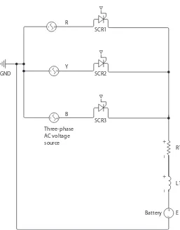
In this section, the interactive model development process is explained with an example of a power electronic converter model. This method is the same irrespective of whether a power electronic converter component-level or sys-tem-level model is used. To encompass all the sources/components specified in Table 2.1, a three-phase half-wave silicon controlled rectifier (SCR) con-verter is considered here [2]. Figure 2.1 shows a three-phase SCR half-wave converter. A three-phase 120 V root mean square (RMS) line-to-neutral, 60 Hz AC voltage source is used. The parameters used for the model are tabu-lated in Table 2.2.
In Figure 2.1, the three-phase AC voltage sources R, Y and B are connected to the anodes of SCRs SCR1, SCR2 and SCR3, respectively. The cathodes of these three SCRs are tied together and connected to a single-phase load com-prising R1, L1 and E. The gate pulse firing angle α for SCR1 in Phase R is 90°. The gate pulse firing angle for SCR2 in Phase Y will be (α + 120) and that for SCR3 in Phase B will be (α + 240)°. A suitable amplitude for the gate pulse depends on the SCR gate turn-on threshold voltage, and a suitable gate pulse width is provided that depends on the data sheet for the relevant SCR. These gate drives for the three SCRs are not shown in Figure 2.1 for clarity. The interactive model development for this converter is explained next.
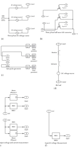
Figure 2.2 shows the interactive model of the three-phase SCR half-wave controller and Figure 2.3 shows the same model with interactive blocks. Figure 2.4a–f shows the various subsystems used in the model shown in Figure 2.2. These are explained as follows:
GND
Three-phase AC voltage source
B Y
SCR2
SCR3
Battery E
L1 R1
+
–
+
–
SCR1 R
– +
– +
– +
– +
FIGURE 2.1
Three-phase half-wave SCR converter.
TABLE 2.2
Model Parameters
Sl. No. Parameter Value Unit
1 RMS line-to-neutral input voltage 120 Volts
2 Frequency 60 Hertz
3 Gate drive amplitude 10 Volts
4 Gate drive frequency 60 Hertz
5 SCR firing angle for reference phase 90 Degrees
6 Load resistance 0.5 Ohms
7 Load inductance 6.5e−3 Henries
1
be understood by referring to the circuit schematic) load subsystem is shown in Figure 2.4d, consisting of a resistor, inductor and a DC voltage source all connected in series. The output voltage and current measurement subsystem is shown in Figure 2.4e, where RMS and MEAN value measurement blocks are used to display the RMS and mean or average value of the output voltage and currents. The input AC voltage measurement block is shown in Figure 2.4f, consisting of an RMS measurement block to display the RMS value of the line-to-neutral input voltage. Detailed interactive model formation is dis-cussed in the following sections.
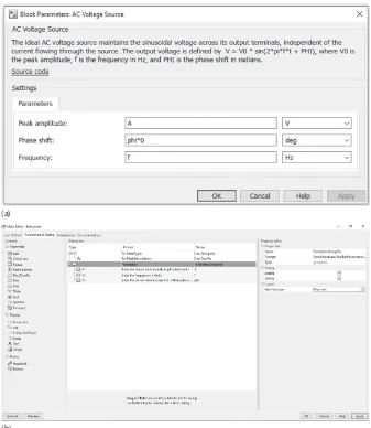
2.3.2 Three-Phase AC Voltage Source
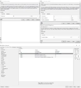
The three-phase AC voltage source subsystem is shown in Figure 2.4a. The dialogue box relating to the AC voltage source module connected to Phase R is shown in Figure 2.5a. The peak amplitude variable is entered as ‘A’ in volts. The phase shift is entered as ‘phi * 0’ in degrees. The frequency is entered as ‘f’ in hertz. In the AC Voltage Source1 module relating to Phase Y and the AC Voltage Source2 module relating to Phase B, the entry corresponding to the phase shift is entered as ‘phi*(−1)’ and ‘phi*(1)’ (or ‘phi*(−2)’), respectively, with all other entries as previously. The following procedure is used to make the three-phase AC voltage source model interactive.
• Step 1: In Figure 2.2, before masking, which appears like Figure
2.4a, select AC Voltage Source, AC Voltage Source1 and AC Voltage Source2 using the mouse pointer. Then, click Diagram → Subsystem and Model Reference → Create Subsystem from the selection to form a subsystem called ‘Three-Phase AC Voltage Source’.
FIGURE 2.3
13
Fundamentals of Interactive Modelling
– +
AC voltage source1
PS S
DC voltage source 1
AC voltage source2
Three-phase AC voltage source
Gate pulse generator
Three-phase half wave SCR converter
Rle load Mean
(Phasor)1
Mean (Phasor)
Output voltage and current measurement Input AC voltage Measurement RMS AC voltage source
R
3 Conn3 3 Conn3
5
• Step 2: Select the subsystem marked ‘Three-Phase AC Voltage Source’, and then click Diagram → Mask → Create Mask. This opens the Mask Editor.
• Step 3: In the Mask Editor, click Parameters and Dialog → Edit. • Step 4: Click or select ‘Parameters’ and enter the instructions to the
user.
(a)
(b)
FIGURE 2.5
15
Fundamentals of Interactive Modelling
• Step 5: Click or select ‘Parameter Group Var’ and enter the variable name used in the subsystem for the particular parameter.
• Step 6: Repeat Steps 4 and 5 until all parameter variable names
are entered for the particular subsystem. Then click the ‘Apply’ button.
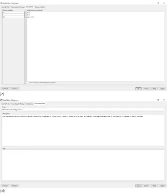
A view of the ‘Parameters and Dialog’ menu completed for the ‘Three-Phase AC Voltage Source’ subsystem is shown in Figure 2.5b. • Step 7: Click ‘Initialization’ in the Mask Editor.
(c)
(d)
FIGURE 2.5
• Step 8: Ensure all parameter group variables are displayed on the left-hand side.
• Step 9: In the ‘Initialization commands’ box, enter the condition to be satisfied for each parameter variable. This can be a parameter vari-able greater than zero or lying within a range or above, below or equal to a particular value. Then click the ‘Apply’ button.
• A view of the ‘Initialization’ menu completed for the ‘Three-Phase AC Voltage Source’ subsystem is shown in Figure 2.5c.
• Step 10: Click ‘Documentation Menu’ in the Mask Editor. • Step 11: In the ‘Type’ box, enter the name of the subsystem.
• Step 12: In the ‘Description’ box, enter the details of the subsystem, the pop-up menu and the value to be entered in each pop-up menu with units.
• Step 13: In the ‘Help’ box, provide any other information relating to the subsystem that the user may need. Clicking the ‘Help’ but-ton opens up this dialogue box. If there is no other information, the ‘Help’ box can be left blank. Then click the ‘Apply’ and ‘OK’ buttons.
The ‘Documentation’ menu for the three-phase AC voltage subsystem is shown in Figure 2.5d.
2.3.3 SCR Three-Phase Half-Wave Converter
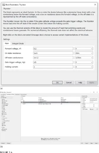
The three-phase half-wave SCR converter subsystem is shown in Figure 2.4b. The dialogue box relating to Thyristor connected to Phase R is shown in Figure 2.6a. Here, only one parameter, which is the gate trigger volt-age, is entered as ‘vth’ in volts. The thyristor will be turned ON only if the gate cathode voltage exceeds this gate trigger voltage ‘vth’. For Thyristor1 and Thyristor2 in phases Y and B, the same value, ‘vth’, is entered for the gate trigger voltage. The following procedure is used to make the SCR three-phase half-wave converter model interactive.
Step 1: In Figure 2.2, select the SCRs marked Thyristor, Thyristor1 and
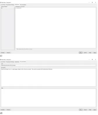
Thyristor2 using the mouse pointer. Then, click Diagram → Subsystem and Model Reference → Create Subsystem from Selection to form a subsystem called ‘SCR Three-Phase Half-Wave Converter’. Then, follow Steps 2 to 6 in Section 2.3.2. A view of the ‘Parameters and Dialog’ menu completed for the SCR three-phase half-wave converter subsystem is shown in Figure 2.6b.
Then, follow Steps 7 to 9 in Section 2.3.2 to open and complete the ‘Initialization commands’ box. The ‘Initialization commands’ box completed for the SCR three-phase half-wave converter is shown in Figure 2.6c.
17
Fundamentals of Interactive Modelling
(a)
(b)
FIGURE 2.6
2.3.4 Gate Pulse Generator
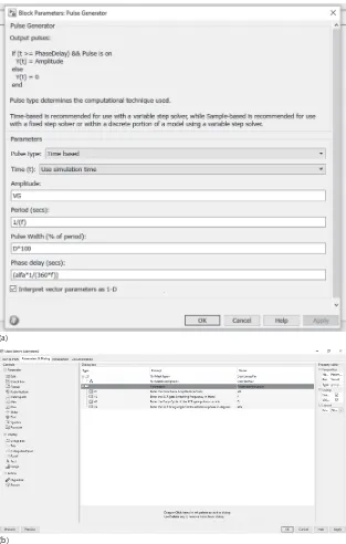
The gate pulse generator subsystem is shown in Figure 2.4c. The dialogue box relating to the pulse generator connected to the gate of Thyristor in Phase R is shown in Figure 2.7a. Here, the various parameters are pulse ampli-tude ‘VG’ in volts, pulse period 1/(f) in seconds where ‘f’ is the frequency of the gate pulse in hertz, pulse width or duty cycle as a ratio of the pulse period and phase delay alfa in degrees. In the dialogue box in Figure 2.7a, ‘Amplitude’ is entered as ‘VG’ V, ‘Period’ is entered as 1/(f) s, ‘Pulse Width’ is
(c)
(d)
FIGURE 2.6
19
Fundamentals of Interactive Modelling
(a)
(b)
FIGURE 2.7
entered as ‘D*100’ and ‘Phase delay’ is entered as ‘(alfa*1/(360*f))’ s. For Pulse Generator1, connected to the gate of Thyristor1 in Phase Y, the phase delay is entered as ‘(alfa*1/(360*f) + 1/(3*f))’, and for Pulse Generator2, connected to Thyristor2 in Phase B, the phase delay is entered as ‘(alfa*1/(360*f) + 2/(3*f))’, respectively, with all other entries the same as for the pulse generator con-nected to the gate of Thyristor in Phase R. The following procedure is used to make the gate pulse generator model interactive.
(c)
(d)
FIGURE 2.7
21
Fundamentals of Interactive Modelling
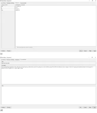
Step 1: In Figure 2.2, select the ‘Pulse Generator’, ‘Pulse Generator1’ and ‘Pulse Generator2’ modules using the mouse pointer. Then click Diagram → Subsystem and Model Reference → Create Subsystem from the selection to create a subsystem called ‘Gate Pulse Generator’. Then, follow Steps 2 to 6 in Section 2.3.2. A view of the ‘Parameters and Dialog’ menu completed for the gate pulse generator subsystem is shown in Figure 2.7b.
Then, follow Steps 7 to 9 in Section 2.3.2 to open and complete the ‘Initialization commands’ box. The ‘Initialization commands’ box completed for the ‘Gate Pulse Generator’ subsystem is shown in Figure 2.7c.
Finally, follow Steps 10 to 13 given in Section 2.3.2 to complete all the dia-logue boxes in the ‘Documentation’ menu. A view of the ‘Documentation’ menu completed for the ‘Gate Pulse Generator’ subsystem is shown in Figure 2.7d.
2.3.5 RLE Load
The RLE load subsystem is shown in Figure 2.4d. This consists of a series-connected resistor, inductor and DC voltage source. The dialogue boxes for the resistor, inductor and DC voltage source are shown in Figure 2.8a–c, respectively. The parameter variable names used for the resistor, inductor and DC voltage source are R1, L1 and E, with units of ohms, henries and volts, respectively.
The following procedure is used to make the RLE load model interactive.
Step 1: In Figure 2.2, select the Resistor, Inductor and DC Voltage source modules using the mouse pointer. Then, click Diagram → Subsystem and Model Reference → Create Subsystem from Selection to create a subsystem called ‘RLE Load’. Then, follow Steps 2 to 6 in Section 2.3.2. A view of the ‘Parameters and Dialog’ menu completed for the RLE load subsystem is shown in Figure 2.8d.
Then, follow Steps 7 to 9 in Section 2.3.2 to open and complete the ‘Initialization commands’ box. The ‘Initialization commands’ box completed for the RLE load subsystem is shown in Figure 2.8e.
Finally, follow Steps 10 to 13 given in Section 2.3.2 to complete all the dia-logue boxes in the ‘Documentation’ menu. A view of the ‘Documentation’ menu completed for the RLE load subsystem is shown in Figure 2.8f.
2.3.6 Output Voltage and Current Measurement
The following procedure is used to make the output voltage and current measurement model interactive.
Step 1: In Figure 2.2, select the RMS, MEAN(Phasor), RMS1 and
MEAN(Phasor)1 modules using the mouse pointer. Then, click Diagram → Subsystem and Model Reference → Create Subsystem from Selection to cre-ate a subsystem called ‘Output Voltage and Current Measurement’.
Then, follow Steps 2 to 6 in Section 2.3.2. A view of the ‘Parameters and Dialog’ menu completed for the output voltage and current measurement subsystem is shown in Figure 2.9c.
(d) (a)
(b)
(c)
FIGURE 2.8
23
Fundamentals of Interactive Modelling
Then, follow Steps 7 to 9 in Section 2.3.2 to open and complete the ‘Initialization commands’ box. The ‘Initialization commands’ box com-pleted for the output voltage and current measurement subsystem is shown in Figure 2.9d.
Finally, follow Steps 10 to 13 given in Section 2.3.2 to complete all the dia-logue boxes in the ‘Documentation’ menu. A view of the ‘Documentation’ menu completed for the output voltage and current measurement subsystem is shown in Figure 2.9e.
(f ) (e)
FIGURE 2.8
2.3.7 Input Voltage Measurement
The three-phase AC input voltage line-to-neutral RMS value measurement subsystem is shown in Figure 2.4f. This consists of an RMS line-to-neutral input voltage measurement block called RMS2. The parameter used is the input frequency ‘f’ in hertz. The dialogue box is the same as shown in Figure 2.9a. The following procedure is used to make the input voltage mea-surement model interactive.
(c)
(a) (b)
FIGURE 2.9
25
Fundamentals of Interactive Modelling
Step 1: In Figure 2.2, select the RMS2 module using the mouse pointer.
Then click Diagram → Subsystem and Model Reference → Create Subsystem from Selection to create a subsystem called ‘Input Voltage Measurement’. Then, follow Steps 2 to 6 in Section 2.3.2. A view of the ‘Parameters and Dialog’ menu completed for the input voltage measurement subsystem is shown in Figure 2.10a.
(e) (d)
FIGURE 2.9
Then, follow Steps 7 to 9 in Section 2.3.2 to open and complete the ‘Initialization commands’ box. The ‘Initialization commands’ box com-pleted for the input voltage measurement subsystem is the same as shown in Figure 2.9d.
Finally, follow Steps 10 to 13 in Section 2.3.2 to complete all the dia-logue boxes in the ‘Documentation’ menu. A view of the ‘Documentation’ menu completed for the input voltage measurement subsystem is shown in Figure 2.10b.
(e) (a)
FIGURE 2.10
27
Fundamentals of Interactive Modelling
2.4 Simulation Results
A simulation of the three-phase half-wave SCR converter model shown in Figure 2.2 was carried out for the parameters shown in Table 2.2. The ode23t(stiff trapezoidal) solver is used [1]. The simulation results for the three-phase AC input voltage are shown in Figure 2.11a–c. The load current and output voltage are shown in Figure 2.12a,b. The simulation results are also tabulated in Table 2.3.
FIGURE 2.11
Three-phase half-wave SCR converter. (a) Line-to-neutral input voltage in volts: Phase R. (b) Line-to-neutral input voltage in volts: Phase Y. (c) Line-to-neutral input voltage in volts: Phase B.
FIGURE 2.12
2.5 Discussion of Results
An interactive model consumes less time compared with a conventional model to simulate and obtain results when there are one or more parameter changes. For example, with a conventional model, if there is a change in the firing angle α, the three pulse generators connected to the gate of the three SCRs have to be opened and the necessary changes in the three dialogue boxes have to be made. This comes to three mouse clicks and three erase and re-enter operations. With an interactive model, it comes to one mouse click and one erase and re-enter operation. Similarly, if there is a change in the input frequency and corresponding thyristor switching frequency, 11 mouse clicks and 11 erase and re-enter operations are required with a con-ventional model, whereas only four mouse clicks and four erase and re-enter operations are required with an interactive model. For a change in the input line-to-neutral voltage, three mouse clicks and three erase and re-enter opera-tions are required with a conventional model, whereas only one mouse click and one erase and re-enter operation are required with an interactive model. Thus, there is a saving in time, especially when there are a large number of models to be tested for various input parameters. Interactive model devel-opment takes more time compared with a conventional model develdevel-opment. But, once an interactive model is developed, the saving in time when testing the model for changes in the input parameters is a definite advantage. If the model topology has one or more capacitors, then variable names starting with C/c, CF/cf, C1/c1, C2/c2 and so on can be given and an interactive model can be developed as for the RLE load subsystem shown in Section 2.3.5.
2.6 Conclusions
Interactive modelling capability is a feature available in the Simulink soft-ware. The entire model is developed using the electrical block set in the Simscape foundation library and Semiconductor block set in the power
TABLE 2.3
Simulation Results for Three-Phase Half-Wave SCR Converter: α = 90°
Sl. No.
RMS Line-to-Neutral Input
Voltage (V)
Input Frequency
(Hz)
RMS Output Voltage
(V)
Average Output Voltage (V)
RMS Load Current
(A)
Average Load Current
(A)
29
Fundamentals of Interactive Modelling
systems library. With Simscape and Simulink block set components, S to PS converters and PS to S converters have to be connected. Also, with Simscape components, the Solver Configuration block has to be connected to achieve simulation. The method of developing an interactive model with a three-phase SCR half-wave converter example is presented in this chap-ter. The method can be easily extended to any power electronic converter topology. With interactive models, the saving in time when testing a power converter for varying parameters is a definite advantage. A virtual power electronics laboratory can be developed with interactive models and, hence, is suitable in an industrial and in a research and development environment.
References
1. Math Works Inc.: “MATLAB/SIMULINK user guide”, R2016b, 2016.
31
3
Interactive Models for AC to DC Converters
3.1 Introduction
In this chapter, the building of interactive models for AC to DC con-verters, also known as rectifiers, is presented. Rectifier circuits can be classified either as half-wave or full-wave bridge rectifiers using semi-conductor diodes, or as controlled half-wave or full-wave bridge rectifiers using silicon-controlled rectifiers (SCRs) or thyristors. Modern rectifiers use bipolar junction transistors (BJTs), metal oxide semiconductor field-effect transistors (MOSFETs), insulated gate bipolar transistors (IGBTs) and gate turn-off thyristors (GTOs). Here, interactive system models for single-phase full-wave diode bridge rectifiers (FWDBRs), full-wave con-trolled bridge rectifiers (FWCBRs) using SCRs and three-phase FWDBRs are developed. The switching function concept is used to develop these models. These models have pop-up menus or dialogue boxes where the required data relating to the AC to DC converter are entered by the user. These system models use Simulink® blocks that solve the governing equa-tions relating to the relevant AC to DC converter. No semiconductor circuit component is used in the model.
3.2 Single-Phase Full-Wave Diode Bridge Rectifier
The single-phase FWDBR circuit schematic is shown in Figure 3.1 [1–4]. The resistive load or RLE load selection using SS1 is shown for convenience only. Let the applied AC voltage VS be of the form VS = Vm* sin(ω.t). During the
positive half-cycle of VS, diodes D1 and D2 conduct from 0 to π, and during
the negative half-cycle, diodes D3 and D4 conduct from π to 2π. The essential derivations of the output voltage are given here for purely resistive load [1].
Vo_avg= 1*
∫
vm.sin( ) ( )
. .t d .t =2.Vm 0π ω ω π
π
I V
The output voltage derivations are shown for RLE load [1–4].
L di
dt R i E V t
O
O m
. + . + = .sin
( )
ω. (3.5)The solution of Equation 3.5 is given here:
i V
3.2.1 Interactive Model for Single-Phase FWDBR with Purely Resistive or with RLE Load
The system model for the single-phase FWDBR is shown in Figure 3.2 [5]. The purely resistive or RLE load selection is combined in one model. The various dialogue boxes are shown in Figure 3.3, where the user can enter
D1
Vs = Vm*sin(w.t)
R
L
E
FIGURE 3.1
33
1/L1_LOAD UDC I_R_LOAD
UDC_AVERAGE Top part Rle_load parameters.
Bottom part R_load parameters. LOAD_SELECT
the appropriate data required. One model can be used for different sys-tem parameters. In Figure 3.2, the selector switch can be double-clicked to select either the purely resistive load or the RLE load option. The value of the line-to-neutral root mean square (RMS) voltage, frequency, the value of RLE loads or that of the purely resistive load used are entered in the appropriate dialogue boxes in Figure 3.3. These values are tabulated in Table 3.1.
The various subsystems of this model are shown in Figure 3.4a–h. These are described as follows.
The single-phase sine-wave AC voltage source in Figure 3.4a is from the ‘Sources’ block in the ‘Simulink’ block set. The dialogue box for this is shown in Figure 3.3. The line-to-neutral RMS voltage in volts and the frequency in hertz are entered in this dialogue box. This line-to-neutral RMS voltage and frequency are internally multiplied by 1.414 and 2π, respectively. This
TABLE 3.1
Single-Phase FWDBR Parameters
Sl. No. Parameter Value
1 Line-to-neutral RMS voltage 120 V
2 Supply frequency 60 Hz
3 RLE load 2.5 Ω, 6.5e−3 H, 10 V
4 Purely resistive load 25 Ω
FIGURE 3.3
35
Interactive Models for AC to DC Converters
sine-wave output is passed to Relay1 in Figure 3.4b. Relay1 is a zero-crossing comparator whose output is the switch function SF, defined in Equation 3.7. The inverse switch function SF_BAR is generated using a switch from the Signal Routing block set, defined in Equation 3.8:
SF for
The switch generating SF_BAR has 0 and 1 as its first u(1) input and third
u(3) input, respectively, while the control or second u(2) input is SF. The switch threshold is 0.5. The switch output is u(1) when input u(2) is greater than or equal to threshold value, else its output is u(3). SF and SF_BAR are passed to the control input u(2) of Switch1 and Switch2, respectively, in Figure 3.4b. The
u(1) input to Switch1 is the AC supply voltage VS, while that for Switch2 is the
negative of this supply voltage, −VS. The u(3) inputs to Switch1 and Switch2
are both zero. The threshold values for Switch1 and Switch2 are both 0.5. The Switch1 and Switch2 outputs are +VS and –VS when their respective u(2)
input is greater than or equal to the threshold value, else their outputs are zero. The output of Switch1 and Switch2 are added using the Add block. The output of this Add block is the rectified DC output voltage Udc (Vdc). ln3 Multiply1 Out1
1
Referring to Figure 3.4b, the output voltage of the sum block Udc can be
expressed as follows:
U V V
In Equation 3.9, VS is the sine-wave input voltage.
The type of load select module shown in Figure 3.4c has two constants, 1 and 0, as input to the single pole double throw (SPDT) switch. Double-clicking the SPDT switch in Figure 3.2 selects either the purely resistive load or the RLE load.
Figure 3.4d, e corresponds to the dialogue box for load resistance data and RLE load data, respectively, shown in Figure 3.3.
If the SPDT switch is thrown to 0 in Figure 3.2, then the purely resistive load R_LOAD is selected. Referring to Figure 3.4f, it is seen that the Divide4 block calculates 1/(R_LOAD), which is passed to the u(3) input of Switch3. The 1/(L1_LOAD) input from Figure 3.4h is passed to the u(1) input of Switch3. The control input u(2) for Switch3 is from the SPDT switch con-nected to the output of Figure 3.4c. The threshold for Switch3 is 0.5, and out-put is either 1/(L1_LOAD) or 1/(R_LOAD), depending on whether the u(2) input is 1 or 0, respectively. The u(2) input of Switch3 is also connected to the S input and through a NOT gate to the R input of the S–R flip-flop, as shown in Figure 3.4f. If the SPDT switch is thrown to 0 or 1, the S–R flip-flop enables the bottom display or top display, respectively, in Figure 3.2.
With SPDT in the 0 or bottom position, the value 1/(R_LOAD) is selected. In Figure 3.4g, the DC output voltage Udc is multiplied by 1/(R_LOAD) and by
RESET, which is 1, using the Multiplier1 block to obtain the DC load current Idc.
If the SPDT switch is thrown to 1, then the RLE load in Figure 3.4e is selected. Referring to Figure 3.4h, it is seen that the Divide2 block calculates 1/(L1_ LOAD), which is applied to the u(1) input of Switch3 in Figure 3.4f. Referring to Figure 3.4f, the u(2) input of this Switch3 is 1, which is greater than its thresh-old of 0.5 and selects output 1/(L1_LOAD). This u(2) input also sets the S–R flip-flop and Q is HIGH and enables the top display for the RLE load.
In Figure 3.4h, the Add1, Multiply1, Multiply2 and Integrator blocks solve Equation 3.5 and the resulting output of the Integrator is the DC load current
Idc with RLE load. The S–R latch enables the top display in Figure 3.2. The
RMS and average value of load voltage Udc and the mean and RMS value of
the load current and the average power output are displayed.
3.2.2 Simulation Results
37
Interactive Models for AC to DC Converters
resistive load are shown in Figure 3.5a–c and those for RLE load are shown in Figure 3.6a–c. The meter readings observed are tabulated in Table 3.2 for both cases.
FIGURE 3.5
(a) Single-phase FWDBR with purely resistive load-source voltage volts. (b) Output voltage volts. (c) Load current in amps.
FIGURE 3.6
(a) Single-phase FWDBR with RLE load-source voltage volts. (b) Output voltage volts. (c) Load current in amps.
TABLE 3.2
Simulation Results for Single-Phase FWDBR
Sl. No.
Type of Load
Udc(RMS) (V)
Udc(AVG) (V)
I_load(RMS) (A)
I_load(AVG) (A)
P_out (W)
1 R only 120 108 4.799 4.321 466.8
3.3 Single-Phase Full-Wave SCR Bridge Rectifier
The single-phase full-wave SCR bridge rectifier is also known as the sin-gle-phase full-wave controlled bridge rectifier (FWCBR) [1–4]. This is shown in Figure 3.7. Assuming pure resistive load, during the positive half-cycle of VS,
thyristors T1 and T2 are fired at an angle α and conduct from α to π. During the negative half-cycle of VS, thyristors T3 and T4 are fired at angle (π + α) and
conduct from (π + α) to 2π. Thus, by varying the firing angle α, the average voltage across the load can be varied. The system model for this FWCBR is developed combining the purely resistive load and RLE load in one model. For the RLE load, continuous load current conduction is assumed. In this case, with the RLE load, thyristors T1 and T2 conduct from α to (π + α) when fired at an angle α during the positive half-cycle of VS and thyristors T3 and
T4 conduct from (π + α) to (2π + α), when fired at an angle (π + α) during the negative half-cycle of VS. This model can be used for continuous conduction
mode only with RLE load.
The essential derivation for output voltage and load current is shown here for purely resistive load.
Vdc = Vm
( ) ( )
t d t Vm
= +
( )
∫
1
1
π ω ω π α
α π
* .sin . . . . * cos (3.10)
T4
Vs=Vm*sin(w.t)
VS R125 R205
65E-3 L1
+
–
10
– –
– –
+ –
T1 T3
T2
SS1 VOUT
E
FIGURE 3.7
39
Interactive Models for AC to DC Converters
Vrms= Vm
( ) ( )
t d t VmAverage input powerP
R V t d t
The essential derivation for output voltage and load current is shown here for RLE load [1].
The solution gives
i V
3.3.1 Model for Single-Phase FWCBR with Purely Resistive or with RLE Load
P load or RLE load voltage selector
Note: Rle_load on top and R_load at bootom. With Rle_load, SCRs must be in continuous conduction mode.
Subsystem3
FIGURE 3.8
41
Interactive Models for AC to DC Converters
the appropriate data required. One model can be used for different system parameters. In Figure 3.8, the selector switch can be double-clicked to select either the purely resistive load or the RLE load option. The value of the line-to-neutral RMS voltage, the frequency, the value of RLE loads used and/or that of the purely resistive load used are entered in the appropriate dialogue boxes in Figure 3.9. These values are tabulated in Table 3.3. The various sub-systems of this model are shown in Figure 3.10a–i. These are described next. The blocks in Figure 3.10a, along with the mux and Fcn block in Figure 3.10b, generate the single-phase sine-wave AC input voltage VS. The dialogue box for this is shown in Figure 3.9. The line-to-neutral RMS voltage (in volts), the frequency (in hertz) and the firing angle α are entered in this dialogue box. The line-to-neutral RMS voltage and frequency are internally multiplied by 1.414 and 2π respectively. Another Fcn1 block in Figure 3.10b generates the delayed sine-wave lagging by firing angle α with respect to the input sine wave. This delayed or lagging sine wave is passed to relay, which generates switch function SF1. The sine-wave input voltage VS from the Fcn block is
passed to Relay1, which generates another switch function SF2. The switch functions SF1 and SF2 are defined in Equations 3.19 and 3.20.
SF
for
for 1
1
0 2
=
( )
≤ ≤(
+)
+
(
)
≤ ≤(
+)
α ω π α
π α ω π α
.
.
t
t
(3.19)
FIGURE 3.9
1
In4 Add In5
5 Product1
43
Interactive Models for AC to DC Converters
SF2
Both Relay and Relay1 are zero-crossing comparators whose output is HIGH or logic 1 when the respective sine-wave input crosses zero and becomes positive, and their output is LOW or logic 0 when the respective sine-wave input crosses zero and goes negative. Switch1 and Switch2 have
u(1) input +VS and 0, u(3) input 0 and −VS, respectively, and the u(2) input for
both is SF1. Both switches have a threshold value of 0.5. Switches 1 and 2 output +VS and 0 when their respective u(2) input is greater than or equal to
the threshold value, else their outputs are 0 and −VS, respectively. Referring
to the mode of connection of Switch1 and Switch2 in Figure 3.10b, the respec-tive outputs of Switch1 and 2 can be mathematically expressed as follows:
Output of Switch Out1 3=SF1.VS (3.21)
Output of Switch Out2 6= −(1 SF1).(−VS) (3.22)
Switch1 and 2 output and SF2 are passed to the u(1), u(3) and u(2) input of Switch3, respectively, in Figure 3.10c. The threshold for Switch3 is 0.5 and output Switch1 value if u(2) input SF2 is greater than or equal to this thresh-old value, else output Switch2 value. The output of Switch3 in Figure 3.10c can be expressed mathematically as follows:
Output of Switch3 Out1 SF . SF= 2( 1. ) (VS + −1 SF2 1).( −SF1).(−VS) (3.23)
The output of Switch3 can be expressed as follows from Equations 3.19, 3.20 and 3.23:
Output of Switch3 Out1 for
for
Equation 3.24 represents the output voltage of single-phase FWCBR with purely resistive load. In Figure 3.10c, the output of the Add1 block can be expressed as follows:
Output of Add1 block Out2 for
for
The type of load select module shown in Figure 3.10d has two constants, 1 and 0, as input to the SPDT switch. Double-clicking the SPDT switch in Figure 3.8 selects either the purely resistive load or the RLE load.
Figure 3.10e, f corresponds to the dialogue box for pure load resistance data and RLE load data, respectively, shown in Figure 3.9.
If the SPDT switch is thrown to 1, then purely resistive load is selected. The Switch3 and Add1 block output of Figure 3.10c and the SPDT output of Figure 3.10d are applied to the u(1), u(3) and u(2) input of Switch4 in Figure 3.10g. Switch4 has a threshold value of 0.5, and selects the purely resistive load volt-age or RLE load voltvolt-age as output depending on its u(2) input corresponding to whether the SPDT switch is 1 or 0. This Switch4 output and SPDT output are passed as u(3) and u(2) input to Switch5, whose u(1) input is 0. Switch5 has a threshold value of 0.5 and its output is 0 if its u(2) input corresponding to the SPDT switch is 1, and outputs the Switch4 value when its u(2) input is 0. Thus, the Switch5 output is always the load voltage corresponding to the RLE load. The Switch4 output can be either the purely resistive or the RLE load voltage, depending on the position of the SPDT switch. The SPDT switch output is inverted using a NOT gate to enable selection of the RLE load.
Referring to Figure 3.10h, the Divide1 block calculates 1/(R1_LOAD), which is passed to the u(1) input of Switch7, whose u(3) input is 0, and the u(2) input is from the SPDT switch output. The threshold is 0.5, and Switch7 output is either 1/(R1_LOAD) or 0, depending on whether the u(2) input corresponding to the SPDT switch is 1 or 0. The Switch4 output from Figure 3.10g is passed to the
u(1) input of Switch6, whose u(3) input is 0, and the u(2) input is the output of the SPDT switch. The threshold for Switch6 is 0.5, and the output is the purely resistive load voltage or 0, depending on whether the u(2) input corresponding to the SPDT switch output is 1 or 0. The Product3 block multiplies the Switch6 and Switch7 outputs, giving a DC load current with a purely resistive load.
RLE load is selected by throwing SPDT to 0. Referring to Figure 3.10f, g and i, it is seen that Switch4 and Switch5 output the load voltage across the RLE load. The Divide2 block calculates 1/(L_LOAD). The Add block, along with the Divide2, Product1, Product2 and Integrator blocks, solves Equation 3.16 to find the load current through the RLE load. Using the NOT gate in Figure 3.10g connected to the SPDT switch, the upper indicating meters are enabled for the RLE load and the lower indicating meters are enabled for the purely resistive load.
3.3.2 Simulation Results
45
Interactive Models for AC to DC Converters
TABLE 3.3
Single-Phase FWCBR Simulation Parameters
Sl. No. Parameter Value
1 Line-to-neutral RMS voltage 120 V
2 Supply frequency 60 Hz
3 RLE load 0.5 Ω, 6.5e−3 H, 10 V
4 Purely resistive load 25 Ω
5 Firing angle α π/3 rad
FIGURE 3.11
Single-phase FWCBR. Alfa is pi/3 radians. Red, input AC voltage; magenta, DC output voltage; green, DC load current for purely resistive load.
FIGURE 3.12
3.4 Three-Phase Full-Wave Diode Bridge Rectifier
The three-phase FWDBR schematic is shown in Figure 3.13. It is used for high-power applications. The diodes are numbered in conduction sequences and each diode conducts 120°. The conduction sequences for the diodes are: D1–D2, D3–D2, D3–D4, D5–D4, D5–D6, D1–D6, D1–D2 and so on, giving six pulses of ripples at the output voltage. The pair of diodes that are connected between that pair of lines having the highest amount of instantaneous line-to-line voltage will conduct [1–4].
The essential derivation for the purely resistive load is shown here [1–4]:
V V t
The average output voltage Vdc is derived as follows [1–4]:
V V t d t
1 R only 107.5 81.07 4.301 3.243 262.9
47
Interactive Models for AC to DC Converters
The RMS output voltage Vrms is derived as follows [1–4]:
V V t d t
If the load resistance is purely resistive, the peak or maximum current through the diode is Im= √3.Vm/R, where R is the load resistance. The RMS
value of the diode current is derived as follows:
I I t d t
The RMS value of the supply current or line current is derived as follows:
where Im is the peak value of the three-phase line current (in Equations 3.30
and 3.31).
If Ls is the source inductance in each of the three phases and f is the
sup-ply frequency, then the average reduction in output voltage due to source or commutating inductances is given as follows [1–4]:
V
X=6. . .
f L I
S dc (3.32)where Idc is the load current.
3.4.1 Model for Three-Phase FWDBR with Purely Resistive Load
Before describing the subsystems in detail, the development of the system model for the three-phase FWDBR is explained as follows:
The system model for the three-phase FWDBR is developed based on refer-ence [6]. The Heaviside function gk for k = 1, 2, 3, … is defined in Figure 3.14. This Heaviside function determines whether the diode is conducting or in the blocking state [6]. In Figure 3.13, e1, e2 and e3 are the arm voltages and u1, u2 and u3 are the phase voltages. The relations connecting them are given here:
e1 = g1*Vdc (3.33)
e2 = g2*Vdc (3.34)
e3 = g3*Vdc (3.35)
u1 = f1*Vdc (3.36)
u2 = f2*Vdc (3.37)
ik 1
gk
0
FIGURE 3.14
49
Load voltage average Idc amps
Load voltage rms Mean
abc ud idq0
id dq0 to abc1
abc to dq2
abc to dq1 Subsystem1
u3 = f3*Vdc (3.38)
The DC current is given here:
Idc=g i1 1. +g i2 2. +g i3 3. mation is defined as given here:
x