1
Transistor and Component
Models at Low and High
Frequencies
1.1
Introduction
Equivalent circuit device models are critical for the accurate design and modelling of RF components including transistors, diodes, resistors, capacitors and inductors. This chapter will begin with the bipolar transistor starting with the basic T and then the π model at low frequencies and then show how this can be extended for use at high frequencies. These models should be as simple as possible to enable a clear understanding of the operation of the circuit and allow easy analysis. They should then be extendible to include the parasitic components to enable accurate optimisation. Note that knowledge of both the T and π models enables regular switching between them for easier circuit manipulation. It also offers improved insight.
As an example S21 for a bipolar transistor, with an fT of 5GHz, will be calculated and compared with the data sheet values at quiescent currents of 1 and 10mA. The effect of incorporating additional components such as the base spreading resistance and the emitter contact resistance will be shown demonstrating accuracies of a few per cent.
The harmonic and third order intermodulation distortion will then be derived for common emitter and differential amplifiers showing the removal of even order terms during differential operation.
The chapter will then describe FETs, diode detectors, varactor diodes and passive components illustrating the effects of parisitics in chip components.
It should be noted that this chapter will use certain parameter definitions which will be explained as we progress. The full definitions will be shown in Chapter 2. Techniques for equivalent circuit component extraction are also included in Chapter 2.
1.2
Transistor Models at Low Frequencies
1.2.1
‘T’ Model
Considerable insight can be gained by starting with the simplest T model as it most closely resembles the actual device as shown in Figure 1.1. Starting from a basic NPN transistor structure with a narrow base region, Figure 1.1a, the first step is to go to the model where the base emitter junction is replaced with a forward biased diode.
The emitter current is set by the base emitter junction voltage The base collector junction current source is effectively in parallel with a reverse biased diode and this diode is therefore ignored for this simple model. Due to the thin base region, the collector current tracks the emitter current, differing only by the base current, where it will be assumed that the current gain, β, remains effectively constant.
C
E B
re
βib ib
C
E B
βib ib
N
P
N
E B
C
(a) (b) (c)
Figure 1.1 Low frequency ‘T’ model for a bipolar transistor
distortion in a common emitter and differential amplifier. Here, however, we will concentrate on the low frequency small signal AC ‘T’ model which takes into account the DC bias current, which is shown in Figure 1.1c. Here re is the AC resistance of the forward biased base emitter junction.
The transistor is therefore modelled by an emitter resistor re and a controlled current source. If a base current, ib, is applied to the base of the device a collector current of βib flows through the collector current source. The emitter current, IE, is therefore (1+β)ib. The AC resistance of re is obtained from the differential of the diode equation. The diode equation is:
−
=
exp
1
kT
eV
I
I
E ES (1.1)where IES is the emitter saturation current which is typically around 10-13
, e is the charge on the electron, V is the base emitter voltage, Vbe, k is Boltzmann’s constant and T is the temperature in Kelvin. Some authors define the emitter current, IE, as the collector current IC. This just depends on the approximation applied to the original model and makes very little difference to the calculations. Throughout this book equation (1) will be used to define the emitter current.
Note that the minus one in equation (1.1) can be ignored as IES is so small. The AC admittance of re is therefore:
=
kT
eV
I
kT
e
dV
dI
ES
exp
(1.2)Therefore:
dI
dV
e
kT
I
=
(1.3)The AC impedance is therefore:
dV
dI
kT
e I
=
.
1
(1.4)As k = 1.38
×
10-23, T is room temperature (around 20o
C) = 293K and e is 1.6
×
10-19I
dI
dV
r
mA e
25
≈
=
(1.5)This means that the AC resistance of re is inversely proportional to the emitter current. This is a very useful formula and should therefore be committed to memory. The value of re for some typical values of currents is therefore:
1mA
≈
25
Ω
10mA
≈
2 5
.
Ω
25mA
≈
1
Ω
It would now be useful to calculate the voltage gain and the input impedance of the transistor at low frequencies and then introduce the more common π model. If we take a common emitter amplifier as shown in Figure 1.2 then the input voltage across the base emitter is:
(
)
b ein
i
r
V
= β
+
1
.
(1.6)β
i
bR
LC
E
B
i
bFigure 1.2 A common emitter amplifier
(
)
(
) (
)
mA e
b e b
b in in
I
r
i
r
i
i
V
Z
=
=
1
+
β
=
1
+
β
=
1
+
β
25
(1.7)The forward transconductance, gm, is:
(
)
e eb b
in out m
r
r
i
i
V
I
g
1
1
≈
+
=
=
β
β
(1.8)
Therefore:
e m
r
g
≈
1
(1.9)and:
e L L
m in
out
r
R
R
g
V
V
−
=
−
=
(1.10)Note that the negative sign is due to the signal inversion.
Thus the voltage gain increases with current and is therefore equal to the ratio of load impedance to re. Note also that the input impedance increases with current gain and decreases with increasing current.
In common emitter amplifiers, an external emitter resistor, Re, is often added to apply negative feedback. The voltage gain would then become:
e e
L
in out
R
r
R
V
V
+
=
(1.11)1.2.2
The
π
Transistor Model
The ‘T’ model can now be transformed to the π model as shown in Figure 1.3. In the π model, which is a fully equivalent and therefore interchangeable circuit, the input impedance is now shown as (β+1)re and the output current source remains the same. Another format for the π model could represent the current source as a voltage controlled current source of value gmV1. The input resistance is often called rπ.
βib
C
C
E
E E
B
B
re
ib
ib
(β+1)re V1 β i o r g Vb m 1
Figure 1.3 T to π model transformation
At this point the base spreading resistance rbb’ should be included as this incorporates the resistance of the long thin base region. This typically ranges from around 10 to 100Ω for low power discrete devices. The node interconnecting rπ
and rbb’ is called b’.
1.3
Models at High Frequencies
C
E E
B
1
V
b
Cb 'e Cb 'c I
rb'e rb b'
β irb 'e o r g Vm 1 ib
1
Figure 1.4 Hybrid π model
A more complete model including the package characteristics is shown in Figure 1.5. The typical package model parameters for a SOT 143 package is shown in Figure 1.6. It is, however, rather difficult to analyse the full model shown in Figures 1.5 and 1.6 although these types of model are very useful for computer aided optimisation.
Figure 1.6. Typical model for the SOT143 package. Obtained from the SPICE model for a BFG505. Data in Philips RF Wideband Transistors CD, Product Selection 2000 Discrete
Semiconductors.
We should therefore revert to the model for the internal active device for analysis, as shown in Figure 1.4, and introduce some figures of merit for the device such as fβ and fT. It will be shown that these figures of merit offer significant information but ignore other aspects. It is actually rather difficult to find single figures of merit which accurately quantify performance and therefore many are used in RF and microwave design work. However, it will be shown later how the S
parameters can be obtained from knowledge of fT.
It is worth calculating the short circuit current gain h21 for this model shown in Figure 1.4. The full definitions for the h, y and S parameters are given in Chapter 2. h21 is the ratio of the current flowing out of port 2 into a short circuit load to the input current into port 1.
I
I
h
b c
=
21 (1.12)
(
)
1
1
1
' ' '
'
'
=
+
+
+
⋅
=
CR
j
i
r
C
C
j
i
r
i
be b c b e b
b e b e
rb
ω
ω
(1.13)
where the input and feedback capacitors add in parallel to produce C and the rb’e becomes R. The collector current is IC = β irb’e, where we assume that the current through the feedback capacitor can be neglected as ICb’c << βirb’e. Therefore:
1
1
21
+
=
+
=
=
SCR
h
SCR
i
I
h
feb
c
β
(1.14)
Note that β and hfe are both symbols used to describe the low frequency current gain.
A plot of h21 versus frequency is shown in Figure 1.7. Here it can be seen that
the gain is constant and then rolls off at 6dB per octave. The transition frequency fT occurs when the modulus of the short circuit current gain is 1. Also shown on the graph, is a trace of h21 that would be measured in a typical device. This change in
response is caused by the other parasitic elements in the device and package. fT is therefore obtained by measuring h21 at a frequency of around fT/10 and then extrapolating the curve to the unity gain point. The frequency from which this extrapolation occurs is usually given in data sheets.
F re qu ency A
A ctual device m easurem ent
hfe f
β(3dB p oint)
f w h e n h = 1T 2 1 M e asure f for h extrapo lationT 2 1
The 3 dB point occurs when ωCR = 1. Therefore:
f
CR
β
=
π
1
2
CR
=
f
1
2
π
β (1.15)and h21 can also be expressed as:
β
f
f
j
h
h
fe+
=
1
21 (1.16)
As fT is defined as the point at which
h
21=
1
, then:2
1
1
1
+
=
=
+
β
β
f
f
h
f
f
j
h
T fe
T fe
(1.17)
( )
feT
h
f
f
22
1
=
+
β
(1.18)
( )
21
2
−
=
fe
T
h
f
f
β
(1.19)
As:
( )
h
fe 2>>
1
(1.20)CR
h
f
h
f
T fe feπ
β
2
.
=
Note also that:
fe T
h
f
f
β=
(1.22)As:
β
f
f
j
h
h
fe+
=
1
21 (1.16)
it can also be expressed in terms of fT :
T fe fe
f
f
h
j
h
h
.
1
21
+
=
(1.23)Take a typical example of a modern RF transistor with the following parameters:
fT = 5 GHz and hfe = 100. The 3dB point for h21 when placed directly in a common
emitter circuit is fβ = 50MHz.
Further information can also be gained from knowledge of the operating current. For example, in many devices, the maximum value of fT occurs at currents of around 10mA. For these devices (still assuming the same fT and hfe) re = 2.5Ω, therefore rb’e ≈250Ω and hence CT ≈ 10pF with the feedback component of this being around 0.5 to 1pF.
For lower current devices operating at 1mA (typical for the BFT25) re is now around 25Ω, rb’e around 2,500Ω and therefore CT is a few pF with Cb’e
≈
0.2pF.Note, in fact, that these calculations for CT are actually almost independent of
hfe and only dependent on IC, re or gm as the calculations can be done in a different way. For example:
T
fe
f
h
f
CR
=
1
2
π
β=
2
π
(1.24)(
fe)
e Tfe
r
h
f
h
C
1
2
+
=
π
Tm
e
T
f
g
r
f
π
π
2
2
1
=
≈
(1.25)Many of the parameters of a modern device can therefore be deduced just from fT,
hfe, Ic and the feedback capacitance with the use of these fairly simple models.
1.3.1
Miller Effect
fT is a commonly used figure of merit and is quoted in most data sheets. It is now worth discussing fT in detail to find out what other information is available.
1. What does it hide? Any output components as there is a short circuit on the output.
2. What does it ignore? The effects of the load impedance and in particular the Miller effect. (It does include the effect of the feedback capacitor but only into a short circuit load.)
It is important therefore to investigate the effect of the feedback capacitor when a load resistance RL is placed at the output. Initially we will introduce a further simple model.
If we take the simple model shown in Figure 1.8, which consists of an inverting voltage amplifier with a capacitive feedback network, then this can be identically modelled as a voltage amplifier with a larger input capacitor as shown in Figure 1.8b. The effect on the output can be ignored, in this case, because the amplifier has zero output impedance.
Figure 1.8a Amplifier with feedback C Figure 1.8.b Amplifier with increased input C
(
)
V
c=
V
in−
V
out (1.26)If the voltage gain of the amplifier is -G then the voltage across the capacitor is therefore:
(
V
GV
)
V
(
G
)
V
c=
in+
in=
in1
+
(1.27)The current through the capacitor, Ic, is therefore IC = Vc jωC. The change in input admittance caused by this capacitor is therefore:
(
)
(
)
I
V
V j C
V
V
G j C
V
G j C
c
in c
in
in
in
=
ω
=
1
+
ω
= +
1
ω
(1.28)The capacitor in the feedback circuit can therefore be replaced by an input capacitor of value (1 + G)C. This is most easily illustrated with an example. Suppose a 1V sinewave was applied to the input of an amplifier with an inverting gain of 5. The output voltage would swing to –5V when the input was +1V therefore producing 6V (1 + G) across the capacitor. The current flowing into the capacitor is therefore six times higher than it would be if the same capacitor was on the input. The capacitor can therefore be transferred to the input by making it six times larger.
1.3.2
Generalised ‘Miller Effect’
Note that it is worth generalising the ‘Miller effect’ by replacing the feedback component by an arbitrary impedance Z as shown in Figure 1.8c and then investigating the effect of making Z a resistor or inductor. This will also be useful when looking at broadband amplifiers in Chapter 3 where the feedback resistor can be used to set both the input and output impedance as well as the gain. It is also worth investigating the effect of changing the sign of the gain.
Vin
Vin
Vo u t
Vo u t
-G
-G Z
(1 + G ) Z
As before:
(
)
inZ
G
V
V
=
1
+
(1.29)As:
Z
V
I
ZZ
=
(1.30)the new input impedance is now:
(
G
)
Z
I
V
Z in
+
=
1
(1.31)as shown in Figure 1.8d. If Z is now a resistor, R, then the input impedance becomes:
(
G
)
R
+
1
(1.32)This information will be used later when discussing the design of broadband amplifiers.
If Z is an inductor, L, then the input impedance becomes:
(
G
)
L
j
+
1
ω
(1.33)
As before, if Z was a capacitor then the input impedance becomes:
(
G
)
C
j
+
−
1
ω
(1.34)(
G
)
R
−
1
(1.35)which produces a negative resistance when G is greater than one.
1.3.3
Hybrid
π
Model
It is now worth applying the Miller effect to the hybrid π model where for convenience we make the current source voltage dependent as shown in Figure 1.9.
C
E E
B
1
V
b
Cb 'e
Cb 'c I
rb'e
rb b'
β irb 'e o r g Vm 1
ib
1
Figure 1.9 Hybrid π model for calculation of Miller capacitance
Firstly apply the Miller technique to this model. As before it is necessary to calculate the input impedance caused by Cb’c. The current flowing into the collector load, RL, is:
1 1
I
V
g
I
c=
m+
(1.36)where the current through Cb’c is:
(
V
V
)
C
j
ω
I
1=
1−
0 b'c.
(1.37)The feedforward current I1 through the feedback capacitor Cb’c is usually small compared to the current gmV1 and therefore:
1 0
g
R
V
Therefore:
(
V
g
R
V
)
C
j
ω
I
1=
1+
m L 1 b'c.
(1.39)(
g
R
)
C
j
ω
V
I
1=
11
+
m L b'c.
(1.40)The input admittance caused by Cb’c is:
(
g
R
)
C
j
ω
V
I
c b L
m
.
1
'1 1
=
+
(1.41)
which is equivalent to replacing Cb’c with a shunt capacitor in parallel with Cb’e to produce a total capacitance:
(
m L)
bc beT
g
R
C
C
C
=
1
+
'+
' (1.42)The model generated using the Miller effect is shown in Figure 1.10. Note that this model is an approximation in this case, as it is only effective for calculating the forward transmission and the input impedance. It is not useful for calculating the output impedance or the reverse transmission or stability. This is only because of the approximation used when deriving the output voltage. If the load is zero then the current gain would be as derived when h21 was calculated.
Vin R s
B
E
CT
C
E rb b '
rb e ib
β irb 'e o r g Vm 1
Figure 1.10 Hybrid π model incorporating Miller capacitor
in s bb T e b e b T e b e b
V
R
r
j
C
r
r
j
C
r
r
V
+
+
+
+
=
' ' ' ' ' 11
1
ω
ω
(1.43)(
)(
)
inT e b s bb e b e b
V
j
C
r
R
r
r
r
+
+
+
=
ω
' ' ' '1
(1.44)Expanding the denominator:
(
)(
)
inT e b s bb s bb e b e b
V
j
C
r
R
r
R
r
r
r
V
+
+
+
+
=
ω
' ' ' ' ' 1 (1.45) As:a
b c
a
b
c
b
+
=
+
1
(1.46)
(
)
ins bb e b e b s bb T s bb e b e b
V
R
r
r
r
R
r
C
j
R
r
r
r
V
+
+
+
+
+
+
=
' ' ' ' ' ' ' 11
1
ω
(1.47) As: 1V
R
g
V
out=
−
m L (1.48)(
)
(
)
+
+
+
+
+
+
−
=
s bb e b e b s bb T s bb e b e b L m in outR
r
r
r
R
r
C
j
R
r
r
r
R
g
V
V
' ' ' ' ' ' '1
1
ω
(1.49) Note that:(
)
j
C
R
R
r
r
r
R
r
C
j
T s bb e b e b s bb Tω
ω
=
+
+
+
+
+
1
1
1
1
' ' ' ' (1.50) where:(
)
s bb e b e b s bbR
r
r
r
R
r
R
+
+
+
=
' ' ' ' (1.51)This is effectively rbb’ in series with RS all in parallel with rb’e which is the effective Thévenin equivalent, total source resistance seen by the capacitor. The first two brackets of equation (1.49) show the DC voltage gain and the third bracket describes the roll-off where:
(
m L)
bc beT
g
R
C
C
C
=
1
+
'+
' (1.52)The numerator of the third bracket produces the 3dB point when the imaginary part is equal to one.
[ ]
(
)
1
2
' ' ' ' 3=
+
+
+
s bb e b e b s bb T dBR
r
r
r
R
r
C
f
π
(1.53)The full equation is:
(
)
[
1
]
(
)
1
2
' ' ' ' ' '3
+
+
=
Therefore from equation (1.53):
[ ]
(
)
s bb e b e b s bb T dBR
r
r
r
R
r
C
f
+
+
+
=
' ' ' ' 32
1
π
(1.55)[ ]
T(
bb s)
be s bb e b dBr
R
r
C
R
r
r
f
' ' ' ' 32
+
+
+
=
π
(1.56) As:(
)
[
m L bc be]
T
g
R
C
C
C
=
1
+
'+
' (1.52)(
)
[
m L bc be]
(
bb s)
bes bb e b dB
r
R
r
C
C
R
g
R
r
r
f
' ' ' ' ' ' 31
2
+
+
+
+
+
=
π
(1.57)Note that using equation (1.51) for R:
(
)
[
g
R
C
C
]
R
f
e b c b L m dB ' ' 31
2
1
+
+
=
π
(1.58)1.4
S
Parameter Equations
This equation describing the voltage gain can now be converted to 50Ω S
parameters by making RS= RL= 50Ω and calculating S21 as the value of Vout when Vin is set to 2V. The equation and explanation for this are given in Chapter 2. Equation (1.49) therefore becomes:
1.5
Example Calculations of
S
21It is now worth inserting some typical values, similar to those used when h21 was investigated, to obtain S21. Further it will be interesting to note the added effect caused by the feedback capacitor. Take two typical examples of modern RF transistors both with an fT of 5GHz where one transistor is designed to operate at 10mA and the other at 1mA. The calculations will then be compared with theory in graphical form.
1.5.1
Medium Current RF Transistor – 10mA
Assume that fT = 5GHz, hfe = 100, Ic=10mA, and the feedback capacitor, Cb’c ≈ 2pF. Therefore
r
e=
2
.
5
Ω
andr
b'e≈
250
Ω
. Letr
bb'≈
10
Ω
for a typical 10mAdevice. The 3dB point for h21 (short circuit current gain) when placed directly in a
common emitter circuit is fβ = fT/hfe. Therefore fβ = 50MHz. As:
CR
f
=
1
2
π
β (1.24)then
CR
=
3
.
18
×
10
−9As h21 is the short circuit current gain Cb’c and Cb’e are effectively in parallel. Therefore:
pF
6
.
12
' '+
=
=
C
beC
bcC
(1.61)As
pF
C
b'c≈
1
C
b'e=
12
.
6
−
1
=
11
.
6
pF
(1.62)However, CT for the measurement of S parameters includes the Miller effect because the load impedance is not zero. Thus:
(
)
bc bee L e
b c b L m
T
C
C
r
R
C
C
R
g
C
1
' '1
'+
'
+
=
+
+
(
1
+
20
)
1
+
11
.
6
=
32
.
6
pF
=
T
C
(1.64)As:
[ ]
T(
bb s)
be s bb e b dBr
R
r
C
R
r
r
f
' ' ' ' 32
+
+
+
=
π
(1.65)then:
[
32
.
6
10
]
(
10
50
)
250
2
50
10
250
12
3
×
+
+
+
=
−π
dB
f
= 101MHz (1.66)The value of S21 at low frequencies is therefore:
(
)
+
+
=
50
2
' ' ' 21 bb e b e b L mr
r
r
R
g
S
(1.67)( )
32
.
25
50
10
250
250
20
2
21
=
+
+
=
S
(1.68)A further modification which will give a more accurate answer is to modify re to include the dynamic diode resistance as before but now to include an internal emitter fixed resistance of around 1Ω which is fairly typical for this type of device. This would then make re = 3.5Ω and rb’e = 350Ω. For the same fT and the same feedback capacitance the calculations can be modified to obtain:
pF
9
' '+
=
=
C
beC
bcC
AsC
b'c≈
1
pF
andC
b'e=
9
−
1
=
8
pF
(1.69)(
1
14
.
3
)
1
8
23
.
3
pF
1
'+
'=
+
+
=
+
=
bc bee L
T
C
C
r
R
C
(1.70)As:
then:
[
]
(
)
f
E
dB
3
350 10 50
2
23 3
12 10 50 350
=
+
+
−
+
π
.
= 133MHz (1.71)The low frequency S21 is therefore:
(
)
+
+
=
50
50
.
.
2
' '
' 21
bb e b
e b m
r
r
r
g
S
(1.72)( )
24
.
4
50
10
350
350
3
.
14
.
2
21
=
+
+
=
S
(1.73)This produces an even more accurate answer. These values are fairly typical for a transistor of this kind, e.g. the BFR92A. This is illustrated in Figure 1.11 where the dotted line is the calculation and the discrete points are measured S parameter data.
Note that the value for the base spreading resistance and the emitter contact resistance can be obtained from the SPICE model for the device where the base series resistance is RB and the emitter series resistance is RE.
10 100 1.103 1.104 0.1
1 10 100
S 21
Frequency, MHz
1.5.2
Lower Current Device - 1mA
If we now take a lower current device with the parameters fT = 5GHz, hfe = 100,
Ic=1mA, and the feedback capacitor, Cb’c
≈
0.2pF
,r
e=
25
Ω
andr
b'e≈
2500
Ω
.
Let rbb’ ≈ 100Ω for a typical 1mA device. The 3dB point for h21 (short circuit
current gain) when placed directly in a common emitter circuit is:
hfe
f
f
=
Tβ (1.22)
Therefore fβ = 50MHz
CR
h
f
h
f
T fe feπ
β
2
.
=
=
(1.21)Note also that:
CR
f
=
1
2
π
β (1.74)Therefore
CR
=
3
.
18
×
10
−9As h21 is the short circuit current gain, Cb’c and Cb’e are effectively in parallel. Therefore:
pF
26
.
1
' '+
=
=
C
beC
bcC
(1.75)As
C
b'c≈
0
.
2
pF
pF
06
.
1
2
.
0
26
.
1
'e
=
−
=
bC
(1.76)However, CT for the measurement of S parameters includes the Miller effect because the load impedance is not zero. Therefore:
(
)
bc bee L e
b c b L m
T
C
C
r
R
C
C
R
g
C
1
' '1
'+
'
+
=
+
+
(
1
+
2
)
0
.
2
+
1
.
06
=
1
.
66
pF
=
T
C
(1.78)As:
[ ]
T(
bb s)
be s bb e b dBr
R
r
C
R
r
r
f
' ' ' ' 32
+
+
+
=
π
(1.65) then:[
1
.
66
10
]
(
100
50
)
2500
2
50
100
2500
12
3
×
+
+
+
=
−π
dB
f
= 678MHz (1.79)The low frequency value for S21 is therefore:
(
)
+
+
=
50
50
.
2
' ' ' 21 bb e b e b mr
r
r
g
S
(1.72)( )
3
.
77
50
100
2500
2500
2
2
21
=
+
+
=
S
(1.80)As before an internal emitter fixed resistance can be incorporated. For these lower current smaller devices a figure of around 8Ω is fairly typical. This would then make re = 33Ω and rb’e = 3300Ω. For the same fT and the same feedback capacitance the calculations can be modified to obtain:
pF
96
.
0
' '+
=
=
C
beC
bcC
(1.81)As:
C
b'c≈
0
.
2
pF
pF
76
.
0
2
.
0
96
.
0
'e
=
−
=
bC
(1.82)(
1
1
.
52
)
0
.
2
0
.
76
1
.
26
pF
1
'+
'=
+
+
=
+
=
bc bee L
T
C
C
r
R
As:
[ ]
T(
bb s)
be s bb e b dBr
R
r
C
R
r
r
f
' '
' ' 3
2
+
+
+
=
π
(1.65)then:
[
1
.
26
10
]
(
100
50
)
3300
2
50
100
3300
12 3
+
×
+
+
=
−π
dB
f
=880MHz
The low frequency S21 is therefore:
(
)
+
+
=
50
50
.
2
' '
' 21
bb e b
e b m
r
r
r
g
S
(1.84)( )
+
+
=
50
100
3300
3300
52
.
1
2
21S
=2.91
(1.85)These values are fairly typical for a transistor of this kind operating at 1mA. Calculated values for S21 and measured data points for a typical low current device,
such as the BFG25A, are shown in Figure 1.12.
10 100 1.103 1.104
0.1 1 10
S21
Frequency, MHz
It has therefore been shown that by using a simple set of models a significant amount of accurate information can be gained by using fT, hfe, the feedback capacitance and the operating current.
In summary the low frequency value of S21 is therefore:
(
)
e L L
m bb
e b
e b L
m
r
R
R
g
r
r
r
R
g
S
2
2
50
.
2
' '
'
21
≈
≈
+
+
=
(1.86)and the 3dB point is:
[ ]
T(
bb s)
be s bb e b dBr
R
r
C
R
r
r
f
' '
' ' 3
2
+
+
+
=
π
(1.65)where:
e b c b e
L
T
C
C
r
R
C
1
'+
'
+
=
1.83)1.6
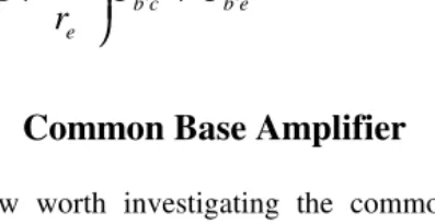
Common Base Amplifier
It is now worth investigating the common base amplifier where the base is grounded, the input is connected to the emitter and the output is connected to the collector. This is most easily shown using the T model as shown in Figure 1.13. The π model is included in Figure 1.14.
re ( + 1 )iβ b
ib
βib Ie
E
B
C
B
( + 1 )r
β
ei
bβ
i
bI
eE
B
C
Figure 1.14 The π model for common base
The input impedance at the emitter is:
e
in
r
Z
=
(1.87)The voltage gain is therefore:
(
)
eL
e b L b
in out
r
R
r
i
R
i
V
V
≈
+
=
1
β
β
(1.88)
Note that this is non-inverting. The current gain is:
(
+
1
)
=
≈
1
=
α
β
β
b b
in out
i
i
I
I
(1.89)
The major features of this type of circuit are:
1. The negligible feedback C. Further the grounded base also partially acts as a screen for any parasitic feedback.
2. No current gain, so the amplifier gain can only be obtained through an increase in impedance from the input to the output.
1.7
Cascode
It is often useful to combine the features of the common emitter and common base modes of operation in a Cascode transistor configuration. This is shown in Figure 1.15.
Figure 1.15 Cascode configuration
There are a number of useful features about the Cascode:
1. The capacitance between B and C is very low. Further as the base of Q2 is
grounded this acts as a screen to any parasitic components. 2. The input impedance Zin at B of Q2 is:
)
mA
(
25
1
e m e
I
g
r
=
=
(1.90)This is quite low.
3. This means that the Miller effect on Q1 is small. Further the voltage gain of
Q1 is:
1
−
=
−
=
m e AB
g
r
V
V
(1.91)
4. The input impedance at A of Q1 is:
(
) (
)
mA
25
1
1
I
r
i
V
Z
eb in
in
=
=
+
β
=
+
β
(1.92)5. The voltage gain is:
e L L
m in
out
r
R
R
g
V
V
=
−
=
−
(1.93)6. The current gain is β.
This device therefore offers the input impedance of a single transistor common emitter stage with an input capacitance of:
(
)
[
m L bc be]
[
( )
bc be]
T
g
R
C
C
C
C
C
=
1
+
'+
'=
2
'+
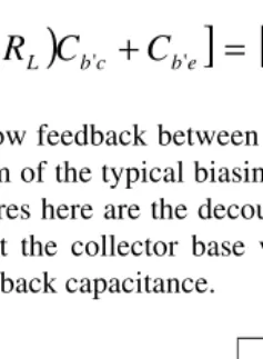
' (1.94)but with very low feedback between the input and output typically of the order of 20fF. A diagram of the typical biasing for a Cascode is shown in Figure 1.16. The important features here are the decoupling on the base of Q2 to ensure a good AC ground and that the collector base voltage of Q1 should be sufficiently large to ensure low feedback capacitance.
1.8
Large Signal Modelling – Harmonic and Third Order
Intermodulation Distortion
So far linear models have been presented and it has been shown how significant information can be obtained from simple algebraic analysis. Here the simple model, shown earlier in Figure 1.1b, will now be used to demonstrate large signal modelling of a bipolar transistor in both common emitter and differential mode. The harmonic and third order intermodulation products will be deduced. It will then be shown how differential circuits suppress even order terms such as the second and fourth harmonics.
The simple model consists of a current controlled current source in the base collector region and a diode in the base emitter region. The distortion in the emitter current will be analysed. The collector current is then assumed to be αIE where
α = β/(β + 1). It will be assumed that the collector load circuit will not cause significant other products. This is a reasonable assumption for small voltage swings well away from collector saturation.
1.8.1
Common Emitter Distortion
Taking the transistor in common emitter mode and applying a DC bias and AC signal, the emitter current becomes:
−
+
=
exp
sin
1
T BIAS ES
E
V
t
V
V
I
I
ω
(1.95)where VT = kT/e ≈ 25mV at room temperature. Separating the DC bias and the AC signal components into separate terms [2]:
≈
−
=
T DC
ES T
T BIAS ES
E
V
t
V
I
I
V
t
V
V
V
I
I
exp
.
exp
sin
ω
0exp
sin
ω
(1.96)+
+
+
=
t
V
V
t
V
V
I
I
T T DCE
ω
ω
2 2
0
1
sin
1
2
sin
(1.97)
+
+
t
V
V
t
V
V
T Tω
ω
4 4 3 3sin
24
1
sin
6
1
Expanding the higher order terms to obtain the harmonic frequencies gives:
+
−
+
+
=
2
2
cos
1
2
1
sin
1
2 0t
V
V
t
V
V
I
I
T T DC Eω
ω
(1.98)−
+
+
4
3
sin
sin
3
6
1
3t
t
V
V
Tω
ω
−
−
+
4
4
cos
5
.
0
2
cos
2
5
.
1
24
1
4t
t
V
V
Tω
ω
(1.98)There are a number of features that can be seen directly from this equation: 1. All the harmonics exist where, for example, the second harmonic is
produced from the square law term.
2. The even order terms produce even order harmonics and terms at DC so the DC bias increases with the signal amplitude.
3. The odd order terms produce signals at the fundamental frequency as well as at the harmonic frequency so even if the harmonics are filtered out there is also non-linearity in the fundamental term.
5. The DC term is therefore dependent on IDC0, the second and fourth order terms:
+
+
=
4 2 064
1
4
1
1
T T DC EV
V
V
V
I
I
(1.99)Note that this analysis is still an approximation because transistors are usually biased via resistors, which means that the assumptions produce errors as the signals increase.
The signal distortion is usually quoted in terms of a ratio of the unwanted signal over the original input signal and therefore this equation should be normalised by dividing by V/VT. The order of the amplitude term is therefore one order below the order of the distortion. Therefore the distortion products normalised to the fundamental frequency become:
Fundamental 1 + 3rd order term
2
8
1
TV
V
(1.100)Second Harmonic
t
V
V
Tω
2
cos
4
1
+ 4th order term
3
48
1
TV
V
(1.101)Third Harmonic
t
V
V
Tω
3
sin
24
1
2
(1.102)Fourth Harmonic
t
V
V
Tω
4
cos
192
1
3
(1.103)1.8.2
Third Order Intermodulation Products
Let the input signal be two sine waves of equal amplitude:
t
V
e
B
and
t
V
e
A
T T 2 1sin
sin
ω
=
ω
=
(1.104)As:
(
)
3 3 3 2 23
3
A
B
AB
B
A
B
A
+
=
+
+
+
(1.105)=
+
3 2 1sin
sin
t
V
e
t
V
e
T Tω
ω
(1.106)(
t
t
t
t
t
t
)
V
e
T 2 2 1 2 1 2 2 3 1 3 3sin
sin
3
sin
sin
3
sin
sin
ω
+
ω
+
ω
ω
+
ω
ω
(1.106)
Expanding these terms produces (1.107):
(
)
(
)
[
]
t
+
t
+
−
t
t
+
−
t
t
V
e
T 1 2 2 1 2 3 1 3 3sin
2
cos
1
sin
2
cos
1
2
3
sin
sin
ω
ω
ω
ω
ω
ω
As:
(
)
(
)
[
t
t
]
t
t
2 1 2 1 21
sin
2
sin
2
2
1
sin
2
cos
ω
ω
=
ω
−
ω
−
ω
+
ω
−
(1.108)and:
(
)
(
)
[
t
t
]
t
t
1 2 1 2 12
sin
2
sin
2
2
1
sin
2
cos
ω
ω
=
ω
−
ω
−
ω
+
ω
−
(1.109)(
)
(
)
(
)
[
]
(
)
(
)
[
]
+
+
+
−
−
+
−
+
+
+
+
t
t
t
t
t
t
t
t
V
e
T 1 2 2 1 1 2 2 1 2 3 1 3 2 1 32
sin
2
sin
4
3
2
sin
2
sin
4
3
sin
sin
sin
sin
2
3
ω
ω
ω
ω
ω
ω
ω
ω
ω
ω
ω
ω
(1.110)Taking just the inband terms in the middle row of equation (1.110), the amplitude of the terms will therefore be:
4
3
.
6
1
(1.111) Therefore:(
)
t
Sin
(
)
t
Sin
V
e
T 1 2 2 1 32
2
.
8
1
ω
ω
ω
ω
−
+
−
(1.112)Normalising this to the fundamental input tones by dividing by e/VT produces:
(
)
t
(
)
t
V
e
T 1 2 2 1 22
sin
2
sin
.
8
1
ω
−
ω
+
ω
−
ω
(1.113)
Two tones each at 1mV would therefore produce a distortion level of 0.02% and two tones at 10mV would produce 2% TIR.
Therefore from this equation a number of parameters can be deduced
1. Third order intermodulation distortion applied to two tones produces in-band signals which are at frequencies of (2ω1
–
ω2) and (2ω2–
ω1). Forexample, two tones at 100 and 101MHz will produce distortion products at 99 and 102MHz. Note similarly that fifth order intermodulation products produce (3ω1
–
2ω2) and (3ω2–
2ω1).fifth and seventh order terms which can also come in band. A 1 dB change in input level will cause a 5dB and a 7dB change in distortion level respectively. Note that this can be used as a means to determine the order of intermodulation distortion during faultfinding. The author has often found higher order distortion products in multi-loop frequency synthesisers and spectrum analysers.
3. The change between the fundamental and third order terms changes by a square law such that a 1dB change in input signal produces a 2dB change in the difference between the fundamental signal level and the distortion products.
Values of harmonic and third order intermodulation percentage distortion for a variety of input voltages are given in Table 1.1. For the third order intermodulation distortion, the input voltage for each tone is the same as the single tone value for the harmonic distortion. In other words, the third order distortion for two tones each of value 1mV is 0.02%.
Table 1.1 Harmonic and third order intermodulation distortion for a bipolar transistor
t
ω
0.1mV 0.5mV 1mV 5mV 10mVTIR 2
×
10-6% 5×
10-5% 0.02% 0.5% 2%2ωt 0.1% 0.5% 1% 5% 10%
3ωt 6.7
×
10-5% 1.7×
10-3% 6.7×
10-3% 0.17% 0.67%4ωt 3.3
×
10-8% 4.2×
10-5% 3.3×
10-5% 4.2×
10-3% 0.033%1.8.3
Differential Amplifier
Q1
RC RC
Q2
V
I
I1E E
I2
V
+ V
C C-V
C CFigure 1.17 Differential amplifier
Taking each transistor in turn [2]:
=
T BE ES
E
V
V
I
I
11
1
exp
(1.114)
=
T BE ES
E
V
V
I
I
22
2
exp
(1.115)Assume that the transistors are matched such that IES1 = IES2 then:
−
=
T BE BE
E E
V
V
V
I
I
1 22 1
exp
(1.116)As the total voltage around a closed loop is zero then:
0
2 2 1
1
−
BE+
BE−
I=
I
V
V
V
V
(1.117)ID I I BE
BE
V
V
V
V
V
1−
2=
1−
2=
(1.118)and:
=
T ID E EV
V
I
I
exp
2 1 (1.119)Note also that the current through the current source equals the sum of the emitter currents:
2
1 E
E
EE
I
I
I
=
+
(1.120)(
−
)
=
=
T ID E EE T ID E EV
V
I
I
V
V
I
I
1 2exp
1exp
(1.121)
=
+
T ID EE T ID EV
V
I
V
V
I
11
exp
exp
(1.122)Therefore:
(
)
(
ID T)
T ID EE E
V
V
V
V
I
I
exp
1
exp
1
=
+
(1.123)Multiplying top and bottom by
−
T IDV
V
exp
: (1.124)
+
=
T ID EE EV
V
I
I
exp
1
2 (1.126)To calculate the differential output voltage:
C C CC
O
V
I
R
V
1=
−
1 (1.127)C C CC
O
V
I
R
V
2=
−
2 (1.128)Therefore the differential output voltage is:
C C C C O O
OD
V
V
I
R
I
R
V
=
1−
2=
2−
1 (1.129)
+
−
−
+
=
1
exp
1
1
exp
1
T ID T ID C EE ODV
V
V
V
R
I
V
α
(1.130)where α converts the emitter current to the collector current so:
As:
( )
( )
( )
1
2
exp
1
2
exp
tanh
+
−
=
x
x
x
(1.133)
−
=
T ID C EE ODV
V
R
I
V
2
tanh
α
(1.134) As:( )
3 5 7315
17
15
2
3
1
tanh
x
=
x
−
x
+
x
−
x
(1.135)and assuming that VID is a sine wave, then:
−
+
−
=
sin
...
2
3
1
sin
2
3 3t
V
V
t
V
V
R
I
V
T ID T ID C EEOD
α
ω
ω
(1.136)Taking the ½ outside the bracket and expanding the third order term then:
−
−
+
−
=
...
4
3
sin
sin
3
12
1
sin
2
3t
t
V
V
t
V
V
R
I
V
T ID T ID C EE ODω
ω
ω
α
(1.137) As a check for this equation the small signal gain can be calculated from the linear terms as: C m T C EE IDOD
g
R
V
R
I
V
V
−
=
−
=
2
α
(1.138)Because the emitter current in each transistor is:
2
EE
I
then:
re
V
I
g
T EE m
1
2
≈
=
(1.140)Equations (1.135) and (1.137) demonstrate that:
1. Only odd harmonics exist owing to circuit symmetry. 2. The DC bias does not change.
3. These circuits make good symmetrical limiters.
To calculate the harmonic distortion and third order intermodulation distortion it is necessary to normalise the equations as before by dividing by VID/VT. The third harmonic distortion ratio is therefore:
t
V
V
T
ID
ω
3
sin
48
1
2
(1.141)
The third order intermodulation distortion ratio is therefore:
(
)
t
(
)
t
V
e
T
1 2 2
1 2
2
sin
2
sin
.
16
1
ω
ω
ω
ω
−
+
−
(1.142)
1.9
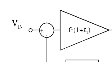
Distortion Reduction Using Negative Feedback
Harmonic and third order intermodulation distortion can be reduced by applying negative feedback. In common emitter and differential amplifiers this is most easily achieved by inserting resistors in the emitter circuit. The estimation of the reduction in distortion can be rather difficult to analyse. It is therefore worth performing a simple generic calculation to see the effect of negative feedback on distortion products.
V
INV
O U T+
β
G (1 + )ε1
-+
Figure 1.18 Model of distortion reduction with negative feedback
The voltage transfer characteristic can be calculated as:
( )
(
ε
)
β
ε
+
+
+
=
1
1
1
G
G
V
V
IN OUT
(1.143)
( )
(
β
)
β
ε
ε
G
G
G
V
V
IN OUT
+
+
+
=
1
1
(1.144)
Dividing the top and bottom by (1 + βG):
( )
(
)
(
G
)
G
G
G
V
V
IN OUT
β
ε
β
β
ε
+
+
+
+
=
1
1
1
1
(1.145)
For:
(
1
+
G
)
<<
1
G
β
ε
β
(1.146)
(
+
) ( )
+
−
(
+
)
=
G
G
G
G
V
V
IN OUT
β
ε
β
ε
β
1
1
1
(
+
)
+
−
+
−
+
=
G
G
G
G
G
G
V
V
IN OUT
β
ε
β
β
ε
β
ε
β
1
1
1
1
2
(1.148)
(
)
(
+
)
−
+
−
+
+
+
+
=
G
G
G
G
G
G
G
G
V
V
IN OUT
β
ε
β
β
ε
β
β
β
ε
β
1
1
1
1
1
1
2
(1.149)
Ignoring square law terms then:
(
+
)
+
+
=
G
G
G
V
V
IN OUT
β
ε
β
1
1
1
(1.150)The error is therefore reduced by:
G
G
G
G
1
.
1
1
1
β
β
=
+
+
(1.151)Which is equal to the ratio of:
gain
loop
Open
gain
loop
Closed
(1.152)
For example, if it is necessary reduce the distortion in an amplifier with a open loop gain of 20 by a factor of 2 then the closed loop gain after feedback should be reduced to 10.
It is now useful to look at the dual gate MOSFET which is an integrated Cascode of two FETs with the added feature that the bias on gate 2 can be used to vary the gain between gate 1 and the output drain by up to 50dB. Initially it is worth investigating the single gate MOSFET.
1.10
RF MOSFETs
MOSFETs, the input or gate terminal is insulated from the channel (usually) by a layer of silicon dioxide. (In the junction FET insulation is produced by a reverse biased junction.) FETs are majority carrier only devices, thus avoiding probl