I ntroductio n to Digital S ignal P rocessing and Digit al Filtering
1.1
Introduction
Digital signal processing (DSP) refers to anything that can be done to a signal using code on a computer or DSP chip. To reduce certain sinusoidal frequency components in a signal in amplitude, digital filtering is done. One may want to obtain the integral of a signal. If the signal comes from a tachometer, the integral gives the position. If the signal is noisy, then filtering the signal to reduce the amplitudes of the noise frequencies improves signal quality. For example, noise may occur from wind or rain at an outdoor music presentation. F iltering out sinusoidal components of the signal that occur at frequencies that cannot be produced by the music itself results in recording the music with little wind and rain noise. Sometimes the signal is corrupted not by noise, but by other signal frequencies that are of no present interest. If the signal is an electronic measurement of a brain wave obtained by using probes applied externally to the head, other electronic signals are picked up by the probes, but the physician may be interested only in signals occurring at a particular frequency. By using digital filtering, the signals of interest only can be presented to the physician.
1.2
Historical Perspective
Originally signal processing was done only on analog or continuous time signals using analog signal processing (ASP). Until the late 1950s digital
Introduction to Digital Signal
Processing and Digital Filtering
computers were not commercially available. When they did become commercially available they were large and expensive, and they were used to simulate the performance of analog signal processing to judge its effectiveness. These simulations, however, led to digital processor code that simulated or performed nearly the same task on samples of the signals that the analog systems did on the signal. After a while it was realized that the simulation coding of the analog system was actually a DSP system that worked on samples of the input and output at discrete time intervals.
But to implement signal processing digitally instead of using analog systems was still out of the question. The first problem was that an analog input signal had to be represented as a sequence of samples of the signal, which were then converted to the computer’s numerical representation. The same process would have to be applied in reverse to the output of the digitally processed signal. The second problem was that because the processing was done on very large, slow, and expensive computers, practical real-time processing between samples of the signal was impossi-ble. Finally, as we will see in Chapter 9, even if digital processing could be done quickly enough between input samples in order to adequately represent the input signal, high sample rates require more bits of precision than slower ones.
The development of faster, cheaper, and smaller input signal samplers (ADCs) and output converters from digital data to analog data (DACs) began to make real-time DSP practical. Also, the processors were becoming smaller, faster, and cheaper and used more bits. Real-time replacements for analog systems may be just as small, cheap, and accurate and be able to process at a sample rate adequate for many analog signals. However, testing and modification of the coding for DSP systems led to DSP systems that have no analog signal processing equivalents, yet sometimes perform the signal processing better than the DSP coding developed to replace analog systems. For digital filtering, these processing methods are discussed in Chapters 10 and 11.
1.3
Simple Examples of Digital Signal Processing
of signals as well as digital integration and digital correlation of signals. This text concentrates on constant rate digital filtering, with references to where the material is applicable to DSP in general. At the end of the text the techniques developed for digital filtering will be used for the DSP task of integration to show how the concepts and techniques are not limited to digital filtering.
The concepts are very simple. A signal is sampled in time at a constant rate in order to input its magnitude value at periodic intervals into the com-puter. The sample value of the analog magnitude is converted into a binary number. The sampling and conversion are done with an analog to digital converter (ADC). Now the computer code can work on the signal. The computer code computes an output value, which is converted to an analog magnitude from a binary number and then held constant until a new out-put is comout-puted to replace it. This is done by a digital to analog converter (DAC). The basic DSP system described here is shown in Figure 1.1. To illustrate the concept of DSP and to see where more study and analysis are needed, let’s look at a few simple things that can be done to a sampled signal. If a signal is sampled every T seconds by an ADC and in the computer the sample value is just multiplied by a constant and then sent to the DAC, you have a digital amplifier. The gain of the amplifier is equal to the coded value of the constant. The following equation describes this digital amplifier, where x is the current input sample value from the ADC and y is the corresponding computer output to the DAC.
y = ax A simple digital amplifier
If the sampled value of the input signal is multiplied by T, you have computed an approximation to the area under the signal between samples, as long as the signal doesn’t change too much between samples. If this value is added to the previous input sample multiplied by T, you
s a m p l e r a n a l o g / b i n
computer
coding
bin/analog hold
ADC DAC
x(t) x y y(t)
have approximated the area under the signal over two sample times. This could be repeated endlessly to approximate the area under the signal from when sampling started, as shown in Figure 1.2. The area under a signal or function is its integral. Thus you have performed very simple digital integration using the current sample of the input multiplied by T and then adding the result to the previous output. This process is described by the following equations after two input samples (the –1 subscripts indicate they are previous input or output values).
y–1 = T x–1 Simple digital integration after one input sample (the previous sample)
y = y–1 + T x Simple digital integration after two input samples (the current sample)
By using looping, such as a “While” or “For” loop, the preceding equations could be repeated endlessly by looping about one equation. If the current input sample value is multiplied by one-half and added to half the previous sample value of the input, a current change in the input signal is reduced, while if the signal is changing slowly the output is very close to the input, since it is just the sum of two half values. Thus the computer is doing a very simple lowpass filtering of the input signal. This simple process is represented by the following equation. The result of using this equation on a string of input samples from the ADC is the input to the DAC shown in Table 1.1. As can be seen, the results, y, are smoothed or lowpass filtered versions of x, the ADC output.
y = 0.5x + 0.5x–1 Simple digital lowpass filtering
x(t)
t
T 2T 3T
area under dashed boxes approximates
area under x(t) after 2 samples at t = 0 and t = T x(0)
x(T) x(2T)
1.4 The Common DSP Equation
The simple DSP examples just discussed were carried out using some input sample values stored in the computer or received currently from the ADC, multiplying them by appropriate constants, and summing the results. Sometimes the previous output values are multiplied by appropri-ate constants and also added to the first sum to give a new output, as was done in the digital integration example. Almost all digital signal process-ing by a computer involves addprocess-ing the signal input sample just obtained, multiplied by a constant, to the sum of a few previous input samples, each multiplied by their corresponding constants, and sometimes adding all of this to a few previous outputs, each multiplied by their constants, to obtain a new output. This leads to the common equation used for almost all DSP:
y =(b−1y−1 +⋅⋅⋅+ b−my−m)+(ax + a−1x−1 +⋅⋅⋅+ a−nx−n) (Equation 1.1) In Equation 1.1, the xs are the sampled input values, the ys are the output samples going to a DAC. The subscripts indicate how many previous sample periods ago are referred to. The as and bs are just constants stored in the computer or DSP chip. A flowchart showing how Equation 1.1 might be implemented by code in the computer shown in Figure 1.1 is given in Figure 1.3.
It may seem strange that almost all DSP tasks are carried out by solving the preceding equation each time a new value of x is input from the ADC, but you must remember that all a computer can do mathematically is add, subtract, multiply, and divide; which is just what this equation requires. If you choose any values for any of the a and b constants and repeat the equation for every new input sample from an ADC, you will be doing DSP! But what DSP have you done and how well? The answers to these questions and more will be given in the rest of this text.
Table 1.1
Example of digital filtering (smoothing)
ADC sample time 0 T 2T 3T 4T
ADC output x 1.2 0.7 1.4 1.1 0.6
1.5 What the DSP Equation Shows
The common DSP equation will be used to show that many DSP questions need further study if one is to understand digital signal processing and do analysis or design of a DSP system. These questions include the following:
◗ How do you choose the a and b coefficients to perform a
spe-cific DSP task, such as doing second-order lowpass Butterworth filtering?
◗ How many coefficients are needed, and what is the effect of
using fewer than required?
◗ Are the b coefficients always needed, and what is the effect if
they are not used?
initialize X1, X2, etc. to 0
wait till ADC returns new sample X
Y = 1.565*Y1 − 0.6438*Y2 + 0.019977X + 0.0395X1 + 0.01977X2
Y2 = Y1 Y1 = Y X2 = X1 X1 = X
send Y to DAC
X1, X2, ... are names for x
X is name for x
Y is name for y, Y1 is name for y , etc.
This is the coded DSP equation etc.
Saving previous values, only 2 shown here
−1, x−2,
−1
◗ The a and b coefficients are represented as binary numbers in
the computer; how many bits should be used to meet the filter specifications?
◗ The x values are sample values of the input signal; how often
should the signal be sampled?
◗ What is the effect of different sample rates, and does the filter
coding need to be changed if the sample rate changes?
◗ How many bits should be used in the ADC and DAC to obtain a
specific precision?
Introduction
In this chapter we examine the effects of sampling on signals and DSP systems. All DSP input signals are sampled, usually at equal intervals of time, in order to input numbers representative of the signal into a computer or DSP chip. We need to determine the effect of this sampling on the signal, as it produces unexpected and critical side effects; these need to be understood before effective filter design can be carried out. In order to simplify the demonstration of the effects of sampling, we will use an analog input signal composed of a single cosine wave. This signal will illustrate and quantitatively show the effects of sampling an analog signal by means of the ADC.
2.1
Periodic Sampling of a Cosine Signal
All signals worked on by DSP systems must be sampled at discrete values of time in order to be input into a DSP chip or computer. This sampling and its conversion to binary values is done by the ADC. This periodic sampling creates very special signal and DSP system characteristics. These characteristics are used in the specification and design of digital filters and DSP systems. In order to see and analyze these characteristics, we will look at the effects of periodic sampling on a cosine signal at different frequencies. We will often refer to signals at, above, or below a certain frequency, rather than to sinusoids with frequencies at, above, or b elow
Effect of Signal Sampling
c h a p t e r
those of sinusoids at a certain frequency. This shorthand English is used almost universally in industry and the literature. As an example, “reduc-ing the frequencies above 100 rad/s” means to reduce the amplitudes of all sinusoids with frequencies above 100 rad/s.
If the signal into an ADC is a cosine wave at the radian frequency of w rad/s, its equation is given by Equation 2.1.
x(t) = cos(wt) (Equation 2.1)
The continuous time variable is t, and A is the peak value. If the signal is sampled every T seconds, its value at the sample times is given by Equation 2.2, where n is an integer.
x(nT ) = cos(wnT ) (Equation 2.2)
This sampling process is illustrated in Figure 2.1, where T = 0.1 and w is 2π rad/s. Column 2 of Table 2.1 gives nT, which is the sample time for every integer n, since the samples occur at t = 0, T, 2T, . . . only. A few sample values are computed in column 3 and can easily be checked using a calculator. All that has been done is to substitute nT for t, as shown in Equation 2.2. This is a valid way to get the equation of any signal after sampling, not just that of the cosine signal used here. For example, the following equations are the input and sampled output signals of an ADC for a decaying sinusoidal signal.
x(t) = Ae–3tcos(7t)
x(n) = x(nT) = Ae–3nT cos(7nT)
Notice that for notational convenience the sampled signal argument is usually written without the sample period T, but T or its value is never left out of the sampled signal equation (or it would be a different equation).
2.2
Periodicity of Any DSP System Frequency Response
Let’s look at the values of the sampled sinusoid when its frequency w is increased by the sampling frequency ws, as shown in the following equation.
x1(t) = cos[(w +ws)t] (Equation 2.3)
The sampling frequency in Hz is 1/T and in rad/s is 2π/T, so Equation 2.3 gives
x1(n) = cos[(w+2π/T)nT]
= cos(wnT + 2nπ)
= cos(wnT) Table 2.1
Notice that after sampling, the signal in Equation 2.3 looks just like the original sampled signal in Equation 2.2. You can see that the sampled values of Equation 2.3 shown in column 4 of Table 2.1 are the same as the values in column 3. The preceding equations make use of the fact that the sine or cosine of an angle offset by 2π is not changed. You can easily see that any angles offset by multiples of 2π are the same by turning around 2π radians in a room and finding that you are facing in the original direction again.
If the cosine signal frequency is increased by integer multiples of the sampling frequency, its sampled values out of the ADC are indistinguish-able from the corresponding values of the samples of the unshifted cosine input to the ADC. This is true even if the original frequency is decreased by multiples of the sampling frequency such that a negative argument for the sampled cosine is obtained, since cos(–a) is cos(a), from trigonome-try. This is also apparent to all students in electronics , since on a scope the only difference between a cosine signal and a negative cosine signal on an oscilloscope is when the trace starts.
Why was it useful to point out that two different cosine signals into an ADC have the same sample values out of the ADC if they differ in frequency by the sampling frequency of 2π/T rad/s? The reason is that all signals worked on by a DSP system are represented in a computer as outputs from an ADC. If two signals have the same values out of the ADC, then any DSP system will do exactly the same thing to both signals. One example is a lowpass digital filter. The purpose of a lowpass filter is to reduce the amplitude of sinusoidal signals above a specified frequency, while not reducing the amplitude below a specified frequency. From the preceding discussion, we know that above a certain frequency the digital lowpass filter will start acting like a highpass filter because a high frequency sinusoidal will have the same sample values as a lower frequency sinusoidal signal. This important fact will be used in Chapter 3 in drawing graphical digital filter specifications.
and the sample values by boxes. If you want to filter an analog signal, you must sample at a high enough rate or eliminate the high frequency content of the signal first.
We have shown that a cosine signal increased in frequency by the ADC sampling rate has the same sample values as if its frequency were not increased. Next it will be shown that its sample values will be the same at an even lower increased frequency. As stated earlier, from trigonometry we have cos(a) = cos(–a). Again using the property that any trigonometric function is identical if its angle is changed by 2π radians, we will show that the signal x2(t) in Equation 2.4 has the same value out of the ADC as the original signal x(t).
x2(t) = cos[(–w + ws)t ] (Equation 2.4)
This cosine signal x2(t) is just the original signal x(t) with its frequency at the sample frequency minus the original signal’s frequency. When samples of x2(t) are taken every T seconds by the ADC, the equation for the sample values is derived as in the following set of equations.
x2(n) = cos[(–w + 2π/T)nT]
= cos(–wnT + 2πn)
= cos(–wnT)
= cos(wnT)
Again it is seen that at a higher frequency even less than the sample frequency the sampled values out of an ADC and into a computer look identical to those at a lower frequency. This can be verified by computing the values in column 5 of Table 2.1 at the sample times on a calculator, using Equation 2.4 with T = 0.1 and w = 2π rad/s. This new higher frequency is not the original increased by the sampling frequency, but the original frequency subtracted from the sample frequency. This result is true for all integer multiples of the sample frequency.
Thus, using the simple algebraic substitution of nT for t to obtain the value of a cosine signal at the sample times separated by T seconds, we have seen that all DSP systems must do the same thing to sinusoids of frequency w as they do to sinusoids at frequencies w above and below the sample frequency, since their sample values into the computer are the same. This is shown in Figure 2.3, where a cosine of amplitude A is plotted at w, ws + w, and ws –w. Remember that ws is just the sampling frequency in rad/s. This significant result must be taken into account when designing a DSP system. If the DSP system is the previously mentioned lowpass filter, its filtering characteristics repeat, as shown in Figure 2.4. When specifying the frequency characteristics of a DSP system such as a digital filter, you must be aware that they will repeat above half the sample rate at π/T in rad/s, as seen in Figure 2.4, and this repetition is periodic.
amplitude of DSP output
frequency rad/s w
w
w s w2 w1
2
s A
2.3
Aliasing and Nyquist Limit
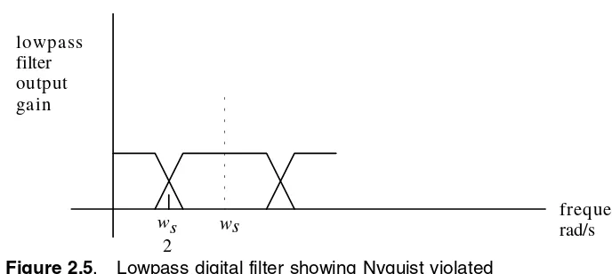
The condition where the highest input signal frequency content is equal to half the sample rate is called the Nyquist limit, and it leads to the Nyquist criterion. The Nyquist criterion is not violated if the sampling rate is more than twice as high as the highest frequency of the sinusoids in the signal, that is, if the highest input signal frequency content is less than the Nyquist limit. This is shown in Figure 2.4. The figure is drawn for an arbitrary input signal frequency spectrum; the signal might be composed of only one cosine wave or many cosine or sine waves.
In Figure 2.4 the Nyquist criterion is not violated, but it can be seen that if the sampling frequency is not greater than twice the highest frequency of any sinusoid in the signal, frequency components in the original signal would look like lower frequency signal components. Figure 2.5 shows the same signal spectrum sampled at a lower rate, so that the Nyquist limit is violated. The DSP system not only treats sinusoids above the Nyquist limit as if they were lower frequency sinusoids, but actually includes them with the actual lower frequency sinusoids. It is important to be aware of this double whammy. The DSP system not only has a periodic frequency spectrum for its output signal, but it also modifies the spectrum you have tried to design by including higher frequency sinusoids for processing as if they were the corresponding lower frequency sinusoids. There is no way to undo this effect of a DSP system. You must either b e aware of the damage and accept the consequences, avoid violating the Nyquist crite-rion by sampling faster, or eliminate frequency components in the signal above the Nyquist limit.
filter output gain
frequency rad/s w
ws 2
s
lowpass
2.4
Anti-aliasing Filters
Because the frequency content of most signals is unknown to some degree, especially when noise is considered, most DSP systems use a lowpass analog filter called an anti-aliasing filter in front of the ADC. This filter must be an analog filter, since it is in front of the ADC. If it were after the ADC it would itself be a digital filter, with the same problems you want to eliminate from the original DSP system! Figure 2.6 shows a typical DSP system using an anti-aliasing filter.
The specifications on the anti-aliasing filter depend on the input signal sinusoidal frequency content and the proposed sampling rate specified by the sample period T. As mentioned earlier, it must be an analog lowpass filter. It seems strange that almost all DSP systems and especially digital filters include an analog filter. However, this is usually a very simple lowpass filter to build. All it needs to do is to reduce the amplitudes of sinusoids in the signal into the ADC below an acceptable level above a frequency at which they look like significant lower frequency sinusoids.
lowpass filter output gain
frequency rad/s ws
ws 2
Figure 2.5. Lowpass digital filter showing Nyquist violated
anti-aliasing filter
LPF
sampler
computer coding analog/bin
x(t) x y y(t)
ADC
hold bin/analog
DAC
Figure 2.7 shows this process for a digital lowpass filter, with the much less stringent anti-aliasing lowpass analog filter response shown in dashed lines.
Example 2.1. Determining the requirements for an anti-aliasing
filter
Problem: Assume that a digital lowpass filter is to be designed to pass all frequencies below 100 rad/s and reduce all frequencies above 500 rad/s by 32. Let’s assume the sample period is 0.001 s. An anti-aliasing filter must be designed for this digital filter.
Solution: The sample rate in rad/s is 2000π. From Figure 2.7 it can be seen that frequencies above 2000π minus 100 rad/s must be reduced by 32 (by the anti-aliasing filter) or else the digital filter will pass them as if they were the corresponding low frequency signals in the passband.
The requirements on the anti-aliasing filter are seen to be that it reduces the amplitude of the signal into the ADC by 32 or more above 5783 rad/s while not significantly reducing the frequencies below 100 rad/s. From an analog filtering course, it can be learned that this is easily achieved by a first-order lowpass analog filter. A first-order filter reduces the signal by 2 every time the frequency doubles beyond the corner frequency. If the corner frequency is set at 100 rad/s, by the time the frequency is 3200 rad/s (which is five doublings of the corner frequency), the analog signal is reduced by 32. This first-order lowpass filter could even be a simple two-component RC filter.
filter output lowpass
gain
frequency rad/s w
ws
2 s
2.5
The Nyquist Limit and DSP Output Periodicity by
Mathematical Means
Most DSP texts and most engineers have been trained to think of aliasing and the Nyquist criterion in terms of the frequency of a sampled signal. A simple derivation is given in the following discussion; most other derivations are much more complex. It is not necessary to determine the magnitude spectrum of a sampled signal, since we have determined aliasing and the Nyquist criterion without it. Inside the computer or DSP chip, there are just a bunch of numbers being manipulated, not a signal with a sampled analog spectrum. But to illustrate the other approach, the following derivation is given, using knowledge from first-semester calculus and Laplace transform theory. The output of an ADC is a sampled signal and we will show that this leads to it having a periodic spectrum with a period of 1/T Hz or 2π/T rad/s. Again, as can be seen in Figure 2.4 and Figure 2.5, this leads to the Nyquist criterion on the sampling rate.
We will use the delta or impulse function δ(t) used in analog signal processing class, a very narrow and tall signal with area (or strength) = 1 at t = 0 and zero value anywhere else. Then δ(t – T) is just a spike of strength 1 at t = T and zero everywhere else. The sum of δ(t) and δ(t – T) is just spikes of strength 1 at t = 0 and another at t = T. Using this approach, the output of an ADC is given by the following equations.
x(nT)= x(n)= x(0)δ(t)+ x(T)δ(t − T)+ x(2T)δ(t − 2T)+ . . .
x(n) =
∑
n=0 ∞x(nT)δ(t − nT) = x(t)
∑
n=0 ∞δ(t − nT)
Now it can be seen that
∑
n=0 ∞δ(t − nT) is periodic (plot it), so it has a Fourier series, as given by the following equation.
∑
n=0 ∞δ(t − nT) = a0 +
∑
k=1 ∞ak cos(kωst) +
∑
k=1 ∞bk sin(kωst), where ωs = 2π/T
a0= 1 T
∫
−T / 2T / 2
∑
n=0 ∞δ(t − nT)dt = 1/T
ak = 2 T
∫
−T / 2T / 2
∑
n=0 ∞δ(t − nT) cos(kωst)dt = 2 T
bk = 2 T
∫
−T / 2T / 2
∑
n=0 ∞δ(t − nT) sin(kωst)dt = 0
Using the preceding coefficients in the Fourier series equation, we can write the equation for the sum of the impulses in the following form.
∑
n=0 ∞δ(t − nT) = 1 T +
2 T
∑
k=1 ∞
cos(kωst)
Using this in the equation for x(nT) = x(n), as a discrete-time signal, gives the following equation.
x(n) = x(t)[1 T +
2 T
∑
k=1 ∞
cos(kωst)]
Now let x(t) be any sinusoid of amplitude A at frequency w. Then the preceding equation for x(n) can be written in the following form.
x(n) = x(nT) = A cos(ωt)[1 T +
2 T
∑
k=1 ∞
cos(kωst)]
Using the trigonometric identity for the product of cosines, we finally have the result we need in the following equation.
x(n) = x(nT) = A
T cos(ωt) + 2 A
T
∑
k=1 ∞[0.5 cos(ω − kωs)t + 0.5 cos(ω + kωs)t]
every ws rad/s or 1/T Hz and looks like Figure 2.3 for any w, where w1 is w + ws and w2 is –w + ws.
Summary
In this chapter the effect of periodic sampling of an analog signal is shown to generate two important characteristics. These characteristics were developed by using a test signal composed of only a cosine wave, but any signal can be considered to be composed of a sum of sinusoids like the cosine wave. This is known from Fourier analysis and is also obvious to students of filtering, since otherwise there would b e no need to design filters to amplify or reduce certain frequencies.
The first important effect of sampling is that any sinusoid that is sampled has the same sample values as a sinusoid offset in frequency by the original signal frequency above and below the sample frequency. Thus the output of any DSP system must be periodic about the sample frequency, and also any multiple of the sample frequency. This is due to the fact that if the sample values are the same when input into the DSP chip or computer, it will do the same thing to them.
The other effect of sampling an analog signal is a result of the repetition of the DSP frequency characteristics just discussed and leads to the Nyquist criterion. If a higher frequency sinusoid is treated in the DSP system the same as a lower frequency sinusoid, then the DSP system output will be the result of both sinusoids, but it should be the result of only one. To avoid this effect, the maximum frequency of a sinusoid should be less than half the sampling frequency, which is called the Nyquist limit. If the input signal has frequencies above this limit, it is said that the Nyquist criterion is violated. If this is the case, then an analog anti-aliasing filter is used to eliminate the higher frequency sinusoids that look like lower frequency sinusoids after sampling, so that the Nyquist criterion is not violated. This anti-aliasing filter is a simple lowpass analog filter.
of a signal for notational convenience, but it is never dropped in any other place.
Self-Test
1. Change the equations for the following signals to describe the signals after they go through an ADC with a sample period of T seconds.
(a) x(t) = e–3t
(b) x(t) = 5t2
2. Compute the value of the sample for n = 10 for the following signals after they have gone through an ADC with the sample time T = 0.05 seconds.
(a) x(t) = 7sin(25t)
(b) x(t) = 2cos(50t) – 4cos(100t)
3. Compute the values of the following signals after going through an ADC with T = 0.1 s for the values of n from 0 to 10.
(a) x(t) = 2cos(10t)
(b) x(t) = 2cos(72.83t)
4. For a digital filter system with the given ADC sample periods T, compute the Nyquist limit.
(a) T = 0.1 s
(b) T = 0.002 s
5. Determine which input signals to a digital filter or DSP system will be aliased by the given sample period T.
(a) x(t) = 2cos(10t), T = 0.1 s
6. Determine whether the following signals will be aliased for the given sample period. If the signal is aliased into having the same sample values as a lower frequency sinusoidal signal, determine that lower sinusoidal signal.
(a) x(t) = 7cos(25t), T = 0.1 s
(b) x(t) = 3sin(37t), T = 0.15 s
(c) x(t) = 5cos(160t), T = 0.02 s
7. Determine the equation x(n) for the following signal x(t), using only one cosine term, after it is sampled with a sample period of T = 0.1 s. Hint: The higher frequency sinusoid is aliased to what?
x(t) = 3cos(7t) + 3cos(69.83t)
Problems
1. Change the equations for the following signals to describe the signals after they go through an ADC with a sample period of T seconds.
(a) x(t) = 3e–7t
(b) x(t) = 5sin(3t)
2. Compute the value of the sample for n = 6 for the following signals after they have gone through an ADC with the sample period T = 0.02 seconds.
(a) x(t) = 12cos(3t)
(b) x(t) = 7 – 8e–2t
3. Compute the values of the following signals after going through an ADC with T = 0.05 s for the values of n from 0 to 3.
(a) x(t) = 0.25t2
4. For a digital filter system with the given ADC sample periods T, compute the Nyquist limit.
(a) T = 0.025 s
(b) T = .001 s
5. Determine which input signals to a digital filter or DSP system will be aliased by the given sample period T.
(a) x(t) = –2cos(10t), T = 0.3 s
(b) x(t) = 4sin(105t), T = 0.03 s
6. Determine whether the following signals will be aliased for the given sample period. If the signal is aliased into having the same sample values as a lower frequency sinusoidal signal, determine that lower sinusoidal signal.
(a) x(t) = 17sin(25t), T = 0.1 s
(b) x(t) = 4cos(3t) + 2.5sin(100t), T = 0.05 s
(c) x(t) = 5cos(160t), T = 0.02 s
7. Determine the equation x(n) for the following signal x(t), using only one cosine term after it is sampled with a sample period of T = 0.003 s. Hint: The higher frequency sinusoid is aliased to what?
x(t) = 2cos(15t) + 2cos(2079.4t)
Answers to Self-Test
1a. x(n) = e–3nT1b. x(n) = 5(nT)2
2a. x(10) = –0.464
2b. x(10) = –1.877
4a. 31.4 rad/s
4b. 1570.7 rad/s
5a. not aliased
5b. aliased
6a. not aliased
6b. aliased, –3sin(4.89t)
6c. aliased, 5cos(154.2t)
Introduction
In this chapter we begin the first step in designing digital filters, which is drawing their graphical specifications. From these specifications we will later learn how to determine the a and b coefficients for the digital filter. A digital filter graphical specification is just an ideal plot versus the frequency of where the gain curve of the digital filter is allowed to go and not allowed to go. We need to define gain, which is the single most important characteristic of any filter. We will also define and use the usual axes of the gain plot of filters, as well as define the gain in dB.
There are four basic types of filter graphical specifications, one for each of the four basic filter types: lowpass, highpass, bandpass, and bandstop. Because of the periodicity of digital filters, a bandpass digital filter gain plot may look like that of a highpass digital filter. Similarly, a lowpass digital filter may have the identical gain plot of a bandstop digital filter. The only way to distinguish them is to know the sampling frequency. Knowledge of the sampling frequency used to specify each filter graphical specification is essential. Two different specifications may look alike, but they will behave differently because of aliasing!
3.1
Introduction to Filter Gain, Loss, dB, and Graphical Filter
Specifications
The gain is defined below. Because it was shown in Chapter 2 that
Digital Filter Specifications
c h a p t e r
all DSP systems start to repeat their output spectrums in magnitude every 0.5 times the sampling frequency, our discussion will usually limit the frequency axis to this value. But remember that many texts and digital filter programs do not, leaving it up to the user to interpret the plot based on the sampling frequency. Also, we will be concerned only with the ratio of the amplitude of the output with respect to the input amplitude for sinusoidal inputs at the same frequency. This is the magnitude transfer function or gain, as shown in the following equation.
gain = magnitude transfer function = amplitude of output sinusoid at frequency w amplitude of input sinusoid at frequency w
This simple definition of filter gain illustrates important ideas about filters. The first is that digital filter designers, as opposed to digital control designers, are usually interested only in sinusoidal signals. The second is that digital filter designers are usually interested only in the amplitudes of sinusoidal signals and not in the phase (the phase is extremely significant for digital control). Finally, the gain is a ratio of output amplitude over input amplitude for the same frequency. With a plot of gain versus frequency of a filter, it is easy to see what the filter does to the output by multiplying the input amplitude at any frequency by the gain at that frequency. As we will soon see, the gain is the vertical axis of the graphical specification.
In almost all engineering and especially in communications, gain is specified in dB, which is defined in the following equation. This terminology allows a wider range of gain values to be plotted on a graph.
gaindB = 20 log(gain)
Thus if the output amplitude is 10 times the input amplitude at the same frequency, the gain is 10 and the gaindB is 20. Every time the gain is 10
times what it was, the gain in dB increases by 20 dB. Note that since gain in dB uses logarithms, a gain of 0 has no equivalent in gaindB. If gain in
Example 3.1.
Computing gain
dBfrom gain
Problem: Let’s assume that the gain of a filter at each of the following frequencies is to be converted to gain in dB.
frequency, rad/s gain
0.1 2
0.5 1
1 0.5
5 0.1
20 1
40 10
100 100
Solution: Taking the logarithm of each gain and multiplying it by 20 gives the results shown in the following columns.
frequency, rad/s gaindB
0.1 6
0.5 0
1 –6
5 –20
20 0
40 20
100 40
It is usual in engineering to plot the frequency along the horizontal axis, using a log scale, since most filter properties are specified in ratios of the frequency, such as dropping 20 dB per decade. This means the gain reduces by a factor of 10 every time the frequency increases by a factor of 10. By then plotting gain in dB and frequency as if on semi-log paper, every time any distance on either axis is doubled, that value is multiplied by 10. This allows a wider range of frequency and gain values to be plotted. Note again, however, that by plotting the gain in dB, a negative value in dB means the gain was less than 1. Using a log base 10 scale on the frequency axis means there will never be a zero frequency. Usually there is no need to compute the log of the frequency, since most programs print out the frequency axis scaled to logarithms already.
loss = (gain)–1 and lossdB = –gaindB
3.2
The Lowpass Digital Filter Specification
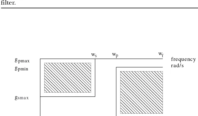
One of the easiest graphical specifications to draw is that for the lowpass
digital filter. From analog filtering the student remembers that a lowpass filter is supposed to pass (or not reduce very much) low frequency signals, while it should stop (or reduce greatly) frequencies above a specified frequency. The band of frequencies specified to be passed by the filter is called the passband, while the range of frequencies specified to be stopped by the filter is called the stopband. As saying this is cumbersome and loaded with ambiguities, almost always a graphical specification is drawn, using the following definitions:
gpmax is the maximum allowed gain in the passband.
gpmin is the minimum allowed gain in the passband.
gsmax is the maximum allowed gain in the stopband.
wp = the highest frequency in the passband
ws = the lowest frequency in the stopband
wf = the folding frequency or half the sampling frequency = π/T in rad/s
Using these definitions, the graphical specification for a lowpass digital filter looks like that in Figure 3.1, where also the frequency axis stops at w = wf, since all DSP system gains will repeat after that, whether you like
it or not.
Example 3.2.
Specification of a digital lowpass filter
Problem: Let’s assume that the customer wants a digital filter that will not amplify the signal at all in the passband while not reducing the gain by more than 3 dB in the passband. The passband extends out to 1,000 rad/s and the stopband starts at 10,000 rad/s. The digital filter is to reduce the gain in the stopband by at least 40 dB. The sampling frequency is given as 40,000 rad/s, or T is 0.16 ms.
Solution: Given these specifications, the graphical specification for the digital lowpass filter is shown in Figure 3.2, with the frequency axis only going out to 20,000 rad/s, since any filter gain will repeat after that.
g
w w w
frequency rad /s g
g gain in dB
p s f
pmax pmin
smax
Figure 3-1. The general lowpass filter graphical specification
frequency rad/s gain
in dB
1,000 10,000 20,000
0 −3
−40
3.3
The Highpass Digital Filter Specification
The highpass filter graphical specification is also not too difficult to draw. A highpass filter is a filter that stops (or greatly reduces) frequencies below a specified frequency, but passes (or changes very little) the frequencies above a specified frequency. The graphical specification for a highpass digital filter can be drawn using the preceding definitions for the lowpass digital filter specification, except that wp is the lowest
frequency in the passband and ws is the highest frequency in the
stopband. This is shown, in general, in Figure 3.3, remembering that there is no need to extend the specification beyond half the sample frequency of wf.
Example 3.3.
Specification of a highpass digital filter
Problem: Let’s assume the customer wants a digital filter running (reads the ADC and outputs to the DAC) at 500 Hz. This is 1,000π rad/s. The filter is required to reduce input frequencies below 200 rad/s by more than 20 dB, but not reduce any input frequencies above 500 rad/s by more than 1 dB and not increase any signals above that.
Solution: The graphical specification for this filter is shown in Figure 3.4. Any filter designed using the methods shown in Chapters 7, 10, and 11 that has a gain in the clear area meets the customer’s specification for the filter.
g w w
w
frequency rad/s g
g
f p
s
smax
pmin pmax
3.4
The Bandpass Digital Filter Specification
The digital bandpass filter specification is a little more complex than the previous two graphical specifications simply because the allowed filter gain region is more complex. A bandpass filter is one that passes (or changes very little) frequencies that are between two specified frequen-cies, while it stops (or greatly reduces) frequencies above and below two other specified frequencies. In order to draw the graphical specifications for a bandpass filter, the following definitions are needed.
gsmax is the maximum allowed gain in the stopbands.
gpmax is the maximum allowed gain in the passband.
gpmin is the minimum allowed gain in the passband.
ws1 is the upper frequency limit of the lower stopband.
wp1 is the lower frequency limit of the passband.
wp2 is the upper frequency limit of the passband.
ws2 is the lower frequency limit of the upper stopband.
wf is half the sampling frequency.
200 500
frequency rad/s gain
0 −1
−20
1,571
in dB
Although this type of filter specification could be made even more complex by specifying different maximum gains for each stop band, this is not usually done. Notice that now there are two stopbands and two transition bands. The general graphical specification for a bandpass digital filter is shown in Figure 3.5. Example 3.4 shows how to draw the bandpass graphical specification.
Example 3.4.
Specification of a bandpass digital filter
Problem: The customer’s requirements are to design a digital filter with the time between samples equal to 0.0005 s. The filter is to reduce all frequencies below 10 Hz and above 500 Hz by more than 60 dB, while not reducing the frequencies between 50 Hz and 100 Hz by more than 2 dB. The filter should also not increase any frequency in the passband by more than 1 dB.
Solution: First the sample time T is used to determine the folding frequency.
wf =
π
T = 6283 rad/s
All the other frequencies are multiplied by 2π to convert to rad/s. Then the graphical specification for the filter is drawn, as in Figure 3.6.
gain in dB
frequency rad/s w
w w
w w
g g
g
p1 p2 s2 f
s1
smax pmin pmax
From Figures 3.3 or 3.4, it can be seen that the graphical specification for a highpass digital filter that is plotted out to the sampling frequency would have the same form as a bandpass filter graphical specification plotted only out to half the sampling frequency. In fact, if the bandpass filter were perfectly symmetrical in frequency (not log of the frequency), it would look exactly like a highpass filter plotted out to its sampling frequency. The only way to be sure is to know what the sampling frequency is and where repetition begins.
3.5
The Bandstop Digital Filter Specification
The bandstop filter is used to stop (or greatly reduce) all frequencies between two specified frequencies, while passing (or reducing very little) frequencies below a specified frequency and above another specified frequency. The definitions given for the bandpass filter can be used for the stopband filter, since the only difference is that now the two stopband frequencies are between the two passband frequencies. Notice that now there is one stopband, two passbands, and two transition bands. Figure 3.7 shows the general stopband filter graphical specification. Again, any filter that we learn to design in later chapters with a gain in the clear region will meet the specification for the filter.
Example 3.5.
Specification of a digital bandstop filter
Problem: The requirements of the filter are that the input signal is sampled at 10,000 rad/s, the frequencies in the input between 1,000
gain in dB
frequency rad/s 3142
314 628
6 3 6283
1 −2
−60
and 2,000 rad/s are to be reduced by at least 40 dB, and the filter is not to increase or decrease frequencies below 500 or above 4,000 rad/s by more than 2 dB.
Solution: The graphical specification for this bandstop digital filter is drawn in Figure 3.8.
The same comment that was made about the relationship of the graphical specifications of highpass and bandpass filters also applies to the relation-ship between bandstop and lowpass digital filter graphical specifications. Because digital filters repeat beyond half the sampling frequency, the graphical specifications for a digital lowpass filter plotted out to its sampling frequency would look like the specifications for a symmetrical
W W W W
frequency rad/s W g
g
g gain in dB
p1 s1 s2 p1 f
pmax
pmin
smax
Figure 3.7. The general bandstop filter specification
500 1,000 2,000
frequency rad/s
gain in dB
5,000 4,000
2 −2
−40
bandstop digital filter. The sampling frequency tells you if the drawing is a repetition of the lowpass filter specification or a bandstop filter.
3.6
Alternate Graphical Specifications
Many digital graphical specifications are drawn with the horizontal axis representing the frequency multiplied by the sample period rather than just the frequency of the gain function. This is just a scaling so that all filters that actually do the same thing with respect to the sampling frequency will look the same, since multiplying by T is dividing by 1/fs,
the sampling frequency in Hz. This new frequency is called the digital or
scaled frequency. It is a fictitious frequency, used only for convenience to specify stop and pass frequencies in terms of fractions of the sampling frequency.
This scaling is helpful in determining the filter coefficients in later chapters. To see what a graphical specification says about the gain at a real frequency, you only need to divide the graph frequency by T. Since the real frequency into or out of a digital filter is multiplied by T, the maximum frequency before the gain repeats at wf is π, as shown in the
following equation.
wf(scaled) = wf(rad/s) * T = 0.5wsT = 0.5(2 π
T)T = π
Thus all graphical specifications when scaled by T go from 0 to π rad/s. The pass and stop frequency specifications also need to be given in terms of the scaled frequency instead of in rad/s. This amounts to multiplying the orig-inal stop and pass frequency specifications by T also. Example 3.6 is just Example 3.5 replotted with the frequency axis scaled by multiplying by T.
Example 3.6.
Graphical specification of a digital stopband filter
using scaled frequency
Problem: The desired digital filter graphical specifications are given by Example 3.5, but the graphical specification is to be drawn using scaled frequencies.
values are multiplied by this number, the new graphical specification is that shown in Figure 3.9, using scaled frequency values on the horizontal axis.
Summary
In Chapter 3 we learned how to draw the graphical specifications of digital filters. The vertical axis is gain, usually in dB, and the horizontal axis is frequency, which is usually scaled logarithmically. The graphical specifi-cations for the four basic types of filters were developed and illustrated. Because digital filters repeated their gain characteristics past the folding frequency (half the sampling frequency), most digital filter plots only go out to that frequency. This does not mean they have no gain out there; it means the gain is a repetition of the lower frequency gain. Also remember that any frequency input to the digital filter above the folding frequency will be added to the corresponding frequency below the folding frequency before the filter works on it.
Finally we defined the scaled frequency, which is the actual input sinusoid frequency of interest multiplied by the sampling period T. By doing this, all graphical specifications and filter gain plots repeat above π rad/s. This is just a fictitious frequency, but it puts all filter specifications relative to the sampling frequency.
Problems
1. Draw the graphical specification of a digital lowpass filter out to the folding frequency in rad/s that will not reduce the gain of
frequen-0.31 0.63 1.25
frequency
gain in dB
3.14 2.5 2
−2
−40
cies below 50 rad/s by more than 2 dB, while reducing the gain of frequencies above 100 rad/s by more than 20 dB. The sampling rate is 500 rad/s.
2. Draw the graphical specification for a digital highpass filter out to the folding frequency in rad/s that will not change the gain above 500 rad/s by more than +/– 3 dB, while reducing the gain below 200 rad/s by more than 40 dB. The sampling time T = 0.001 s.
3. Draw the graphical specification for Problem 2, but use scaled frequencies.
4. Draw the graphical specification for a bandpass digital filter out to its folding frequency that will not reduce the gain between 100 and 200 rad/s by more than 1 dB, but will reduce the gain above 400 rad/s and below 50 rad/s by more than 25 dB. The sampling time T = 0.0005 s. 5. Draw the graphical specification for a stopband digital filter out to its
folding frequency that will reduce the gain between 1,000 rad/s and 5,000 rad/s by more than 60 dB, but will not reduce the gain above 10,000 rad/s or below 150 rad/s by more than 3 dB. The sampling rate is 10,000 Hz.
6. Repeat Problem 5 using scaled frequencies.
7. Draw the graphical specification for a highpass digital filter out to its folding frequency in rad/s that will keep the gain above 500 rad/s between 1 and –3 dB, while reducing the gain below 100 rad/s below 35 dB. The sampling period T = 3.14 ms.
8. Draw the graphical specification for a lowpass digital filter out to its sampling frequency in rad/s that will not reduce the gain more than 4 dB below 250 rad/s, while reducing the gain above 1,000 rad/s by more than 45 dB. The sample period T = 1.57 ms.
9. Draw the graphical specification for Problem 1 out to 500 rad/s. If this were the graphical specification for a sampling rate of 1,000 rad/s, state the type of filter for which it is a graphical specification.
rate of 2 kHz, state the type of filter for which it is a graphical specification.
11. Draw the graphical specification for Problem 4 with the frequency axis scaled in Hz and the sampling time T = 0.001.
12. Draw the graphical specification for Problem 5 with the frequency axis scaled in Hz and the sampling rate is 5,000 Hz.
13. Draw the graphical specification for Problem 1 in terms of loss in dB.
Introduction
We have shown the equation coded for a digital filter in Chapter 1, and in Chapter 2 we showed how to get the discrete or sampled time equation of a signal that is the input or output of a digital filter. However, not all the math representations have been given. In order to analyze or design a digital filter or any other DSP system, an equation of the system itself is required, not just the DSP input-output equation. We get this system equation by using the z-transforms of the sampled signals, just as analog system transfer functions are obtained from the Laplace transforms of signals. The nice thing about understanding and obtaining z-transforms is that it involves only algebra, whereas Laplace transforms involve integration from calculus.
4.1
The Need for z-Transforms of the DSP Equation
This chapter defines and shows how to ob tain the z-transforms of any sampled signal. As some of the results of taking the z-transforms of specific sampled time signals are listed in Table 4.1, the z-transforms of many signals will have to be computed only once. Then, just as for Laplace transforms, a transfer function will be obtained in Chapter 5 using the ratio of the output over the input signals of the DSP system (both signals are z-transformed). This is a necessary evil to get the mathematical description of the sampled system. The transfer function must be the
z-Transforms
c h a p t e r
system description, since by the preceding definition, if you multiply it by the z-transform of any input signal, you get the z-transform of the output signal as shown hereafter, with capitals representing the z-transforms of the signals.
Y(z)= Y(z)
X(z)X(z)=T(z)X(z)
In the equation ab ove, x(t) is the input into the ADC and y(t) is the output from the DAC and T(z) must be the DSP system description, since if you multiply it by the z-transform of the input, you get the z-transform of the output.
The reason for using z-transforms is that the preceding equation is valid. If you took the ratio of sampled output signal to sampled input signal to a DSP system, you would get some expression, but it would change for each input signal. By using the z-transforms of the signals, the ratio of any output to the corresponding input is always the same expression and must be the system math description, since when it is multiplied by the input, you get the output. With a math description of a digital filter, it is then possible to analyze its characteristics and even design a filter to meet the desired graphical specifications shown in Chapter 3.
4.2
The Definition of the z-Transform and Its Use
The definition of the z-transform of a sampled signal f(n) is F(z), as defined by Equation 4.1.
F(z)=
∑
n=−∞∞
f(n)z−n=Z[f(n)]=⋅⋅⋅+f(−1)z1+f(0)+f(a)z−1
+f(2)z2⋅⋅⋅
(Equation 4.1)
Example 4.1.
The z-transform of a signal with only a few sample
values
Problem: Let the input signal f(t) into an ADC be 2t for t greater than zero and less than 4, and zero otherwise. Let’s find the z-transform of this short signal when T = 1.
Solution: The sample times occur at integer values of t, and the only nonzero output samples of the ADC will be f(1) = 2, f(2) = 4, f(3) = 6. Using the definition for the z-transform of a signal in Equation 4.1, it is seen that the z-transform of the signal is given by the following equation.
F(z)= 2z−1+ 4z−2+ 6z−3
In order to determine the z-transforms of more complex signals and those that never end, we need to define two basic sampled signals and obtain their z-transforms. The first is a sampled signal that consists of just one sample, this is called the impulse or δ function. It is defined mathemati-cally in the following equations, and as can be seen, it is not the δ function or impulse function used for continuous signals since it has a finite amplitude of 1.
δ(nt) = δ(n) = 0, n≠ 0
δ(0) = 1
The other basic sampled signal that needs to be defined is the sampled unit step function u(n), as given in the following equation.
u(nT) = u(n) = 1, n ≥ 0
Notice again the shorthand notation of replacing the argument in each function by n, since it is understood that u(n) occurs at t = nT.
It is easily shown in the following equations that the z-transform of the impulse function is Z[δ(n)] = 1, since δ(0) = 1 and all other sample values are 0.
Z[δ(n)] =⋅⋅⋅+δ(−1)z1+δ(0)z0+δ(1)z−1+⋅⋅⋅
= 1z0
Also the z-transform of an impulse function shifted by t = kT, where k is an integer, is easy to obtain, as shown in the following equation.
Z[δ(n−k)] =⋅⋅⋅+δ(−1)z1−k+δ(n−k)z−k+δ(1)z−k−1+⋅⋅⋅=z−k
The preceding result is obtained since the impulse function is zero everywhere the argument is not zero.
The z-transform of the impulse allows the discrete time equation of a few samples to be written mathematically and then the z-transform can be taken, as shown in Example 4.2, or the discrete time equation can easily be written from the z-transform.
Example 4.2.
Using the impulse function for short sampled signal
description
Problem: Use the impulse function to describe a sampled signal where the initial sample x(0) = 2, x(3) = –2, and the rest of the samples are zero.
Solution: Using the shifting property of time signals and the fact that a sum of two time-shifted impulse functions doesn’t add at the correspond-ing times when they are nonzero, we get
x(n) = 2δ(n) – 2δ(n – 3)
X(z) = 2 – 2z–2
The z-transform of the unit step, u(n), is more difficult to obtain in a closed form, but the procedure only involves a little algebra, which is shown in the following equations.
Z[u(n)] +U(z)= 1 +z−1+ 1z−2+ 1z−3+⋅⋅⋅
This summation starts at f(0) = u(0) =1 and goes on forever. However, if we multiply U(z) by z–1 we get
z−1U(z)= 1z−1+ 1z−2+⋅⋅⋅
If we subtract the second equation from the first equation, we get the following equations.
U(z)[1 −z−1] = 1
Now dividing both sides by the term in the brackets, we get the final z-transform of u(n):
U(z)= 1 1 −z−1 =
z z− 1
As can be seen, U(z), the z-transform of u(nT) = u(n), is not very complicated. One of the major uses of the sampled unit step is to start and stop a signal. This is shown in one of the problems at the end of the chapter.
4.3
Derivation of the Necessary z-Transform Pairs
In the preceding section, we determined the z-transforms of two basic sampled signals, the unit impulse and the sampled unit step. In this section we expand on the pairs of sampled signals and the corresponding z-transform, using basic algebra. It is useful also to relate the sampled signal coming out of an ADC to the analog signal coming in, which is shown in column 1 of Table 4.1.
The definition of the z-transform of a sampled signal shows that if any sampled signal is A times bigger, then its z-transform is A times bigger, as shown in the following equation.
Z[A f(n)] =⋅⋅⋅+A f(−1)z1+A f(0)+A f(1)z−1+⋅⋅⋅
=A[⋅⋅⋅+f(−1)z1+f(0)+f(1)z−1+⋅⋅⋅] =A Z[f(n)]
Using the property just defined, we already can say
Z[Aδ(n)] = A
and
Z[A u(n)] = A z
z− 1
Another very useful and common analog signal is the exponential decaying signal that starts at t = 0. This signal and its sampled equation are given in the following equations.
f(t) = A e–at u(t)
f(nT) = f(n) = A e–anTu(n)
= A(e-aT)n = A cn, c = e–aT = a constant
Analog Signal Sampled Signal Z-transformed Signal
Aδ(n) A
Au(t) Au(n) Az
z−1
Ae-at
u(t) Ae−aTn
u(n) Az
z−e−aT
Acn u(n) Az , c = e−aT
z−c
Atu(t) AnTu(n) ATz
(z−1)2
Acos(wt)u(t) Acos(wTn)u(n) Az[z−cos(wT)] z2−2zcos(wT) +1
Asin(wt)u(t) Asin(wTn)u(n) Azsin(wT) z2−2zsin(wT) +1
Ae−at
cos(wt + α)u(t) Acn
cos(wTn + α) Az[z cos(α) −c cos(α −wT)] z2−2cz cos(wT) +c2 −
Table 4.1
Now using the definition of a z-transform and the z-transform of a step of
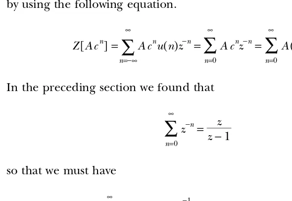
A, we can get the z-transform of a sampled exponentially decaying signal by using the following equation.
Z[Acn] =
∑
n=−∞∞
A cnu(n)z−n=
∑
n=0∞
A cnz−n=
∑
n=0∞
A(c−1z)−n
In the preceding section we found that
∑
n=0
∞
z−n= z
z− 1
so that we must have
∑
n=0
∞
(c−1z)−n= c
−1
z c−1z− 1=
z z−c =
z z−e−aT
Thus the z-transform of a sampled exponential decaying signal that starts at t = 0 is
Z[A e−anT] = Az
z−c, where c = e
–aT.
The z-transform just given is one of the most important in DSP. Later it will be used to determine the stability and other properties of any DSP system.
Tab le 4.1 lists the z-transform pairs that we have obtained so far, along with some others. The mathematical derivation of some of these is done the same way as that for the exponentially decaying sampled signal, but the final closed form solution requires the use of the Euler equation, which is not given until Chapter 6. The organization of Table 4.1 is that the analog signal is given in column 1, the sampled version of the analog signal is given in column 2, and the z-transform of the sampled signal in column 2 is given in column 3. Note that the time signals are zero before
starting at t = 0. The z-transform of the product of two signals is not the product of the z-transforms. Example 4.3 illustrates the use of Table 4.1.
Example 4.3.
Using Table 4.1 to get the z-transforms of signals
Problem: Let the input signal to an ADC be given below with T = 0.5 s.
x(t)= 7e−3tu(t)
Solution: For the preceding signal, we can see that A = 7, a = 3. Thus the sampled signal and the z-transform of the sampled signal are given in the following equations.
x(n)= 7e−1.5nu(n)
X(z)= 7z
z− e−1.5
4.4
Derivation of the Major z-Transform Property Using Algebra
Using basic algebra we will use the definition of the z-transform to derive the major property of z-transforms. Later this property will allow the student to go back and forth between the DSP system math description
T(z) in terms of the variab le z and the difference equation given in Chapter 1, which is the equation that is actually coded. This property will be developed in two different ways for the student. This property is called the shifting property, and it relates the z-transform of sampled signals that are time-shifted versions of each other if the time shift is in integer multiples of the sample time T. Remember that any signal or function of time that is delayed by kT is written in terms of the unshifted signal f(nT) as f(nT – kT), or f(n – k). After the first method of derivation of this property, examples using it will be given.
Z[f(n−k)] =
∑
n=−∞∞
f(n−k)z−n
If we let u = n – k in the expression on the right, we have
Z[f(n−k)] =
∑
n=−∞∞
f(u)z−(u+k)=
∑
u=−∞∞
f(u)z−uz−k=z−k
∑
u=−∞ ∞
f(u)z−u=z−kF(z)
Where we have used n = u + k and in the definition z can be replaced by
u without any effect (it is a symbol used as a placeholder). The significance of the preceding equation (called the shifting property) is that if the differenc e equation for a digital filter is given, the use of this property on the equation gives an algebraic equation for the digital filter. Another significant property is shown in later chapters when we design a digital filter or DSP system, which is mathematically expressed in terms of the variable z, we can use the property to get the difference equation to code in a computer or a DSP chip. Let’s look at a few examples of using this property on a sampled signal. In the next chapter this property is used on the DSP difference equation to obtain the math description of the DSP system.
Example 4.4.
Writing the z-transform of the sampled signal
f
(
n
)
delayed by 3 sample periods
Problem: Let f(n) = f(nT) be an arbitrary sampled signal. We want to write the equation for this signal if it is delayed in time by 3T.
Solution: The delayed signal is written mathematically as f(nT – 3T) or
f(n – 3), where k = 3. A direct application of the preceding property gives the following answer, where F(z) is the z-transform of f(n).
f(n – 3) = z–3F(z)
Example 4.5.
Writing the z-transform of an equation with shifted
functions
Problem: Write the z-transform of the following equation of a DSP system.
Solution: Taking the z-transform of all the signals in the equation, we get the following equation.
Y(z)= 2z−1Y(z)+ 0.5z−1X(z)
The significance of this property of the z-transform of a signal is its use on the equation of a DSP system, as in Example 4.5, especially the digital filter equation given in Chapter 1. Remember it is composed of current and delayed inputs and delayed outputs. This kind of equation is called a difference equation, and it is the discrete-time equivalent to the analog differential equation. In Chapter 5 we will see that this property of th