Coplanar Waveguide
Circuits,
Components, and
Systems
Coplanar Waveguide
Circuits,
Components, and
Systems
RAINEE N. SIMONS NASA Glenn Research Center Cleveland, Ohio
A JOHN WILEY & SONS, INC., PUBLICATION
Designations used by companies to distinguish their products are often claimed as trademarks. In all instances where John Wiley & Sons, Inc., is aware of a claim, the product names appear in initial capital or . Readers, however, should contact the appropriate companies for more complete information regarding trademarks and registration. Copyright2001 by John Wiley & Sons. All rights reserved.
No part of this publication may be reproduced, stored in a retrieval system or transmitted in any form or by any means, electronic or mechanical, including uploading, downloading, printing, decompiling, recording or otherwise, except as permitted under Sections 107 or 108 of the 1976 United States Copyright Act, without the prior written permission of the Publisher. Requests to the Publisher for permission should be addressed to the Permissions Department, John Wiley & Sons, Inc., 605 Third Avenue, New York, NY 10158-0012,(212)850-6011, fax(212) 850-6008, E-Mail: PERMREQWILEY.COM.
This publication is designed to provide accurate and authoritative information in regard to the subject matter covered. It is sold with the understanding that the publisher is not engaged in rendering professional services. If professional advice or other expert assistance is required, the services of a competent professional person should be sought.
ISBN 0-471-22475-8
This title is also available in print as ISBN 0-471-16121-7.
Joy, Renita, and
CHAPTER
Contents
Preface ix
1 Introduction 1
1.1 Advantages of Coplanar Waveguide Circuits 1
1.1.1 Design 1
1.1.2 Manufacturing 2
1.1.3 Performance 2
1.2 Types of Coplanar Waveguides 3
1.3 Software Tools for Coplanar Waveguide Circuit Simulation 4 1.4Typical Applications of Coplanar Waveguides 4
1.4.1 Amplifiers, Active Combiners, Frequency Doublers,
Mixers, and Switches 4
1.4.2 Microelectromechanical Systems(MEMS)Metal
Membrane Capacitive Switches 4
1.4.3 Thin Film High-Temperature Superconducting/
Ferroelectric Tunable Circuits and Components 5
1.4.4 Photonic Bandgap Structures 5
1.4.5 Printed Antennas 5
1.5 Organization of This Book 6
References 7
2 Conventional Coplanar Waveguide 11
2.1 Introduction 11
2.2 Conventional Coplanar Waveguide on a Multilayer
Dielectric Substrate 12
2.2.1 Analytical Expression Based on Quasi-static Conformal Mapping Techniques to Determine Effective Dielectric Constant and Characteristic
Impedance 12
2.2.2 Conventional Coplanar Waveguide on an Infinitely
Thick Dielectric Substrate 17
2.2.3 Conventional Coplanar Waveguide on a Dielectric
Substrate of Finite Thickness 20
2.2.4Conventional Coplanar Waveguide on a Finite Thickness Dielectric Substrate and with a Top
Metal Cover 21
2.2.5 Conventional Coplanar Waveguide Sandwiched
between Two Dielectric Substrates 24
2.2.6 Conventional Coplanar Waveguide on a
Double-Layer Dielectric Substrate 25
2.2.7 Experimental Validation 29
2.3 Quasi-static TEM Iterative Techniques to Determine andZ
32
2.3.1 Relaxation Method 32
2.3.2 Hybrid Method 33
2.4Frequency-Dependent Techniques for Dispersion and
Characteristic Impedance 33
2.4.1 Spectral Domain Method 33
2.4.2 Experimental Validation 44
2.5 Empirical Formula to Determine Dispersion Based on
Spectral Domain Results 47
2.5.1 Comparison of Coplanar Waveguide Dispersion
with Microstrip 48
2.6 Synthesis Formulas to Determine
andZBased on
Quasi-static Equations 49
2.7 Coplanar Waveguide with Elevated or Buried Center
Strip Conductor 52
2.7.1 CPW with Elevated Center Strip Conductor
Supported on Dielectric Layers 54
2.7.2 CPW with Elevated Center Strip Conductor
Supported on Posts 54
2.8 Coplanar Waveguide with Ground Plane or Center Strip
Conductor Underpasses 56
2.10 Coplanar Waveguide on a Cylindrical Surface 63 2.10.1 Analytical Expressions Based on Quasi-static
Conformal Mapping Technique 63
2.10.2 Computed Effective Dielectric Constant and
Characteristic Impedance 67
2.11 Effect of Metalization Thickness on Coplanar Waveguide
Characteristics 67
Appendix 2A: Spectral Domain Dyadic Green’s Function
Components 69
Appendix 2B: Time Average Power Flow in the Three Spatial
Regions 77
References 83
3 Conductor-Backed Coplanar Waveguide 87
3.1 Introduction 87
3.2 Conductor-Backed Coplanar Waveguide on a Dielectric
Substrate of Finite Thickness 88
3.2.1 Analytical Expressions Based on Quasi-static TEM Conformal Mapping Technique to Determine Effective Dielectric Constant and Characteristic
Impedance 88
3.2.2 Experimental Validation 89
3.2.3 Analytical Expressions for CBCPW
andZ
in the Presence of a Top Metal Cover 93 3.2.4Dispersion and Characteristic Impedance from
Full-Wave Analysis 96
3.3 Effect of Conducting Lateral Walls on the Dominant Mode Propagation Characteristics of CBCPW and Closed Form Equations forZ
98
3.3.1 Experimental Validation 101
3.4Effect of Lateral Walls on the Higher-Order Mode
Propagation on CBCPW 102
3.4.1 Perfect Conductors and Lossless Dielectric 102 3.4.2 Conductors with Finite Thickness, Finite
Conductivity, and Lossless or Lossy Dielectric 104
3.4.3 Experimental Validation 107
3.5 Channelized Coplanar Waveguide 107
3.6 Realization of Lateral Walls in Practical Circuits 108
References 109
4 Coplanar Waveguide with Finite-Width Ground Planes 112
4.1 Introduction 112
4.2 Conventional Coplanar Waveguide with Finite-Width Ground Planes on a Dielectric Substrate of
Finite Thickness 113
4.2.1 Analytical Expressions Based on Quasi-static TEM Conformal Mapping Techniques to Determine Effective Dielectric Constant and
Characteristic Impedance 113
4.2.2 Dispersion and Characteristic Impedance from
Full-Wave Analysis 117
4.3 Conductor-Backed Coplanar Waveguide with Finite-Width Ground Planes on a Dielectric Substrate of
Finite Thickness and Finite Width 119
4.4 Simple Models to Estimate Finite Ground Plane
Resonance in Conductor-Backed Coplanar Waveguide 123
4.4.1 Experimental Validation 124
References 125
5 Coplanar Waveguide Suspended inside a Conducting Enclosure 127
5.1 Introduction 127
5.2 Quasi-static TEM Iterative Technique to Determine andZ
of Suspended CPW 128
5.2.1 Computed Quasi-static Characteristics and
Experimental Validation 128
5.3 Frequency-Dependent Numerical Techniques for Dispersion
and Characteristic Impedance of Suspended CPW 132 5.3.1 Effect of Shielding on the Dispersion and
Characteristic Impedance 133
5.3.2 Experimental Validation of Dispersion 135 5.3.3 Effect of Conductor Thickness on the Dispersion
and Characteristic Impedance 135
5.3.4Modal Bandwidth of a Suspended CPW 136 5.3.5 Pulse Propagation on a Suspended CPW 140 5.3.6 Pulse Distortion—Experimental Validation 142 5.4Dispersion and Higher-Order Modes of a Shielded
Grounded CPW 142
Modes of a CPW Suspended inside a Nonsymmetrical
Shielding Enclosure 143
5.5.1 Experimental Validation of the Dispersion
Characteristics 146
5.6 Dispersion and Characteristic Impedance of Suspended
CPW on Multilayer Dielectric Substrate 147
References 150
6 Coplanar Striplines 152
6.1 Introduction 152
6.2 Analytical Expressions Based on Quasi-Static TEM Conformal Mapping Techniques to Determine Effective
Dielectric Constant and Characteristic Impedance 153 6.2.1 Coplanar Stripline on a Multilayer Dielectric Substrate 153 6.2.2 Coplanar Stripline on a Dielectric Substrate of Finite
Thickness 155
6.2.3 Asymmetric Coplanar Stripline on a Dielectric
Substrate of Finite Thickness 157
6.2.4Coplanar Stripline with Infinitely Wide Ground Plane
on a Dielectric Substrate of Finite Thickness 160 6.2.5 Coplanar Stripline with Isolating Ground Planes on a
Dielectric Substrate of Finite Thickness 161 6.3 Coplanar Stripline Synthesis Formulas to Determine the
Slot Width and the Strip Conductor Width 162 6.4Novel Variants of the Coplanar Stripline 164
6.4.1 Micro-coplanar Stripline 164
6.4.2 Coplanar Stripline with a Groove 164
References 169
7 Microshield Lines and Coupled Coplanar Waveguide 171
7.1 Introduction 171
7.2 Microshield Lines 171
7.2.1 Rectangular Shaped Microshield Line 173
7.2.2 V-Shaped Microshield Line 176
7.2.3 Elliptic Shaped Microshield Line 180
7.2.4Circular Shaped Microshield Line 180
7.3 Edge Coupled Coplanar Waveguide without a Lower
Ground Plane 182
7.3.1 Even Mode 182
7.3.2 Odd Mode 186
7.3.3 Computed Even- and Odd-Mode Characteristic
Impedance and Coupling Coefficient 189
7.4Conductor-Backed Edge Coupled Coplanar Waveguide 190
7.4.1 Even Mode 192
7.4.2 Odd Mode 192
7.4.3 Even- and Odd-Mode Characteristics with Elevated
Strip Conductors 193
7.5 Broadside Coupled Coplanar Waveguide 193
7.5.1 Even Mode 194
7.5.2 Odd Mode 197
7.5.3 Computed Even- and Odd-Mode Effective Dielectric Constant, Characteristic Impedance, Coupling
Coefficient, and Mode Velocity Ratio 198
References 201
8 Attenuation Characteristics of Conventional,
Micromachined, and Superconducting Coplanar Waveguides 203
8.1 Introduction 203
8.2 Closed Form Equations for Conventional CPW Attenuation
Constant 204
8.2.1 Conformal Mapping Method 205
8.2.2 Mode-Matching Method and Quasi-TEM Model 207 8.2.3 Matched Asymptotic Technique and Closed Form
Expressions 207
8.2.4Measurement-Based Design Equations 212 8.2.5 Accuracy of Closed Form Equations 215 8.3 Influence of Geometry on Coplanar Waveguide Attenuation 217
8.3.1 Attenuation Constant Independent of the Substrate
Thickness and Dielectric Constant 217
8.3.2 Attenuation Constant Dependent on the Aspect Ratio 217 8.3.3 Attenuation Constant Varying with the Elevation of
the Center Strip Conductor 218
8.4Attenuation Characteristics of Coplanar Waveguide on
Silicon Wafer 218
8.4.1 High-Resistivity Silicon Wafer 218
8.5 Attenuation Characteristics of Coplanar Waveguide on
Micromachined Silicon Wafer 221
8.5.1 Microshield Line 221
8.5.2 Coplanar Waveguide withV-Shaped Grooves 223 8.5.3 Coplanar Waveguide Suspended by a Silicon Dioxide
Membrane over a Micromachined Wafer 223 8.6 Attenuation Constant for Superconducting Coplanar
Waveguides 225
8.6.1 Stopping Distance 225
8.6.2 Closed Form Equations 230
8.6.3 Comparison with Numerical Calculations and
Measured Results 233
References 233
9 Coplanar Waveguide Discontinuities and Circuit Elements 237
9.1 Introduction 237
9.2 Coplanar Waveguide Open Circuit 237
9.2.1 Approximate Formula for Length Extension When
the Gap Is Large 239
9.2.2 Closed Form Equation for Open End Capacitance
When the Gap Is Narrow 239
9.2.3 Radiation Loss 240
9.2.4Effect of Conductor Thickness and Edge Profile Angle 241
9.3 Coplanar Waveguide Short Circuit 241
9.3.1 Approximate Formula for Length Extension 241 9.3.2 Closed Form Equations for Short-Circuit Inductance 242 9.3.3 Effect of Conductor Thickness and Edge Profile Angle 243
9.4Coplanar Waveguide MIM Short Circuit 243
9.5 Series Gap in the Center Strip Conductor of a Coplanar
Waveguide 245
9.6 Step Change in the Width of Center Strip Conductor of a
Coplanar Waveguide 245
9.7 Coplanar Waveguide Right Angle Bend 247
9.8 Air-Bridges in Coplanar Waveguide 249
9.8.1 Type A Air-Bridge 250
9.8.2 Type B Air-Bridge 250
9.8.3 Air-Bridge Characteristics 250
9.8.4Air-Bridge Discontinuity Characteristics 254
9.9 Coplanar WaveguideT-Junction 254
9.9.1 ConventionalT-Junction 254
9.9.2 Air-BridgeT-Junction 259
9.9.3 Mode Conversion in CPWT-Junction 260
9.9.4CPWT-Junction Characteristics 261
9.10 Coplanar Waveguide Spiral Inductor 262
9.11 Coplanar Waveguide Capacitors 265
9.11.1 Interdigital Capacitor 266
9.11.2 Series Metal-Insulator-Metal Capacitor 269 9.11.3 Parallel Metal-Insulator-Metal Capacitor 270 9.11.4Comparison between Coplanar Waveguide
Interdigital and Metal-Insulator-Metal
Capacitors 271
9.12 Coplanar Waveguide Stubs 272
9.12.1 Open-End Coplanar Waveguide Series Stub 273 9.12.2 Short-End Coplanar Waveguide Series Stub 275 9.12.3 Combined Short- and Open End Coplanar
Waveguide Series Stubs 278
9.12.4Coplanar Waveguide Shunt Stubs 278
9.12.5 Coplanar Waveguide Radial Line Stub 278
9.13 Coplanar Waveguide Shunt Inductor 282
References 285
10 Coplanar Waveguide Transitions 288
10.1 Introduction 288
10.2 Coplanar Waveguide-to-Microstrip Transition 289 10.2.1 Coplanar Waveguide-to-Microstrip Transition
Using Ribbon Bond 289
10.2.2 Coplanar Waveguide-to-Microstrip
Surface-to-Surface Transition via Electromagnetic
Coupling 290
10.2.3 Coplanar Waveguide-to-Microstrip Transition via
a Phase-Shifting Network 292
10.2.4Coplanar Waveguide-to-Microstrip Transition via
a Metal Post 292
10.2.5 Coplanar Waveguide-to-Microstrip Transition
10.2.6 Coplanar Waveguide-to-Microstrip Orthogonal
Transition via Direct Connection 296
10.3 Transitions for Coplanar Waveguide Wafer probes 298 10.3.1 Coplanar Waveguide Wafer Probe-to-Microstrip
Transitions Using a Radial Stub 298
10.3.2 Coplanar Waveguide Wafer Probe-to-Microstrip
Transition Using Metal Vias 299
10.4Transitions between Coplanar Waveguides 300 10.4.1 Grounded Coplanar Waveguide-to-Microshield
Coplanar Line 300
10.4.2 Vertical Fed-through Interconnect between Coplanar Waveguides with Finite-Width
Ground Planes 301
10.4.3 Orthogonal Transition between Coplanar
Waveguides 302
10.4.4 Electromagnetically Coupled Transition between
Stacked Coplanar Waveguides 303
10.4.5 Electromagnetically Coupled Transition between
Orthogonal Coplanar Waveguides 304
10.5 Coplanar Waveguide-to-Rectangular Waveguide
Transition 306
10.5.1 Coplanar Waveguide-to-Ridge Waveguide In-line
Transition 306
10.5.2 Coplanar Waveguide-to-Trough Waveguide
Transition 308
10.5.3 Coplanar Waveguide-to-Rectangular Waveguide
Transition with a Tapered Ridge 313
10.5.4Coplanar Waveguide-to-Rectangular Waveguide
End Launcher 314
10.5.5 Coplanar Waveguide-to-Rectangular Waveguide
Launcher with a Post 315
10.5.6 Channelized Coplanar Waveguide-to-Rectangular
Waveguide Launcher with an Aperture 317 10.5.7 Coplanar Waveguide-to-Rectangular Waveguide
Transition with a Printed Probe 318
10.6 Coplanar Waveguide-to-Slotline Transition 318 10.6.1 Coplanar Waveguide-to-Slotline Compensated
Marchand Balun or Transition 319
10.6.2 Coplanar Waveguide-to-Slotline Transition with
10.6.3 Coplanar Waveguide-to-Slotline Double-Y Balun
or Transition 323
10.6.4Electromagnetically Coupled Finite-Width Coplanar Waveguide-to-Slotline Transition with
Notches in the Ground Plane 327
10.6.5 Electromagnetically Coupled Finite-Width Coplanar Waveguide-to-Slotline Transition with
Extended Center Strip Conductor 328
10.6.6 Air-Bridge Coupled Coplanar
Waveguide-to-Slotline Transition 329
10.7 Coplanar Waveguide-to-Coplanar Stripline Transition 331 10.7.1 Coplanar Stripline-to-Coplanar Waveguide Balun 331 10.7.2 Coplanar Stripline-to-Coplanar Waveguide Balun
with Slotline Radial Stub 332
10.7.3 Coplanar Stripline-to-Coplanar Waveguide
Double-Y Balun 333
10.8 Coplanar Stripline-to-Microstrip Transition 334 10.8.1 Coplanar Stripline-to-Microstrip Transition with
an Electromagnetically Coupled Radial Stub 334 10.8.2 Uniplanar Coplanar Stripline-to-Microstrip
Transition 336
10.8.3 Coplanar Stripline-to-Microstrip Transition 337 10.8.4Micro-coplanar Stripline-to-Microstrip Transition 338 10.9 Coplanar Stripline-to-Slotline Transition 339 10.10 Coplanar Waveguide-to-Balanced Stripline Transition 342
References 342
11 Directional Couplers, Hybrids, and Magic-Ts 346
11.1 Introduction 346
11.2 Coupled-Line Directional Couplers 346
11.2.1 Edge Coupled CPW Directional Couplers 349 11.2.2 Edge Coupled Grounded CPW Directional
Couplers 350
11.2.3 Broadside Coupled CPW Directional Coupler 351
11.3 Quadrature(90°)Hybrid 352
11.3.4Reduced Size Impedance Transforming Branch-Line
Hybrid 358
11.4180° Hybrid 361
11.4.1 Standard 180° Ring Hybrid 363
11.4.2 Size Reduction Procedure for 180° Ring Hybrid 364
11.4.3 Reduced Size 180° Ring Hybrid 364
11.4.4 Reverse-Phase 180° Ring Hybrid 368
11.4.5 Reduced Size Reverse-Phase 180° Ring Hybrid 369
11.5 Standard 3-dB Magic-T 371
11.5.1 Reduced Size 3-dB Magic-T 375
11.6 Active Magic-T 378
References 383
12 Coplanar Waveguide Applications 384
12.1 Introduction 384
12.2 MEMS Coplanar Waveguide Capacitive Metal Membrane
Shunt Switch 384
12.2.1 OFF and ON Capacitances 384
12.2.2 Figure of Merit 386
12.2.3 Pull Down Voltage 387
12.2.4Fabrication Process 389
12.2.5 Switching Time and Switching Energy 391
12.2.6 Insertion Loss and Isolation 391
12.3 MEMS Coplanar Waveguide Distributed Phase Shifter 393
12.3.1 MEMS Air-Bridge Capacitance 395
12.3.2 Fabrication and Measured Performance 397 12.4High-Temperature Superconducting Coplanar Waveguide
Circuits 398
12.4.1 High-Frequency Electrical Properties of Normal
Metal Films 398
12.4.2 High-Frequency Electrical Properties of Epitaxial High-T
Superconducting Films 399
12.4.3 Kinetic and External Inductances of a
Superconducting Coplanar Waveguide 401 12.4.4 Resonant Frequency and Unloaded Quality Factor 402 12.4.5 Surface Resistance of High-T
Superconducting
Coplanar Waveguide 407
12.4.6 Attenuation Constant 409 12.5 Ferroelectric Coplanar Waveguide Circuits 410
12.5.1 Characteristics of Barium Strontium Titanate Thin
Films 410
12.5.2 Characteristics of Strontium Titanate Thin Films 413 12.5.3 Grounded Coplanar Waveguide Phase Shifter 414
12.6 Coplanar Photonic-Bandgap Structure 417
12.6.1 Nonleaky Conductor-Backed Coplanar Waveguide 417
12.7 Coplanar Waveguide Patch Antennas 422
12.7.1 Grounded Coplanar Waveguide Patch Antenna 422 12.7.2 Patch Antenna with Electromagnetically Coupled
Coplanar Waveguide Feed 424
12.7.3 Coplanar Waveguide Aperture-Coupled Patch
Antenna 425
References 430
CHAPTER
Preface
This book is intended to provide a comprehensive coverage of the analysis and applications of coplanar waveguides to microwave circuits and antennas for graduate students in electrical engineering and for practicing engineers.
Coplanar waveguides are a type of planar transmission line used in microwave integrated circuits (MICs) as well as in monolithic microwave integrated circuits (MMICs). The unique feature of this transmission line is that it is uniplanar in construction, which implies that all of the conductors are on the same side of the substrate. This attribute simplifies manufacturing and allows fast and inexpensive characterization using on-wafer techniques.
The first few chapters of the book are devoted to the determination of the propagation parameters of conventional coplanar waveguides and their vari-ants. The remaining chapters are devoted to discontinuities and circuit el-ements, transitions to other transmission media, directional couplers, hybrids and magic-T, microelectromechanical systems (MEMS) based switches and phase shifters, high-T
superconducting circuits, tunable devices using ferroelec-tric materials, photonic bandgap structures, and printed circuit antennas. The author includes several valuable details such as the derivation of the fundamen-tal equations, physical explanations, and numerical examples.
The book is an outgrowth of 15 years of research conducted by the author as a member of the Communications Technology Division (CTD) at the National Aeronautics and Space Administration (NASA), Glenn Research Center (GRC) in Cleveland, Ohio. Over the past few years, interest among engineers in coplanar waveguides has increased tremendously, with some of the concepts being extensively pursued by NASA for future space programs and missions. Numerous articles exist, but there is no collective publication. Thus the decision to publish a book on coplanar waveguides appears to be appropriate.
In the course of writing this book, several persons have assisted the author and offered support. The author first expresses his appreciation to the manage-ment of CTD at GRC for providing the environmanage-ment in which he worked on
the book; without their support this book could not have materialized. In particular, he is grateful to Wallace D. Williams, Regis F. Leonard and Charles A. Raquet. The author is further grateful to the engineers and scientists in CTD who shared their time, knowledge, and understanding of this subject. In particular, he would like to thank Samuel A. Alterovitz, Alan N. Downey, Fred Van Keuls, Felix A. Miranda, George E. Ponchak, Maximillian Scardelletti, Joseph D. Warner, Richard R. Kunath, Richard Q. Lee, Hung D. Nguyen, Robert R. Romanofsky, Kurt A. Shalkhauser, and Afroz J. Zaman. In addition the author is grateful to the staff of the clean room and the hybrid/printed circuit fabrication facilities. In particular, he is thankful to William M. Furfaro, Elizabeth A. Mcquaid, Nicholas C. Varaljay, Bruce J. Viergutz and George W. Readus.
The author is grateful to the staff of Publishing Services at GRC for their efficiency in the preparation of the text and illustrations. In particular, he is grateful to Caroline A. Rist, Catherine Gordish, Irene Gorze, and Patricia A. Webb of the co-ordination section, Denise A. Easter and Theresa Young of the manuscript section, and Richard J. Czentorycki, Mary M. Eitel, John L. Jindra, and Nancy C. Mieczkowski of the graphical illustration section. The author is also grateful to the Library at GRC for the help in the literature search.
The author gratefully acknowledges the support and the interactions he has had with Prof. L. P. B. Katehi, Prof. G. M. Rebeiz, Dr. J. R. East, and their students at the University of Michigan, Ann Arbor, for over a decade.
The author thanks Prof. Kai Chang of Texas A&M University, College Station, who suggested and encouraged the writing of this book, and the editorial staff of John Wiley & Sons for the processing of the manuscript.
Finally, the author thanks his wife, Joy, and daughters, Renita and Rona, for their patience during the writing of this book.
RAINEEN. SIMONS
CHAPTER 1
Introduction
A coplanar waveguide (CPW) fabricated on a dielectric substrate was first demonstrated by C. P. Wen [1] in 1969. Since that time, tremendous progress has been made in CPW based microwave integrated circuits(MICs)as well as monolithic microwave integrated circuits(MMICs)[2] to [5].
1.1 ADVANTAGES OF COPLANAR WAVEGUIDE CIRCUITS
1.1.1 Design
A conventional CPW on a dielectric substrate consists of a center strip conductor with semi-infinite ground planes on either side as shown in Figure 1.1. This structure supports a quasi-TEM mode of propagation. The CPW offers several advantages over conventional microstrip line: First, it simplifies fabrication: second, it facilitates easy shunt as well as series surface mounting of active and passive devices [6] to [10]; third, it eliminates the need for wraparound and via holes [6] and [11], and fourth, it reduces radiation loss [6]. Furthermore the characteristic impedance is determined by the ratio of a/b, so size reduction is possible without limit, the only penalty being higher losses [12]. In addition a ground plane exists between any two adjacent lines, hence cross talk effects between adjacent lines are very week [6]. As a result, CPW circuits can be made denser than conventional microstrip circuits. These, as well as several other advantages, make CPW ideally suited for MIC as well as MMIC applications.
1.1.2 Manufacturing
Major advantages gained in manufacturing are, first, CPW lends itself to the use of automatic pick-and-place and bond assembly equipments for surface-mount component placement and interconnection of components, respectively
1
FIGURE 1.1 Schematic of a coplanar waveguide (CPW) on a dielectric substrate of finite thickness.
[6]. Second, CPW allows the use of computer controlled on-wafer measure-ment techniques for device and circuit characterization up to several tens of GHz [13], [14]. These advantages make CPW based MICs and MMICs cost effective in large volume.
1.1.3 Performance
The quasi-TEM mode of propagation on a CPW has low dispersion and hence offers the potential to construct wide band circuits and components. In CPW amplifier circuits, by eliminating via holes and its associated parasitic source inductance, the gain can be enhanced [15].
1.2 TYPES OF COPLANAR WAVEGUIDES
Coplanar waveguides can be broadly classified as follows:
·
Conventional CPW·
Conductor backed CPW·
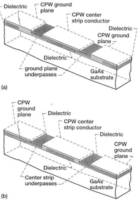
Micromachined CPWFIGURE 1.2 Schematic of a conductor-backed coplanar waveguide(CBCPW).
FIGURE 1.3 Cross section of a microshield line.(From Reference [16],IEEE 1995.) These lines are illustrated in Figures 1.3 and 1.4, respectively. The advantages of the microshield line are its extremely wide bandwidth, minimal dispersion and zero dielectric loss. The advantage of the later CPW is that it is compatible with commercial CMOSfoundry process and hence, is capable of monolithi-cally integrating CMOSdevices and circuits.
1.3 SOFTWARE TOOLS FOR COPLANAR WAVEGUIDE CIRCUIT SIMULATION
FIGURE 1.4 Cross section of a coplanar waveguide suspended by a silicon dioxide membrane over a micromachined substrate.(From Reference [17],IEEE 1997.)
mercially available [5], [18] to [21]. In addition electromagnetic simulation software for 2-D and 3-D structures have also become commercially available [21] to [25].
1.4 TYPICAL APPLICATIONS OF COPLANAR WAVEGUIDES
1.4.1 Amplifiers, Active Combiners, Frequency Doublers, Mixers, and Switches
The CPW amplifier circuits include millimeter-wave amplifiers [26], [27], distributed amplifiers [28], [29], cryogenically cooled amplifiers [30], cascode amplifiers [31], transimpedance amplifiers [32], dual gate HEMT amplifiers [33], and low-noise amplifiers [34]. The CPW active combiners and frequency doublers are described in [35] and [36], respectively. The CPW mixer circuits include ultra-small drop in mixers [37], beam lead diode double-balanced mixers [38], harmonic mixers [39], MMIC double-balanced mixers [40], [41] and double-balanced image rejection, MESFET mixers [42]. The CPW PIN diode SPDT switches are described in [43] and [44].
1.4.2 Microelectromechanical Systems (MEMS) Metal Membrane Capacitive Switches
the conductors are located on the top surface of a substrate which makes it ideally suited for fabricating metal membrane, capacitive, shunt-type switches [45]. CPW MEMSshunt switches with good insertion loss characteristics, reasonable switching voltages, fast switching speed, and excellent linearity have recently been demonstrated [45]. These switches offer, the potential to built new generation of low-loss high-linearity microwave circuits for phased array antennas and communication systems.
1.4.3 Thin Film High-Temperature Superconducting /Ferroelectric Tunable Circuits and Components
Recent advances made in the area of thin film deposition techniques, such as sputtering, laser ablation and chemical vapor deposition, and etching technolo-gies, have resulted in the application of high temperature superconducting (HTS) materials to microwave circuits [46]. The HTScircuits have low microwave surface resistance over a wide range of frequencies. As a result signal propagation takes place along these transmission lines with negligible amount of attenuation. Furthermore the advantage of using CPW is that only one surface of the substrate needs to be coated with HTSmaterial before patterning. Recently HTSlow-pass and band-stop CPW filters have been demonstrated in [47] and [48], respectively.
In addition by incorporating ferroelectric materials such as, SrTiO with HTSmaterials such as, YBa
CuO\V, low-loss, voltage-tunable MMICs with reduced length scales can be constructed [49] and [50]. These MMICs have potential applications in phased array antenna systems and frequency agile communications systems. Recently voltage tunable CPW YBa
CuO\V/ SrTiO
phaseshifters, mixers and filters have been demonstrated [50].
1.4.4 Photonic Bandgap Structures
When an electromagnetic wave propagates along a conductor backed CPW considerable amount of energy leakage takes place. The energy that leakes, propagates along the transverse directions away from the line, and excites a parallel plate mode between the CPW top and bottom ground planes. The parasitic parallel plate mode is the leading cause for crosstalk between adjacent circuits. The cross talk can be suppressed by constructing a photonic bandgap lattice on the CPW top ground planes as demonstrated in [51].
1.4.5 Printed Antennas
conductor backed CPW with a series gap in the center strip conductor is used to couple power to a patch through an aperture in the common ground plane. This design offers the flexibility of inserting semiconductor devices in the series gap of the feed for controlling the coupling.
1.5 ORGANIZATION OF THIS BOOK
This book is organized to serve as a text for a graduate course in MICs and MMICs, as well as a reference volume for scientists and engineers in industry. Chapter 1 gives an overview of the advantages, types, and typical applications of CPW.
Chapters 2 through 5 are devoted to the basic structures such as conven-tional CPW, conductor backed CPW, CPW with finite-width ground planes, elevated CPW, and CPW suspended inside a conducting enclosure. Analytical expressions to compute, the effective dielectric constant and characteristic impedance of the lines are provided.
Chapter 6 discusses coplanar stripline (CPS) and its variants. Analytical expressions to compute, the effective dielectric constant and the characteristic impedance are provided.
Coupled CPWs have several applications in the design of microwave components such as, directional couplers and filters. In Chapter 7 the even-mode and odd-even-mode characteristics of both edge coupled as well as broadside coupled CPWs are presented.
When an electromagnetic wave propagates along a CPW it suffers attenu-ation due to conductor and dielectric losses. In Chapter 8 the attenuattenu-ation characteristics of conventional, micromachined, and superconducting CPWs are discussed.
Discontinuities such as, open circuits and circuit elements, such as air-bridges, are an integral part of practical CPW circuits. A good understanding of their characteristics is essential for design success. Hence Chapter 9 is devoted to CPW discontinuities.
Transitions between CPW and other transmission media are essential for integrating various components and subsystems into a complete system. Chapter 10 presents transitions between CPW and the following transmission lines: microstrip, slotline, coplanar stripline, balanced stripline, and rectangular waveguide.
Coupling of power from one line to another takes place when the lines are placed in close proximity to each other. In Chapter 11 the design and construction of directional couplers are presented. These couplers can be realized using either edge coupled CPW or broadside coupled CPW. In addition the construction and design of hybrid couplers and magic-Ts are also discussed.
and phase shifters, high-temperature superconducting circuits, tunable compo-nents based on ferroelectric materials, photonic bandgap structures and printed circuit antennas.
REFERENCES
[1] C. P. Wen, ‘‘Coplanar Waveguide: A Surface Strip Transmission Line Suitable for Nonreciprocal Gyromagnetic Device Applications,’’ IEEE Trans. Microwave T heory Tech., Vol. 17, No. 12, pp. 1087—1090, Dec. 1969.
[2] J. L. B. Walker, ‘‘A Survey of European Activity on Coplanar Waveguide,’’1993 IEEE MTT-S Int. Microwave Symp. Dig.,Vol. 2, pp. 693—696, Atlanta, Georgia, June 14—18, 1993.
[3] A. K. Sharma and T. Itoh (Editors), Special Issue on Modeling and Design of Coplanar Monolithic Microwave and Millimeter-Wave Integrated Circuits,IEEE Trans. Microwave T heory Tech., Vol. 41, No. 9, Sept. 1993.
[4] T. Sporkmann, ‘‘The Evolution of Coplanar MMICs over the past 30 Years,’’ Microwave Journal, Vol. 41, No. 7, pp. 96—111, July 1998.
[5]. T. Sporkmann, ‘‘The Current State of the Art in Coplanar MMICs,’’Microwave J., Vol. 41, No. 8, pp. 60—74, Aug. 1998.
[6] J. Browne, ‘‘Broadband Amps Sport Coplanar Waveguide,’’Microwaves RF, Vol. 26, No. 2, pp. 131—134, Feb. 1987.
[7] Technology Close-Up,Microwaves RF, Vol. 27, No. 4, p. 79, April 1988.
[8] J. Browne, ‘‘Coplanar Waveguide Supports Integrated Multiplier Systems,’’ Microwaves RF, Vol. 28, No. 3, pp.137—138, March 1989.
[9] J. Browne, ‘‘Coplanar Circuits Arm Limiting Amp with 100-dB Gain,’’ Micro-waves RF, Vol. 29, No. 4, pp. 213—220, April 1990.
[10] J. Browne, ‘‘Broadband Amp Drops through Noise Floor,’’Microwaves RF, Vol. 31, No. 2, pp. 141—144, Feb. 1992.
[11] J. Browne, ‘‘Coplanar MIC Amplifier Bridges 0.5 To 18.0 GHz,’’Microwaves RF, Vol. 26, No. 6, pp. 194—195, June 1987.
[12] R. E. Stegens and D. N. Alliss, ‘‘Coplanar Microwave Integrated Circuit for Integrated Subsystems,’’Microwave Sys. News Comm. Tech., Vol. 17, No. 11, pp. 84—96, Oct. 1987.
[13] E. M. Godshalk and J. Pence, ‘‘Low-Cost Wafer Probe Scales 110-GHz Summit,’’ Microwaves RF, Vol. 32, No. 3, pp. 162—167, March 1993.
[14] S. M. J. Liu and G. G. Boll, ‘‘A New Probe for W-band On-wafer Measurements,’’ 1993 IEEE MTT-S Int. Microwave Symp., Dig.,Vol. 3, pp. 1335—1338, Atlanta, Georgia, June 14—18, 1993.
[15] R. Majidi-Ahy, M. Riaziat, C. Nishimoto, M. Glenn, S. Silverman, S. Weng, Y. C. Pao, G. Zdasiuk, S. Bandy, and Z. Tan, ‘‘5—100 GHz InP CPW MMIC 7-Section Distributed Amplifier,’’1990 IEEE Microwave Millimeter-Wave Monolithic Cir-cuits Symp. Dig., pp. 31—34, Dallas, Texas, May 7—8, 1990.
[16] T. M. Weller, L. P. B. Katehi, and G. M. Rebeiz, ‘‘High Performance Microshield Line Components,’’IEEE Trans. Microwave T heory Tech., Vol. 43, No. 3, pp. 534—543, March 1995.
[17] V. Milanovic, M. Gaitan, E. D. Bowen, and M. E. Zaghloul, Micromachined Microwave Transmission Lines in CMOSTechnology,’’IEEE Trans. Microwave T heory Tech., Vol. 45, No. 5, pp. 630—635, May 1997.
[18] R. Kulke, T. Sporkmann, D. Kother, I. Wolff, and P. Pogatzki, ‘‘Coplanar Elements Support Circuit Designs to 67 GHz, Part 1,’’Microwaves RF, Vol. 33, No. 13, pp. 103—116, Dec. 1994.
[19] R. Kulke, T. Sporkmann, D. Kother, I. Wolff, and P. Pogatzki, ‘‘Modeling and Analysis Aid Coplanar Designs, Part 2,’’ Microwaves RF, Vol. 34, No. 1, pp. 89—916, Jan. 1995.
[20] R. Kulke, T. Sporkmann, D. Kother, I. Wolff, and P. Pogatzki, ‘‘Examine the Applications of Coplanar Circuits, Part 3,’’Microwaves RF, Vol. 34, No. 2, pp. 112—117, Feb. 1995.
[21] Agilent Technologies, Santa Clara, California.
[22] J. C. Rautio, ‘‘Free EM Software Analyzes Spiral Inductor on Silicon,’’ Micro-waves RF, Vol. 38, No. 9, pp. 165—172, Sept. 1999.
[23] Zeland Software, Inc., Fremont, California. [24] Ansoft Corporation, Pittsburg, Pennsylvania. [25] Jansen Microwave GmbH, Aachen, Germany.
[26] G. S. Dow, T. N. Ton, and K. Nakano, ‘‘Q-Band Coplanar Waveguide Amplifier,’’ 1989 IEEE MTT-S Int. Microwave Symp. Dig. Vol. 2, pp. 809—812, Long Beach, California, June 13—15, 1989.
[27] K. M. Strohm, J.-F. Luy, F. Schaffler, H. Jorke, H. Kibbel, C. Rheinfelder, R. Doerner, J. Gerdes, F. J. Schmuckle, and W. Heinrich, ‘‘Coplanar Ka-Band SiGe-MMIC Amplifier,’’Electron. Lett., Vol. 31, No. 16, pp. 1353—1354, Aug. 1995. [28] M. Riaziat, S. Bandy, and G. Zdasiuk, ‘‘Coplanar Waveguides for MMICs,’’
Microwave J., Vol. 30, No. 6, pp. 125—131, June 1987.
[29] R. Majidi-Ahy, M. Riaziat, C. Nishimoto, M. Glenn, S. Silverman, S. Weng, Y. C. Pao, G. Zdasiuk, S. Bandy, and Z. Tan, ‘‘94 GHz InP MMIC Five-Section Distributed Amplifier,’’Electron. Lett., Vol. 26, No. 2, pp. 91—92, Jan. 1990. [30] A. Cappello and J. Pierro, ‘‘A 22-24-GHz Cryogenically Cooled GaAs FET
Amplifier,’’IEEE Trans. Microwave Theory Tech., Vol. 32, No. 3, pp. 226—230, March 1984.
[31] R. Majidi-Ahy, C. Nishimoto, M. Riaziat, M. Glenn, S. Silverman, S.-L. Weng, Y.-C. Pao, G. Zdasiuk, S. Bandy, and Z. Tan, ‘‘100-GHz High-Gain InP MMIC Cascode Amplifier,’’IEEE J. Solid-State Circuits, Vol. 26, No. 10, pp. 1370—1378, Oct. 1991.
[32] K. W. Kobayashi, L. T. Tran, M. D. Lammert, A. K. Oki, and D. C. Streit, ‘‘Transimpedance Bandwidth Performance of an HBT Loss-Compensated Co-planar Waveguide Distributed Amplifier,’’ Electron. Lett., Vol. 32, No. 24, pp. 2287—2288, Nov. 1996.
HEMT,’’IEEE Trans. Microwave Theory Tech., Vol. 44, No. 12, pp. 2379—2383, Dec. 1996.
[34] D. Leistner, ‘‘Low Noise Amplifier at L- and Ku-Band for Space Applications in Coplanar Technology,’’ 23rd European Microwave Conf. Proc., pp. 823—827, Madrid, Spain, Sept. 6—9, 1993.
[35] R. Majidi-Ahy, C. Nishimoto, J. Russell, W. Ou, S. Bandy, G. Zdasiuk, C. Shih, Y. C. Pao, and C. Yuen, ‘‘4-40 GHz MMIC Distributed Active Combiner with 3 dB Gain,’’Electron. Lett., Vol. 28, No. 8, pp. 739—741, April 1992.
[36] M. Riaziat, E. Par, G. Zdasiuk, S. Bandy, and M. Glenn, ‘‘Monolithic Millimeter Wave CPW Circuits,’’1989 IEEE MTT-S Int. Microwave Symp. Dig., Vol. 2, pp. 525—528, Long Beach, CA, June 13—15, 1989.
[37] D. Neuf and S. Spohrer, ‘‘Ultrasmall MIC Mixer Designed for ECM Applica-tions,’’Microwave Sys. News Comm. Tech., Vol. 15, No. 11, pp. 70—80. Oct. 1985. [38] D. Cahana, ‘‘A New, Single Plane, Double-Balanced Mixer,’’ Appl. Microwave,
Vol. 1, No. 2, pp. 78—83, Aug./Sept. 1989.
[39] J. H. Lepoff, ‘‘Mix Harmonics With Dual-Beam-Lead Diodes,’’Microwaves RF, Vol. 23, No. 5, pp. 209—212, May 1984.
[40] J. Eisenberg, J. Panelli, and W. Ou, ‘‘A New Planar Double-Double Balanced MMIC Mixer Structure,’’ 1991 IEEE Microwave Millimeter-Wave Monolithic Circuits Symp. Dig., pp. 69—72, Boston, Massachusetts, June 10—11, 1991. [41] J. A. Eisenberg, J. S. Panelli, and W. Ou, ‘‘Slotline and Coplanar Waveguide Team
to Realize a Novel MMIC Double Balanced Mixer,’’Microwave J., Vol. 35, No. 9, pp. 123—131, Sept. 1992.
[42] D. Neuf and S. Spohrer, ‘‘Double Balanced, Coplanar, Image Rejection Mixer Uses Monolithic MESFET Quad,’’1991 IEEE MTT-S Int. Microwave Symp. Dig., Vol. 2, pp. 843—846, Boston, Massachusetts, June 10—14, 1991.
[43] R. W. Waugh and R. M. Waugh, ‘‘SPDT Switch Serves PCN Applications,’’ Microwaves RF, Vol. 33, No. 1, pp. 111—118, Jan. 1994.
[44] G. E. Ponchak and R. N. Simons, ‘‘Channelized Coplanar Waveguide PIN-Diode Switches,’’19th European Microwave Conf. Proc., pp. 489—494, London, England, Sept. 4—7, 1989.
[45] C. L. Goldsmith, Z. Yao, S. Eshelman and D. Denniston, ‘‘Performance of Low-Loss RF MEMSCapacitive Switches,’’IEEE Microwave Guided Wave Lett., Vol. 8, No. 8, pp. 269—271, Aug. 1998.
[46] M. Nisenoff and W. J. Meyers (Editors), Special Issue on the Microwave and Millimeter Wave Applications of High Temperature Superconductivity, IEEE Trans. Microwave T heory Tech., Vol. 44, No. 7, Part II, July 1996.
[47] W. Chew, L. J. Bajuk, T. W. Cooley, M. C. Foote, B. D. Hunt, D. L. Rascoe, and A. L. Riley, ‘‘High-T
Superconductor Coplanar Waveguide Filter,’’IEEE Elec-tron. Device Lett., Vol. 12, No. 5, pp. 197—199, May 1991.
[48] S. Wallage, J. L. Tauritz, G. H. Tan, P. Hadley, and J. E. Mooij, ‘‘High T Superconducting CPW Bandstop Filters for Radio Astronomy Front Ends,’’ IEEE Trans. Appl. Superconductivity, Vol. 7, No. 2, pp. 3489—3491, June 1997. [49] D. C. DeGroot, J. A. Beall, R. B. Marks, and D. A. Rudman, ‘‘Microwave
Properties of Voltage-Tunable YBa
CuO\V/SrTiO Coplanar Waveguide
Transmission Lines,’’ IEEE Trans. Appl. Superconductivity, Vol. 5, No. 2, pp. 2272—2275, June 1995.
[50] A. T. Findikoglu, Q. X. Jia, and D. W. Reagor, ‘‘Superconductor/Nonlinear-Dielectric Bilayers for Tunable and Adaptive Microwave Devices,’’IEEE Trans. Appl. Superconductivity, Vol. 7, No. 2, pp. 2925—2928, June 1997.
[51] F.-R. Yang, K.-P. Ma, Y. Qian, and T. Itoh, ‘‘A Uniplanar Compact Photonic-Bandgap (UC-PBG) Structure and Its Applications for Microwave Circuits,’’ IEEE Trans. Microwave Theory Tech., Vol. 47, No. 8, pp. 1509—1514, Aug. 1999. [52] J. W. Greiser, ‘‘Coplanar Stripline Antenna,’’Microwave J., Vol. 19, No. 10, pp.
47—49, Oct. 1976.
CHAPTER 2
Conventional Coplanar
Waveguide
2.1 INTRODUCTION
The coplanar waveguide(CPW)proposed by C. P. Wen in 1969 consisted of a dielectric substrate with conductors on the top surface [1]. The conductors formed a center strip separated by a narrow gap from two ground planes on either side. The dimensions of the center strip,the gap,the thickness and permittivity of the dielectric substrate determined the effective dielectric con-stant(
),characteristic impedance (Z) and the attenuation() of the line. This basic structure has become known as the conventional CPW.
In Section 2.2 closed form expressions forandZ
for CPW variants are presented. These expressions are derived using conformal mapping techniques. The conformal mapping technique assumes a quasi-static TEM mode of propagation along the line. Section 2.3 briefly explains iterative techniques to determine quasi-static and Z
. The iterative methods considered are the relaxation method and the hybrid method. Section 2.4 presents a detailed analysis of CPW using the spectral domain method. In this method the frequency dependence ignored in the conformal mapping technique is taken into consideration. This section is supported by Appendixes 2A and 2B which present the steps involved in deriving the dyadic Green’s function and the time average power flow.
Sections 2.5 and 2.6 present an empirical formula for dispersion and synthesis formulas for dispersion and characteristic impedance respectively. Section 2.7 presents the characteristics of CPW with elevated or buried center strip conductor. Using these CPW structures very high Z
can be achieved. Section 2.8 presents the characteristics of CPW with ground plane or center strip conductor underpasses. Using these CPW structures very lowZ
can be achieved. Section 2.9 presents the field components of conventional CPW.
11
Section 2.10 presents closed form expressions for and Z
for CPW on cylindrical surfaces. Finally,Section 2.11 presents the effect of metal thickness onandZ
of conventional CPW.
2.2 CONVENTIONAL COPLANAR WAVEGUIDE ON A MULTILAYER DIELECTRIC SUBSTRATE
2.2.1 Analytical Expressions Based on Quasi-static Conformal Mapping Techniques to Determine Effective Dielectric Constant and Characteristic Impedance
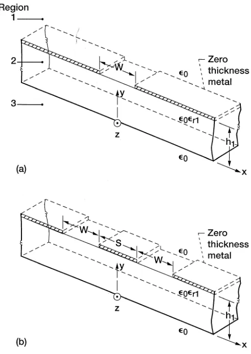
The cross-sectional view of a two coplanar waveguide (CPW) structures on multilayer dielectric substrates are shown in Figures 2.1(a)and (b). These two CPW structures are designated as sandwiched CPW and CPW on a double-layer substrate respectively. In these figures the CPW center strip conductor width S is equal to 2a and the distance of separation between the two semi-infinite ground planes in 2b. Consequently the slot width W is equal to b9a. The two dielectric substrate thicknesses are designated ash
,hand as h
, h9h in the case of sandwiched CPW and CPW on a double-layer substrate,respectively. The corresponding relative permittivities are designated as
and,respectively. Two metal covers that act as a shield are placed at a distance ofh
andhfrom the CPW conductors. The thickness of the CPW conductors ist.
In the analysis that follows,the CPW conductors and the dielectric substrates are assumed to have perfect conductivity and relative permittivity, respectively. Hence the structure is considered to be loss less. Further the dielectric substrate materials are considered to be isotropic.
In this section expressions for determining and Z
using conformal mapping techniques are presented. The assumptions made are that the conduc-tor thickness tis zero and magnetic walls are present along all the dielectric boundaries including the CPW slots. The CPW is then divided into several partial regions and the electric field is assumed to exist only in that partial region. In this manner the capacitance of each partial region is determined separately. The total capacitance is then the sum of the partial capacitances [2]. Expressions for the partial capacitances of the sandwiched CPW will be derived first and later extended to the case of CPW on a double-layer dielectric. The total capacitanceC!.5of the sandwiched CPW is the sum of the partial capacitances C, C,and C of the three partial regions shown in Figures 2.2(a) to (c). That is,
C!.5:C;C;C . (2.1)
In this equationC
FIGURE 2.1 Schematic of a CPW with top and bottom metal cover:(a)Sandwiched between two dielectric substrates;(b)on a double-layer dielectric substrate.
Calculation of C1 The capacitanceCof the lower partial dielectric region is
where the modulus of the complete elliptic integralsK(k
) andK(k) are [3]
Calculation of C2 The capacitanceCof the upper partial dielectric region is given by [3]
Calculation of Cair The capacitanceC is given by [3]
C :2
Eq.(2.1)gives
Under quasi-static approximationis defined as [3]
:C!.5
For the CPW on a double-layer dielectric substrate shown in Figure 2.1(b), the partial capacitances are determined from the structures illustrated in Figure 2.3(a) to (c). Since these structures resemble those in the previous example,Eqs.
(2.2), (2.3), (2.8),to (2.10) are still valid. However,the only change is in the equation for the partial capacitanceC
,which is as follows [3]:
Equation (2.6) for the modulus of the elliptical integral is still valid. In a manner similar to the previous case by combining the above equations an expression foris obtained which is as follows [3]:
:1;q
(91);q(9). (2.22) Equations(2.16)and(2.17)for the partial filling factorsq
andqare valid in this case also. Lastly Eq.(2.20)holds good for the characteristic impedance. In the sections that follow several limiting cases will be discussed and expressions forandZ
presented.
2.2.2 Conventional Coplanar Waveguide on an Infinitely Thick Dielectric Substrate
This structure is schematically illustrated in Figure 2.4. In order for the equations derived earlier to be applicable,we have to seth
:-,:1 and
FIGURE 2.4 Schematic of a CPW on an infinitely thick dielectric substrate.
and hence Eq.(2.8)forC simplifies to
C :4K(k) K(k
)
. (2.28)
Substituting Eqs.(2.25),(2.26),and(2.28)into Eq.(2.1)gives
C!.5:2( ;1)
K(k ) K(k
)
. (2.29)
Substituting Eqs.(2.28)and(2.29)into(2.14)gives
:1;
2 . (2.30)
Substituting Eq.(2.30)into(2.18)gives
v
:
c ((1;
)/2
, (2.31)
and Eqs.(2.19), (2.29),and(2.31)gives
Z :
30 ((
;1)/2 K(k
) K(k
)
. (2.32)
The expression forandZ
FIGURE 2.5 Schematic of a CPW on a dielectric substrate of finite thickness. 2.2.3 Conventional Coplanar Waveguide on a Dielectric Substrate of Finite Thickness
Consider the structure schematically illustrated in Figure 2.5. In this case
:1 andh
:h:-. Hence Eq.(2.2)gives
C
:2(91) K(k
)
K(k), (2.33)
wherek
andkare given by Eqs.(2.3)and(2.4),respectively. From Eqs.(2.5), when:1,we have
C
:0. (2.34)
From Eqs.(2.8)to(2.10),whenh
:h:-we have
k:k:k: S
S;2W (2.35)(a)
and
C :4K(k)
K(k). (2.35)(b)
Substituting Eqs.(2.33)to(2.35)into Eq.(2.1)gives
C
!.5:2(91) K(k
) K(k
)
;4K(k) K(k
)
which yields from Eq.(2.14),
The expression above ofandZ
is identical to those given by [4],[5]. The computedandZ
are presented in Figures 2.6(a)and(b),respectively,for a CPW on an alumina substrate.
It is worth mentioning here that in a related study [6] it has been shown that when the substrate thickness is less than twice the slot width,the deviation from the results of infinite dielectric(Section 2.2.2)is about 10 to 15 percent. Hence the propagation characteristics of lines with highZ
,and therefore large slot widths on thin substrates,should be determined using Eqs. (2.37) and
(2.38).
In [7] theZ
computed using Eq.(2.38)and by the spectral domain method are compared. The spectral domain computations are carried out at 1 GHz to avoid the effects of frequency dispersions. Table 2.1 presents this comparison. The results demonstrate that the accuracy of the conformal mapping results is better than 1 percent for a wide range of physical dimensions and available dielectric materials.
Although the conformal mapping expressions are rigorously valid at zero frequency,they can be used for the design of GaAs MMICs at millimeter wave frequencies [7]. The upper frequency limit is determined by comparing the computed quasi-static and Z
with the spectral domain values and observing the frequency at which the two sets of results deviate more than a few percent. This comparison is presented later in Section 2.6.6.
2.2.4 Conventional Coplanar Waveguide on a Finite Thickness Dielectric Substrate and with a Top Metal Cover
An upper metal shielding is inevitably present in microwave monolithic integrated circuits(MMICs) and also in hybrid circuits when flip-chip active elements are inserted [8]. This structure is schematically illustrated in Figure 2.7. In this case, :1 andh:-. Proceeding in a manner similar to the previous cases,andZ
are given by
:1;q
(91),(2.39)
FIGURE 2.6 Computed characteristics of CPW as a function ofS/(S;2W),with the normalized substrateh/bas a parameter,:10:(a)Effective dielectric constant;(b) characteristic impedance.(From Reference [4],copyrightIEE.)
where
q :
K(k
)/K(k) [K(k
)/K(k)];[K(k)/K(k)]
, (2.40)
wherek, k,andkare given by Eqs.(2.23),(2.3),and (2.10),respectively:
Z :
60 (·
1 [K(k
)/K(k)];[K(k)/K(k)]
. (2.41)
TABLE 2.1 Comparison ofZ0() of Conventional CPW with Spectral Domain Technique at 1 GHz,h1::200m,t::0
Conformal mapping Spectral Domain
a/b b(m) :20 :12.9 :2.25 :20 :12.9 :2.25
50 54.49 67.95 140.75 55.76 68.28 141.40
170 57.52 70.29 142.86 57.52 70.27 142.97
0.2 230 59.00 72.13 144.83 59.02 71.95 143.95
350 62.89 76.44 147.85 62.60 75.93 146.30
50 42.04 51.47 106.57 42.22 51.69 106.99
170 43.88 53.60 108.47 43.86 53.56 108.32
0.4 230 45.28 55.21 109.82 45.20 55.05 109.34
350 48.46 58.82 112.62 48.24 58.44 111.41
50 33.32 40.80 84.45 33.48 40.99 84.83
0.6 170 34.87 42.59 86.04 34.86 42.56 85.84
230 35.99 43.87 87.12 35.93 43.76 86.68
350 38.41 46.63 89.24 38.26 46.36 88.38
50 25.68 31.45 65.09 25.86 31.66 65.51
0.8 170 26.81 32.75 66.03 26.80 32.71 66.03
230 27.56 33.61 66.59 27.53 33.54 66.59
Source: From Reference [7],1992 IEEE.
FIGURE 2.7 Schematic of a CPW on a dielectric substrate of finite thickness and with a top metal cover.
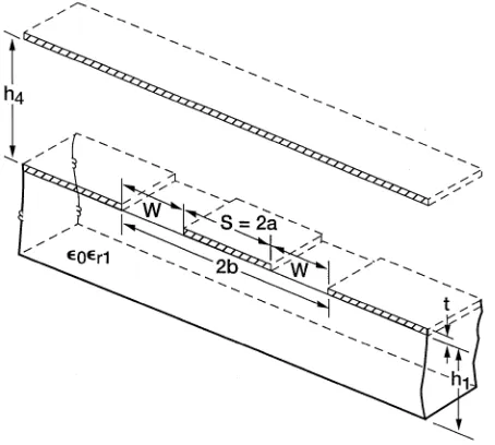
FIGURE 2.8 Schematic of a CPW sandwiched between two dielectric substrates. 2.2.5 Conventional Coplanar Waveguide Sandwiched between Two Dielectric Substrates
This structure is schematically illustrated in Figure 2.8. In this case h Substituting forK(k
) andK(k) into Eqs.(2.16)and(2.17)results in
:1;q
2.2.6 Conventional Coplanar Waveguide on a Double-Layer Dielectric Substrate
There are three variants to this structure and the first variant is shown in Figure 2.9(a). This variant follows from Figure 2.1 by lettingh
and hequal to infinity. Under these boundary conditions,Eqs. (2.42) to (2.44) derived earlier are also valid here. An expression foris obtained by substituting Eqs.
(2.43)and(2.44)into Eq.(2.22),and this is as follows: the thickness of the lower substrate,(h
9h)equal to 500m. The computed results are shown to be in good agreement with those obtained using a full wave analysis.
The second variant is shown in Fig. 2.9(b). This structure has an infinitely thick lower dielectric substrate; that is, h
is equal to infinity. Whenh:-, the capacitanceC
is given by Eq.(2.25). Equation(2.21)for the capacitance C
is also valid here. Further for hand hequal to infinity,the capacitance C is given by Eq.(2.28). KnowingC
In [7] theZcomputed using Eq.(2.50)and by the spectral domain method are compared for a wide range of parameters. The spectral domain computa-tions are carried out at 1 GHz to avoid the effect of frequency dispersion. Table 2.2 presents this comparison. The comparison shows that the accuracy of the conformal mapping results in better than 1 percent for wide range of physical dimensions and available dielectric materials.
TABLE 2.2 Comparison ofZ0() of CPW on a Double-Layer Dielectric Substrate
20 45.51 55.96 55.91 45.85 56.37 56.33
60 33.24 40.90 40.79 33.38 41.08 40.98
20 120 27.68 34.11 33.90 27.12 34.16 33.96
200 24.52 30.30 29.98 24.50 30.28 29.92
800 19.01 23.73 22.60 18.83 23.72 22.47
20 61.82 76.09 75.84 62.01 76.32 76.09
60 45.81 56.46 56.07 45.83 56.50 56.14
60 120 37.73 46.62 46.01 37.67 46.56 46.00
200 32.95 40.88 39.96 32.81 40.72 39.89
800 24.41 30.99 28.69 24.05 30.56 28.43
20 70.56 86.97 86.36 70.60 87.03 86.48
60 53.26 65.80 64.98 53.18 65.71 64.97
100 120 44.09 54.65 53.92 43.90 54.44 53.42
200 38.47 47.91 46.39 38.19 47.60 46.22
800 27.98 35.76 32.61 27.48 35.16 32.25
20 83.77 103.81 101.75 83.24 103.18 101.48
60 65.28 81.22 78.85 64.80 80.66 78.94
200 120 54.87 68.62 65.81 54.31 67.95 65.44
200 48.95 60.58 57.26 47.50 59.80 56.22
800 34.42 44.60 39.47 33.66 43.65 38.95
Source: From Reference [7],1992 IEEE.
To demonstrate that the quasi-static TEM mode has very small dispersion, the and Z
are computed using the spectral domain technique [10] and presented in Table 2.3 [7]. Table 2.3 shows that in the case of a CPW with slot width and strip width of 200 and 120m,respectively,on a 200m thick GaAs substrate(:12.9) backed by a thick quartz substrate(:3.78),the devi-ation in
andZat 45 GHz from its value at 1 GHz is as small as 2.08 and 2.19 percent,respectively. This frequency limit extends to 65 GHz with deviation in
andZof 2.23 and90.29 percent,respectively,when the slot width is reduced from 200 to 20m.
To study the effect of the lower substrate on the CPW propagation characteristics,theZ
is computed as a function of the strip width. Figure 2.10 presents the computed characteristics [7]. In this figure the slot width is held constant,and the relative permittivity of the lower substrate is used as a parameter. It is observed that the Z
TABLE 2.3 Dispersion inZ0andeffof CPW on a Double-Layer Dielectric Substrate Calculated Using Spectral Domain Technique forr1::3.78,h1::--,r2::12.9, h2::200m,t::0
W:200m andS:120m W:20mandS:120m
Z
Z
f(GHz) Z( ) (percent)
(percent) Z( ) (percent) (percent)
1 67.97 — 6.2932 — 34.16 — 6.8431 —
5 68.09 0.18 6.3014 0.05 34.17 0.03 6.8448 0.02
10 68.32 0.51 3.3210 0.17 34.19 0.09 6.8490 0.09
15 68.57 0.88 6.3481 0.35 34.20 0.12 6.8552 0.18
20 68.81 1.24 6.3816 0.56 34.22 0.18 6.8630 0.29
25 69.03 1.56 6.4208 0.80 34.23 0.20 6.8724 0.43
30 69.22 1.84 6.4651 1.08 34.24 0.23 6.8833 0.59
35 69.36 2.05 6.5141 1.39 34.24 0.23 6.8955 0.77
40 69.44 2.16 6.5675 1.73 34.23 0.20 6.9091 0.96
45 69.46 2.19 6.6248 2.08 34.22 0.18 6.9239 1.18
50 — — — — 32.20 0.12 6.9400 1.42
55 — — — — 34.16 0.00 6.9573 1.67
60 — — — — 34.12 90.12 6.9758 1.94
65 — — — — 34.06 90.29 6.9955 2.23
Source: From Reference [7],1992 IEEE.
FIGURE 2.10 Characteristic impedance as a function of the strip width with the slot width and the relative permittivity of the infinitely thick support substrate as par-ameters,h:-,
S/h
andW /h. However, Zis more sensitive for large values ofS/hand or W /h
.
The third variant is shown in Fig. 2.9(c). In this case the structure has a top metal cover. The capacitancesC
andCare given by Eqs.(2.25)and (2.21), respectively. The capacitanceC is given by
C :2
K(k)The partial filling factorsq
andqare
The height of the shield above a certain height has negligible effect on the propagation characteristics and hence its presence can be ignored. This height is called the critical height h
. A reasonable theoretical definition for a theoretical critical shield height to ground plane separationh
/bis the height h
above which the absolute difference between the Zof the CPW in Figs. 2.9(b) and (c) is less than 0.1 percent. Figure 2.11 shows the ratioh
/b as a function of the strip width with the slot width as a parameter. As a concluding remark it is worth mentioning that in [11] the conformal mapping technique has been extended to a CPW on a three-layer dielectric substrate.
2.2.7 Experimental Validation
Effective Dielectric Constant Equation(2.37)forof a conventional CPW on a finite thickness substrate(Fig. 2.5)has been validated in [2] by comparing with the time domain reflectometer(TDR)measurements [12] made on CPW fabricated on 0.65 mm thick alumina substrate (:9.8). This comparison made at 4 GHz shows that whenW /h
FIGURE 2.11 Critical shield height to ground plane separation ratio h /b as a function of the strip width with the slot width as a parameter,
:3.78, h:-, :12.9,h:200m,andt:0.(From Reference [7],IEEE 1992.)
the error is on the order of 0.4 percent and that whenW /his approximately 3.6(thin substrate),the error is on the order of 4.5 percent [2].
Characteristic Impedance In order to validate Eq. (2.38),the computedZ is compared in Figure 2.12 with the experimental values obtained from [13], [14] and [15]. TheZ
is experimentally determined using a TDR [13],[15] or from scattering parameters(S-parameters)[14] measurements. It should be pointed out that Eq.(2.38)assumes that the ground planes extend to infinity and the conductor thickness is zero,but the CPW circuits in [13],[14] and [15] have finite size ground planes in the range of 0.05 in. to 0.138 in. and the conductor thickness is in the range of 1.8 to 15m. Further,as discussed earlier,the accuracy of the computed results depends on the ratiosW /h
and S/(S;2W). For a CPW on a thick substrate with narrow slots,W/h
is less than or equal to 0.5 andS/(S;2W)is greater or equal to 0.5. The difference between the measured and the computedZis small and is less than or equal to 3.3 percent. For a CPW on a thick substrate with fairly wide slots,W /his less than or equal to 0.5 and S/(S;2W) is in the range of 0.4 to 0.5. The difference in Z
increases to about 5.8 percent. Last,for a CPW on a thin substrate with very wide slots,W /h
is in the range of 0.5 to 2.0 andS(S;2W) is less than or equal to 0.4; the difference inZ
FIGURE 2.12 Computed and measuredZ
of CPW as a function ofS/(S;2W):(a) :9.2, h:0.05 in., S:0.05 in.; (b) :9.7, h:0.64 mm, S;2W:1.0 mm; (c)
:9.6,h:0.025 in.,S:0.02 in.
FIGURE 2.12 Continued.
2.3 QUASI-STATIC TEM ITERATIVE TECHNIQUES TO DETERMINEeff
ANDZ0
Section 2.2 discussed the application of conformal mapping method to CPW and its variants. The conformal mapping method resulted in closed form equations to calculate and Z
. The purpose of this section is to acquaint the reader with other quasi-static TEM methods,such as the relaxation method [16] and the hybrid method [17]. These methods are iterative in nature and hence is different from the conformal mapping method. They can also take into consideration nonuniform geometry and or irregular boundaries.
2.3.1 Relaxation Method
In this method the two-dimensional Laplace equation is solved along the cross section of the CPW to obtain
and Z. This is done by expanding the Laplace equation to form a simultaneous difference equation. In the numerical model the CPW is assumed to be housed inside a metal enclosure that is held at zero potential. Further the CPW conductor thickness,which is much smaller than the substrate thickness,is assumed to be zero. The numerical model is validated by comparing the computed Z
Z
. The maximum difference between the measured and modeledZvalues is 3 percent [16].
2.3.2 Hybrid Method
The hybrid method combines the Galerkin finite-element method and the conformal-mapping technique. In this method,first,Wen’s [1] mapping function is adopted,which transforms the original infinite domain into a finite image domain. This mapping also overcomes the field singularity difficulty around the strip edges. The problem is then solved in this image domain by the Galerkin finite-element method.
The computed
for conventional CPW agrees well with the conformal mapping results only for largea/bratios [17]. The computedZis almost the same as that provided by the conformal mapping method [17]. An interesting feature of this method is that it can provide the magnitude of the field components in the cross-section of the structure.
2.4 FREQUENCY-DEPENDENT TECHNIQUES FOR DISPERSION AND CHARACTERISTIC IMPEDANCE
2.4.1 Spectral Domain Method
In this section the spectral domain analysis [18,19] is presented initially for a single slot line and later extended to the case of a coupled slot line. The schematic of a single slot line on a dielectric substrate is shown in Figure 2.13(a). This structure has three regions that are defined as follows:
Region 1 forh y Region 2 for 0yh
Region 3 fory0
The structure supports a hybrid mode which can be considered as a superposi-tion of TE and TM modes.
In a planar waveguide,the fields associated with the TM and TE modes may be derived from the scalar electric potential function(x,y)and from the scalar magnetic potential function(x,y) respectively. These functions are related to the electric vector potential function (x,y) and to the magnetic vector potential function(x,y)as follows:
(x, y):(x, y)eAXk, (2.56a) (x, y):(x, y)eAXk, (2.56b)
FIGURE 2.13 Schematic of(a)slot line;(b)coupled slot line.
constant along the longitudinalz-direction. In the loss less caseis equal to
:j. (2.56c)
The scalar potential functions are solutions to the scalar Helmholtz equations in the three spatial regions and are as follows:
[
VW;(GG;)]G(x, y):0, (2.57a) [
VW;(GG;)]G(x, y):0, (2.57b) where
permeability of the three spatial regions,respectively,andi:1,2,3 defines the three spatial regions. Further let
GG; :kG 9 :kAG, i:1,2,3. (2.57c) Using Maxwell’s equations,it is possible to show that in a source-free medium, the fields associated with the TM mode can be derived from an electric vector potential function(x,y)as follows:
E
:;;(x,y)
H:j;(x,y)
. (2.58a) On substituting Eq.(2.56a),we haveERG:
Similarly the fields associated with the TE modes can be derived from a magnetic vector potential function(x,y)as follows:
E: 9j;(x,y)
H:;;(x,y)
. (2.59a) On substitution of Eq.(2.56b),we have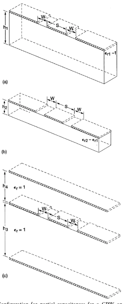


![FIGURE 2.16Measured and computed effective dielectric constant as a function of theReference [24], with permission from Microwave Exhibitions and Publishers.Ceramic:frequency: GaAs: �� � 12.9, S � 0.075 mm, W � 0.05 mm, h� � 0.4 mm, t � 0.002mm; �� � 9.8,](https://thumb-ap.123doks.com/thumbv2/123dok/4033803.1977223/66.442.107.339.309.576/effective-dielectric-thereference-permission-microwave-exhibitions-publishers-frequency.webp)