Physical Characteristics of ZnO nanorods synthesized by low
power DC thermal plasma
Ubaidillah
*,1), Suyitno
1), Wibawa Endra Juwana
1), Bayu Prabandono
1)and Agus Purwanto
2)1)
Mechanical Engineering Department, 2)Chemical Engineering Department Faculty of Engineering. Universitas Sebelas Maret (UNS)
Jl. Ir. Sutami 36 A Kentingan Surakarta 57126. Indonesia Corresponding email :*)[email protected].
Abstract:
Study on synthesis and characterization of ZnO nanorods are reported. Low power DC thermal plasma was successfully employed to fabricate these ZnO nanorods. Several testing were conducted including X-ray fluorescence (XRF), particle size analyzer (PSA), scanning electron microscopy (SEM), X-ray diffraction (XRD) and transmission electron microscopy (TEM). The diameter of resulted ZnO nanorods varies from 43 nm to 200 nm which can be seen from SEM images and its length varies from 160 nm to 1000 nm. These nanopowders are in rod shape as can be seen clearly from TEM images. The XRD data shows a sharp peak at 36.21o which indicates a good crystal growth and agrees well with the standard data (JCPDS card no. 36-1451). Effects of electrical current variations of 20, 25 and 30 Ampereere to the size of ZnO nanorods are also indicated from aspect ratio of about 8.27, 8.44 and 8.81 respectively. The ultraviolet (UV) absorption test results show that the ZnO nanorods can absorb UV with the absorbance ranges are about 300 nm and 340 nm wave lengths as well as the peak is at the wave length of 311 nm. Photoluminescence test confirm that the ZnO spectra are in blue emission with the optimum excitation wavelength of 240 nm. It can be concluded that this method is well proven in synthesizing ZnO nanorods having perfect single crystalline size, high purity compound, UV-block ability and good luminescence characteristics by spending low electrical power.
Keywords: ZnO, dc thermal plasma, nanopowders, nanorods 1. Introduction
Due to their diverse application in optical, electrical, optoelectronic, photo catalytic, hydrophilic, hydrophobic, pigments, metal compounds, medical ointments and cosmetics, nanometric ZnO such as nanospheres, nanoplates, nanosheets, nanoboxes, nanomallets, nanotripods, nanobelts, nanosprings, nanorings, nanocages, nanoneedles, nanorods, nanotubes, nanopropellers, nanoflowers and nanowindmills have been the attractive research topics in nano science and technology for few decades [1-17]. The numbers of publications significantly address this material because of its remarkable physical and chemical properties which are distinct from those of conventional bulk materials. Zinc oxide as semiconductor material has a direct band gap energy of about 3.37eV, an excitation binding energy of 60eV and tunable electrical conductivity depends on its content of charge carriers. In other benefits, this material has attracted much attention due to the ability to photo-decompose harmful bacteria [18], protect skin and eye from UV radiation without causing irritation [10]. There is also no evidence of carcinogenicity, genotoxicity and reproduction toxicity in humans [19,20].
In this study, preparation of ZnO nanorods has been performed by low power DC thermal plasma technology in which during process, the electrical power required was less than 20 kW. Variations of current inputed to the reactor were provided about 20, 25 and 30 Ampere with the rating voltage of 220 V. These are the basic difference between the previous works in [18,21,40] in which the DC thermal plasma process [18,21] employed N2 gas flow as raw
materials carrier during intake step. While in [40], after burning process, the materials are subjected to the cooling gas flown into the reactor. These two conditions make our process more superior in which it is simple and giving results of ZnO nanorods having controllable aspect ratio (L/D). Moreover, the nanoparticles shape resulted from [18,21,40] were in the form of tetrapod-like, tetrapod and rod-like , respectively. These convince us that the method used in this study is novel techniques in ZnO nanorods fabrication.
2. Experimental Setup
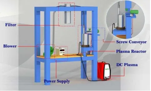
ZnO nanorods were successfully synthesized by a low power DC thermal plasma reactor as shown in Fig. 1 which was operated at atmospheric pressure and less than 20KW input plasma power. It can be seen that the reactor composed of five main parts among others screw conveyor as zinc feeder, plasma reactor as main reaction place, DC plasma as plasma power source, filter and suction blower. Commercial zinc powders (MERCK, Germany) having average particle size of about 45µm was employed in this study. The impurity of raw material has been checked using x-ray fluorescence (XRF– PANalytical-Minipal QC) and giving results of 98.98% purity of zinc and containing impurities such as P, Ca, Cr, Fe, Ni, Er and Yb.
The screw conveyor fed zinc powder into plasma reactor at the fix rate of 1.5 g/min without gas carrier. Having entered plasma reactor and faced plasma zone, vaporization and oxidation were experienced by the zinc powders immediately forming ZnO nanoparticles. The time elapsed to form ZnO nanoparticles under this process take about 0.01 s [18]. The resulted vapors from burning process were then sucked by blower passed through the filter tank so that ZnO powders could be seized by filter membrane. Electrical currents inputted to the plasma poles (cathode and anode) were varied from 20, 25, 30 and 40 Ampere.
Figure 1 Experimental setup of low power DC thermal plasma reactor
Several testing were conducted to examine the resulted ZnO nanopowders such as X-ray fluorescence (XRF), particle size analysis (PSA), X-ray diffraction (XRD) and transmission electron microscopy (TEM). To ensure the purity of synthesized rod-like ZnO nanopowders, XRF (PANalytical-Minipal QC) operated at 20kV was used as qualitative and quantitative elemental analysis. The average length of nanopowders has also been investigated using particle size analyzer DELSATM NANO at operating temperature of 25oC, scattering intensity of 10250 cps and refractive index of 1.3611.
In terms of crystallite size and phase identification, examination of the as-prepared ZnO nanorods involved X-ray diffraction analysis by the 2-2θ method. XRD (PHILLIP-XPERT PRO) was equipped with Cu Kα1 (λ=0.154060
nm) radiation at 40 kV and 30 mA. For each step, the scanning step size and collection time were set at 0.02o and 0.5 s respectively. Scanning electron microscope (FEI-Inspect S50) operated at 20 kV was used to capture the morphology of the synthesized ZnO nanorods. The individual structure and microstructural analysis were observed using transmission electron microscope (JEOL, JEM-1400) operating at 120 kV.
The optical behavior of resulted ZnO nanorods has been characterized in UV absorption and photoluminescence tests. The absorbance characteristics test was conducted in UV/VIS spectrometer (LAMBDA 25 / PERKINELMER, Singapore). Photoluminescence (PL) characterization was done in luminescence spectrometer (LS 55/PERKINELMER, Singapore). The parameters used in PLE and PL test were emission and excitation slits of 5nm and scanning speed of 500nm/min.
3. Results and Discussion
low power DC thermal plasma is effective for fabricating ZnO nanorods with the results of more than 98 percents or
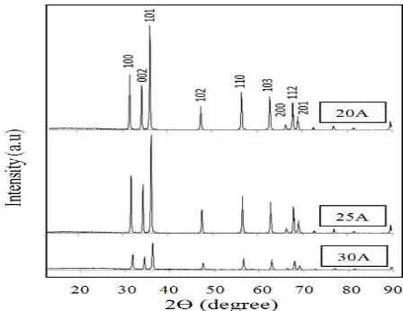
Figure 2 shows the XRD paterns of resulted ZnO nanorods. In this study, each crystalline structure of ZnO nanorods is a perfect crystal with the growth direction in c axis. Three XRD paterns is indexed as hexagonal wurtzite structure of ZnO having space group of P63mc with lattice constant sets of a,b=3.2488 Ǻ dan c=5.2049 Ǻ which is consistent with the values in the database of JCPDS 36-1451. Eight peaks appear at 2θ = 31.7o, 34.3o, 36.2o,47.5o, 56.5o, 62.8o, 66.3o, 67.9o respective to miller indexes of (100), (002), (101), (102), (110), (103) and (112). From the figure, impurities indicated by unusual ZnO diffraction peaks are not found in the XRD paterns. It confirms the high purity of the ZnO nanorods. The peaks of each miller index almost reduce in the increement of applied currents. This will affect the nano-crystalline size. The phenomena may caused by the increment of electric power supplied which makes the higher plasma temperature. It can be explained that when zinc materials are subjected to the higher temperature, the temperature difference in oxidation process will affect the cristal growth. In this case, the opportunity of the cristal to grow in lower difference temperature is better than the higher one in equal oxidation time.
Moreover, the strong and narrow intensity diffraction peaks imply the good crystalline nature and size of the synthesized products. Average nano-crystalline sizes (D) obtained from the broadening of XRD peaks are calculated using Scherer’s formula as follows [21]:
(1)
where D is the crystal size, B the broadening from the sample or its full width half medium (FWHM), λ the wave length of X-ray, θ the Bragg’s angle. Calculation results using Equation (1) are listed in Table 2.
Table 2 FWHM and crystalline size of ZnO by different plasma current
Miller index
o
2Th. FWHM Crystalline size (nm)
20A 25A 30A 20A 25A 30A
(100) 31.7401 0,1771 0,1968 0,2362 46,0038 41,4060 34,5071
(002) 34.3890 0,1378 0,1378 0,0984 60,9293 60,9415 85,3593
(101) 36.2199 0,1181 0,1771 0,1378 72,7204 48,5035 62,3431
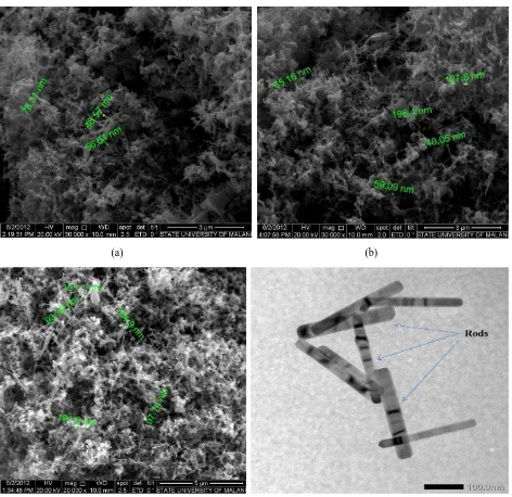
The micrographs of synthesized powders are depicted in Figure 3(a), (b) and (c) by various input currents of 20, 25 and 30 Amperes, respectively. ZnO nanorods with diameters ranging from 40 nm to 160 nm have been prepared conveniently using low power DC thermal plasma. The average length of the products and average diameter observed from SEM micrographs are tabulated in Table 3. Length to diameter ratio of ZnO nanorods has been calculated resulting in the value of 8.27, 8.44 and 8.81. Figure 3(d) depicts typical transmission electron microscopy image of ZnO nanorods for 25 Ampere current applied. It shows similar morphology as that of the SEM observations. The ZnO nanorods shown in Figure 3(d) have uniform length, straight and smooth shape.
(a) (b)
Table 3 Length to diameter ratio of ZnO nanorods Num Variable Variation (nm)
20 A 25 A 30 A 1 Average Diameter (D) 71.95 88.58 91.74 2 Average Length (L) 594.9 747.8 807.8
3 L/D 8.27 8.44 8.81
The UV absorption characteristic of the ZnO nanorods obtained from DC thermal plasma in current variation is shown in Figure 4. The ability to absorb UV increases by the increment of applied currents which is not too different in each peak. The absorbance ranges are about 300 nm and 340 nm wave lengths as well as the peak is at the wave length of 311 nm which is classified to short UV.Moreover, the as-prepared ZnO nanorods exhibit high UV-blocking capacity in which it is useful in cosmetics application such as sun block. However, it still needs more investigation of the resulted ZnO nanorods to ensure the safety issues.
Figure 4 UV absorbance characteristics
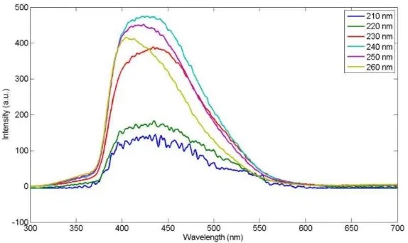
To know the optimum excitation wave length to get the highest intensity of the ZnO nanorods samples, photoluminescence excitation (PLE) is investigated in emission wavelength of 385 nm. The PLE spectra shown in Figure 5 shows that the absorbtion peaks are around 210 nm to 260 nm. From the figure, it can be seen that there is no significant difference between the particles resulted by 20 Ampere and 25 Ampere. This may due to the excited wavelength which is not the optimum for the absorbtion of photon occurred [50]. However, the optimum wavelength required for the optimum emission can be defined from the spectra. After several investigations by applying emissions of 210, 220, 230, 240, 250 and 260 nm to the samperele of 20 Ampere applied current as shown in Figure 6, the optimum excited wavelength is around 240 nm. This value will then be used as PL test parameter of all samples.
Figure 6 Peak emission test of ZnO nanorods prepared by 20 Ampere applied current
Figure 7 shows PL spectra of ZnO nanorods under several current variations at excited wavelength of about 240 nm. The peaks of luminescence intensity increase by the increment of applied currents in which all behavior belong to blue emission since the wavelength lies on between 350 nm until 550 nm. The luminescence characteristics of ZnO nanorods resulted from this plasma process can be achieved by applying relatively simple method. In comparison, blue emission of ZnO has been obtained by [51] via non equilibrium process-including laser ablation in liquid and subsequent zinc-rich annealing. Other method has also proposed by [52] in which blue emission of ZnO particles were obtained with an additional calcium doping (ZnO:Ca) via sol gel process. It can be seen that the proposed DC thermal plasma is simpler and potential to be adopted for ZnO nanorods mass product.
Figure 7 PL spectra of ZnO nanorods by DC thermal plasma
4. Conclusion
Low power DC thermal plasma was proven to be used as ZnO nanorods fabrication. It has been confirmed from XRD examination and XRF test that the resulted powders gave perfect crystalline size and high purity compound with wurtzite structure. The diameter regime was 40 nm to 160 nm and its average length is 594.9 nm to 807.0 nm, even up to 1000 nm. The consistence of length to diameter ratio has been investigated through both calculation and SEM and TEM micrographs observation. The absorbance behavior ensures ZnO ability to absorb short UV so that the resulted powder is also potential for UV protection. The luminescence characteristic also informs that the resulted ZnO is suitable for LED application. The urgency of this method is its simplicity and potential use for future large-scale preparation of nano ZnO which is useful for many important applications in human being.
5. Acknowledgement
6. References
[1] A. Moezzi, A.M. McDonagh, M.B. Cortie, Chemical Engineering Journal 185-186 (2012) 1-22. [2] T.X. Wang, T.J Lou, Mater. Lett. G2 (2008) 2329-2331.
[3] Z.L. Wang, Mater. Today 7 (2004) 26-33.
[4] J.S. Jang, C.J. Yu, S.H. Choi, S.M. Ji, E.S. Kim, J.S. Lee, J. Catal. 254 (2008) 144-155. [5] S. Mahmud, M. Johar Abdullah, M.Z. Zakaria, Proc. IMFP (2005).
[6] K. Kakiuchi, E. Hosono, T. Kimura, H. Imai, S. Fujihara, J. Sol-Gel Sci. Technol. 39 (2006) 63-72. [7] S. Mahmud, M.J. Abdullah, IEEE Conf. Emerging Technol.-Nanoelectron. (2006) 442-446. [8] L. Shen, H. Zhang, S. Guo, Mater. Chem. Phys. 114 (2009) 580-583.
[9] Y. Ding, Z.L. Wang, Micron 40 (2009) 335-342.
[10] Z.L. Wang, J. Phys. Condens. Mater. 16 (2004) R829-R858. [11] W. Yu, C. Pan, Mater. Chem. Phys. 115 (2009) 74-79.
[12] M.N.R. Ashfold, R.P. Doherty, N.G. Ndifor-Angwafor, D.J. Riley, Y. Sun, Thin Solid Films 515 (2007) 8679-8683.
[13] U. Ozgur, I.A. Ya, C. Liu, A. Teke, M.A. Reshchikov,S. Dogan , V. Avrutin, S.J. Cho, H. Morkoc, J. Appl. Phys. 98 (2005) 041301.
[14] J. Xie, P. Li, Y. Li, Y. Wang, Y. Wei, Mater. Chem. Phys. 114 (2009) 943-947. [15] M.C. Newton, P.A. Warburton, Mater. Today 10 (2007) 50-54.
[16] C. Klingshirn, Phys. Status Solidi B 244 (2007) 3027-3073.
[17] L. Yu, F. Qu, X. Wu, Applied Surface Science 257 (2011) 7432-7435.
[18] H.-F Lin, S.-C Liao, C.-T Hu, Journal of Crystal Growth 311 (2009) 1378-1384. [19] P. Patnaik, McGraw Hill. New York. 2003.
[20] Umicore, EU Classification –Directive 67/548/EEC. [citied 22/10/2010]. Avilable from: http:www.zincchemicals.umicore.com/zcProducts/fineZincPowders/EHS/classification.htm.
[21] H.-F. Lin, S.-C. Liao, S.-W. Hung, Journal of Photochemistry and Photobiology A: Chemistry 174 (2005) 82-87. [22] B. Cheng, W. Shi, J. M. Russell-Tanner, L. Zhang, E. T. Samulski, Inorg. Chem. 45 (2006) 1208-1214.
[23] H.K. Park, D.K. Kim, C.H. Kim, J. Am. Ceram. Soc. 80 (1997) 743. [24] S.I. Hirano, Ceram. Bull. 66 (1987) 1342.
[25] D. Vorkapic, T. Matsoukas, J. Am. Ceram. Soc. 81. (1998) 2815. [26] Y.X. Li, K.J. Klabunde, Chem. Mater. 4 (1992) 611.
[27] V.R. Palkar, Nanostruct. Mater. 11 (1999) 369.
[28] C.G. Granqvist, R.A. Burhman, J. Appl. Phys. 47 (1976) 2200. [29] T.T. Kodas, Adv. Mater. 6 (1989) 180.
[30] G.L. Messing, S.C. Zhang, G.V. Jayanthi, J. Am. Ceram. Soc. 76 (1993) 2707. [31] J.P. Pollinger, G.I. Messing, J. Aerosol Sci. Technol. 19 (1993) 217.
[32] R.D. Vispute, V. Talyansky, S. Choopun, R.P. Sharma, T. Venkatesan, M. He, X. Tang, J.B. Halpern, M.G. Spencer, Y.X. Li, L.G. Salanmanca Riba, A.A. Iliadis, K.A. Jones, Appl. Phys. Lett. 73 (1998) 348.
[33] M.A. Gondal, Z.H. Yamani, Q.A. Drmosh, A. Rashid, Int. J. of Nanoparticles vol.2 no. 1/2/3/4/5/6 (2009) 119-128.
[34] K. Triphati, M. Husain, N.A. Salah, S.S. Habib, S.M.A. El-Hamidy, N.Z. Zahed, Z.H. Khan, Int. J. of Nanoparticles vol. 2 no. 1/2/3/4/5/6 (2009) 148-155.
[35] S.G. Hussain, D. Liu, X. Huang, K.M. Sulieman, S.T. Rasool, Int. J. of Nanoparticles vol. 2 no. 1/2/3/4/5/6 (2009) 443-450.
[36] I.M. Joni, A. Purwanto, F. Iskandar, M. Hazata, K. Okuyama, Chemical Engineering Journal 155 (2009) 433-441. [37] Y. Hames, Z. Alpaslan, A. Kosemen, S.E. San, Y. Yerli, Solar Energy 84 (2010) 426-431.
[38] S.B. Park, Y.C. Kang, J. Aerosol Sci. 28 (Suppl.) (1997) S473-S474.
[39] C.C Chen, P. Liu, C.H. Lu, Chemical engineering Journal 144 (2008) 509-513.
[40] T.S. Ko, S. Yang, H.C. Hsu, C.P. Chu, H.F. Lin, S.C. Liao, T.C. Lu, H.C. Kuo, W.F. Hsieh, S.C. Wang, Materials Sience and Engineering B 134 (2006) 54-58.
[41] R.N. Gayen, S. Dalui, A. Rajaram, A.K. Pal, Applied Surface Science 255 (2009) 4902-4906.
[44] D.P. Singh, Sci. Adv. Mater. 2 (2010) 245-272.
[45] M.E. Fragala, Y. Aleeva, C. Satriano, J. Nanosci. Nanotechnol. 11 (2011) 8180- 8014. [46] J. Cui, J. Phys. Chem. C. 112 (2008) 10385-10388.
[47] C. Li. G. Fang, J. Li, L. Ai, B. Dong, X. Zhao, J. Phys. Chem. C 112 (2008) 990-995.
[48] J.-T. Yan, C.-H. Chen, S.-F. Yen, C.-T. Lee, IEEE Photonics Technol. Lett. 22. (2010) 146-148. [49] S. He, Y. Liu, M. Uehara, H. Maeda, Material Science and Engineering B 137 (2007) 295-298.
[50] C. Panatarani, D. G. Muharam, B. M. Wibawa, I. M. Joni, Materials Science Forum Vol 737 (2013) pp 20-27 [51] H. Zeng, G. Duan, Y. Li, S. Yang, X. Xu and W. Cai, Adv. Funct. Mater. 20 (2010) 561-572.