i
COIN ANTENNA DESIGN
NUR FAISYA BINTI KHAIRUL NURIAL SAID
This Report is Submitted in Partial Fulfillment of Requirements for the Bachelor Degree of Electronic Engineering (Telecommunication)
Faculty of Electronic and Computer Engineering Universiti Teknikal Malaysia Melaka
ii
UNIVERSTI TEKNIKAL MALAYSIA MELAKA
FAKULTI KEJURUTERAAN ELEKTRONIK DAN KEJURUTERAAN KOMPUTER
BORANG PENGESAHAN STATUS LAPORAN PROJEK SARJANA MUDA II
Tajuk Projek : HOME EQUIPMENT CONTROL USING HOME PHONE SIGNAL
Sesi Pengajian : 2009/2010
Saya NUR FAISYA BINTI KHAIRUL NURIAL SAID
mengaku membenarkan Laporan Projek Sarjana Muda ini disimpan di Perpustakaan dengan syarat-syarat kegunaan seperti berikut:
1. Laporan adalah hakmilik Universiti Teknikal Malaysia Melaka.
2. Perpustakaan dibenarkan membuat salinan untuk tujuan pengajian sahaja.
3. Perpustakaan dibenarkan membuat salinan laporan ini sebagai bahan pertukaran antara institusi pengajian tinggi.
4. Sila tandakan ( √ ) :
SULIT* (Mengandungi maklumat yang berdarjah keselamatan atau kepentingan Malaysia seperti yang termaktub di dalam AKTA RAHSIA RASMI 1972)
TERHAD* (Mengandungi maklumat terhad yang telah ditentukan oleh organisasi/badan di mana penyelidikan dijalankan)
TIDAK TERHAD
Disahkan oleh:
__________________________ ___________________________________
(TANDATANGAN PENULIS) (COP DAN TANDATANGAN PENYELIA)
Alamat Tetap:
98, JLN DESA JAYA 3, TMN DESA JAYA,
34600 KAMUNTING,
PERAK.
Tarikh: 30 April 2010 Tarikh: ………..
iii
“I hereby declare that this report is result of my own effort except for works that have been cited clearly in the references.”
Signature : ……….
iv
“I hereby declare that I have read this report and in my opinion this report is sufficient in terms of scope and quality for the Bachelor Degree of Electronic Engineering
(Telecommunication)”
Signature : ………..
v
vi
ACKNOWLEDGEMENT
First of all, I am most grateful to Almighty ALLAH s.w.t. for blessing me with good health and ideas for completing this “Projek Sarjana Muda” successfully. I would like to show my highest gratitude to my supervisor, Encik Mohamad Zoinol Abidin Bin Abd Aziz for his invaluable support, patient, assistance and especially his encouragement to this project. I truly have learnt a lot and all this would not be without his guidance.
vii
ABSTRACT
viii
ABSTRAK
ix
CONTENT
CHAPTER CONTENT PAGE
TITLE i
VERIFICATION ii
CONFESSION iii
SUPERVISOR VERIFICATION iv
DEDICATION v
ACKNOWDGEMENT vi
ABSTRACT vii
ABSTRAK vii
CONTENT ix
LIST OF FIGURE xiv
LIST OF TABLES xviii
LIST OF ABREVIATION/ SYMBOL xix
I INTRODUCTION
1.1 INTRODUCTION OF PROJECT 1
1.2 OBJECTIVES 2
1.3 PROBLEM STATEMENTS 2
1.4 SCOPE 2
x
CHAPTER CONTENT PAGE
II LITERATURE REVIEW
2.1 INTRODCUTION OF ANTENNA 4
2.2 ANTENNA PARAMETERS 5
2.2.1 Resonant Frequency 6
2.2.2 Gain 6
2.2.3 Radiation Pattern 7
2.2.4 Efficiency 7
2.2.5 Bandwidth 8
2.3 DIELECTRIC RESONATOR ANTENNA 8
2.4 CYLINDRICAL DIELECTRIC RESONATOR ANTENNA
9
2.5 MALAYSIAN RINGGIT COINS 10
2.5.1 First Series (1967) 10
2.5.2 Second Series (1989) 11
2.6 FR4 BOARD 12
2.6.1 Cost 12
2.6.2 Electrical Performance 12
2.7 WIRELESS BLOCK DIAGRAM 13
III PROJECT METHODOLOGY
xi
3.2 PARAMETRIC STUDY 14
3.3 CALCULATION 15
3.4 SOFTWARE SIMULATION 16
3.4.1 Design I 16
3.4.1.1 Microstrip Coin Resonator Design 16 3.4.1.2 Planar Coin Resonator Design 17 3.4.1.3 Microstrip Coin Resonator with Offset
Design
17
3.4.1.4 Planar Coin Resonator with Offset Design
18
3.4.2 Design II 18
3.4.2.1 Microstrip Coin with Multiresonator Design
19
3.4.2.2 Planar Coin with Multiresonator Design
20
3.4.2.3 Microstrip Coin Resonator with Locator Design
20
3.4.2.4 Planar Coin Resonator with Locator Design
21
3.4.2.5 Coin Resonator with Ground Height Design
21
3.4.3 Design III
3.4.3.1 Microstrip Coin Resonator Design 22 3.4.3.2 Microstrip Coin with Multiresonator
Design
23
3.4.3.3 Planar Coin with Multiresonator Design
24
3.5 FABRICATION 24
3.6 MEASUREMENT 25
xii
IV COIN ANTENNA DESIGN
4.1 CYLINDRICAL DIELECTRIC RESONATOR ANTENNA
26
4.2 DESIGN CALCULATION 27
4.3 DESIGN SIMULATION 29
4.4.1 Design I 29
4.4.1.1 Microstrip Coin Resonator Design 29 4.4.1.2 Planar Coin Resonator Design 31 4.4.1.3 Microstrip Coin Resonator with Offset
Design
33
4.4.1.4 Planar Coin Resonator with Offset Design
35
4.4.2 Design II 37
4.4.2.1 Microstrip Coin with Multiresonator Design
37
4.4.2.2 Planar Coin with Multiresonator Design
40
4.4.2.3 Microstrip Coin Resonator with Locator Design
41
4.4.2.4 Planar Coin Resonator with Locator Design
43
4.4.2.5 Coin Resonator with Ground Height Design
44
4.4.3 Design III 47
4.4.3.1 Microstrip Coin Resonator Design 47 4.4.3.2 Microstrip Coin with Multiresonator
Design
48
4.4.3.3 Planar Coin with Multiresonator Design
xiii
4.4 FABRICATION PROCESS 51
4.5 MEASUREMENT PROCESS 54
V RESULT DISCUSSION AND ANALYSIS
5.1 OBSERVATION 57
5.2 FACTORS THAT AFFECT THE RESULTS OF MEASUREMENT
59
VI CONCLUSION
6.1 CONCLUSION 60
6.2 FUTURE WORK 61
REFERENCES 62
xiv
LIST OF FIGURE
NO TITLE PAGE
1.1 Flow Chart of Methodology 3
2.1 Radiation Pattern of DRA in 3D 7
2.2 Cylindrical Dielectric Resonator Antenna over a Ground Plane
9
2.5 Wireless Block Diagram 13
3.4 Microstrip Coin Resonator Design before Simulate by CST Software
17
3.5 Microstrip Coin Resonator with Offset Design before Simulate by CST Software
18
3.6 Microstrip Coin Resonator with Multiresonator Design before Simulate by CST Software
19
3.7 Microstrip Coin Resonator with Locator Design before Simulate by CST Software
20
3.8 Coin Resonator with Ground Height Design of 1 mm before Simulate by CST Software
21
3.9 Coin Resonator with Ground Height Design of 28 mm before Simulate by CST Software
22
3.10 Microstrip Coin Resonator Design before Simulate by CST Software
23
3.11 Microstrip Coin Resonator with Multiresonator Design before Simulate by CST Software
xv
NO TITLE PAGE
4.1 Cylindrical Dielectric Resonator Antenna 27
4.3 Microstrip Coin Resonator Design by using Simulation 30 4.4 Result of Microstrip Coin Resonator Design by using
Simulation for Frequency versus Thickness
30
4.5 Result of Microstrip Coin Resonator Design by using Simulation for Return Loss versus Thickness
31
4.6 Planar Coin Resonator Design by using Simulation 32 4.7 Result of Planar Coin Resonator Design by using
Simulation for Frequency versus Thickness
32
4.8 Result of Planar Coin Resonator Design by using Simulation for Return Loss versus Thickness
33
4.9 Microstrip Coin Resonator with Offset Design by using Simulation
34
4.10 Result of Microstrip Coin Resonator with Offset Design by using Simulation for Frequency versus Thickness
34
4.11 Result of Microstrip Coin Resonator with Offset Design by using Simulation for Return Loss versus Thickness
35
4.12 Planar Coin Resonator with Offset Design by using Simulation
36
4.13 Result of Planar Coin Resonator with Offset Design by using Simulation for Frequency versus Thickness
36
4.14 Result of Planar Coin Resonator with Offset Design by using Simulation for Return Loss versus Thickness
37
4.15 Microstrip Coin Resonator with Multiresonator Design by using Simulation for Three Coins
38
4.16 Microstrip Coin Resonator with Multiresonator Design by using Simulation for Ten Coins
xvi
NO TITLE PAGE
4.17 Result of Microstrip Coin Resonator with Multiresonator Design by using Simulation for Frequency versus Multiresonator
39
4.18 Result of Microstrip Coin Resonator with Multiresonator Design by using Simulation for Return Loss versus Multiresonator
39
4.19 Result of Planar Coin Resonator with Multiresonator Design by using Simulation for Frequency versus Multiresonator
40
4.20 Result of Planar Coin Resonator with Multiresonator Design by using Simulation for Return Loss versus Multiresonator
41
4.21 Result of Microstrip Coin Resonator with Locator Design by using Simulation for Frequency versus Coin Locator
42
4.22 Result of Microstrip Coin Resonator with Locator Design by using Simulation for Return Loss versus Coin Locator
42
4.23 Result of Planar Coin Resonator with Locator Design by using Simulation for Frequency versus Coin Locator
43
4.24 Result of Planar Coin Resonator with Locator Design by using Simulation for Return Loss versus Coin Locator
44
4.25 Coin Resonator with Ground Height Design of 1 mm by using Simulation
45
4.26 Coin Resonator with Ground Height Design of 28 mm by using Simulation
45
4.27 Result of Coin Resonator with Ground Height Design by using Simulation for Frequency versus Ground Height
xvii
NO TITLE PAGE
4.28 Result of Coin Resonator with Ground Height Design by using Simulation for Return Loss versus Ground Height
46
4.29 Result of Microstrip Coin Resonator Design by using Simulation for Frequency versus Thickness
47
4.30 Result of Microstrip Coin Resonator Design by using Simulation for Return Loss versus Thickness
48
4.31 Result of Microstrip Coin Resonator with Multiresonator Design by using Simulation for Frequency versus Multiresonator
49
4.32 Result of Microstrip Coin Resonator with Multiresonator Design by using Simulation for Return Loss versus Multiresonator
49
4.33 Result of Planar Coin Resonator with Multiresonator Design by using Simulation for Frequency versus Multiresonator
50
4.34 Result of Planar Coin Resonator with Multiresonator Design by using Simulation for Return Loss versus Multiresonator
51
4.35 The exported of simulation design in CorelDraw Software 52
4.36 FR4 Board in the UV Exposure 53
4.37 FR4 Board in the Pail to Develop the Design 53
4.38 Measurement Result for Coin Resonator with Ground Height of 15 mm
54
4.39 Measurement Result for Coin Resonator with Ground Height of 2 mm
55
4.40 Measurement Result for Coin Resonator with Ground Height of 7 mm
xviii
LIST OF TABLE
NO TITLE PAGE
2.3 First Series of Malaysian Ringgit Coins 10
xix
LIST OF ABREVIATION/ SYMBOL
D - Diameter
t - Thickness
DRA - Dielectric Resonator Antenna FR4 - Flame Retardant Type 4 PCB - Printed Circuit Board Tx - Transmitter
Rx - Receiver
1
CHAPTER I
INTRODUCTION
This chapter contains about the introduction of the project where it involved of the objectives, problem statements and research scope.
1.1 Introduction of Project
The first series of cent coins were introduced in 1967 in denominations of 1 cent, 5 cent, 10 cent, 50 cent then followed by 1 ringgit coin. The second series of cent coins entered circulation in late-1989, sporting completely redesigned observes and reverses, but remaining the designs of edges, diameters and composition of the previous series. Nowadays, the 1 ringgit coins have been terminated by Bank Negara Malaysia [3].
2
1.2 Objectives
The objective of this project is to design coin antenna using the existing coins in the market with a low cost and a suitable frequency as stated in Industrial Science Medical (ISM). The coin antenna will be feed by using transmission line feeding system.
1.3 Problem Statement
This project is efficient to the environmental factors. This is because coins such as 1 cent and 5 cent are lack in used. To overcome this problem, those coins can be used to design the coin antenna. Besides that, the coin antenna will give a broader bandwidth. This is because usually the antenna comes with a narrow bandwidth.
1.4 Scope
3
1.5 Methodology
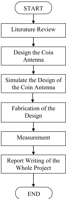
[image:22.612.274.403.190.579.2]There are few methods that have been taken to complete the project. The flow chart of the methodology is shown as Figure 1.1.
Figure 1.1: Flow Chart of Methodology END
Literature Review START
Fabrication of the Design
Measurement
Report Writing of the Whole Project Simulate the Design of
the Coin Antenna Design the Coin
4
CHAPTER II
LITERATURE REVIEW
This chapter will discuss about the theory of the antenna in terms of various types, parameter and so on. Besides that, the information of the existing coins specific in size and composition also will be explained in this chapter.
2.1 Introduction of Antenna
5
Physically, an antenna is simply an arrangement of one or more conductors, usually called elements in this context. In transmission, an alternating current is created in the elements by applying a voltage at the antenna terminals, causing the elements to radiate an electromagnetic field. In reception, for the inverse occurs, an electromagnetic field from another source induces an alternating current in the elements and a corresponding voltage at the antenna's terminals. Some receiving antennas (such as parabolic and horn types) incorporate shaped reflective surfaces to collect electromagnetic waves from free space and direct or focus them onto the actual conductive elements [1].
Antennas have practical uses for the transmission and reception of radio frequency signals such as radio and television. In air, those signals travel very quickly and with a very low transmission loss. The signals are absorbed when moving through more conductive materials, such as concrete walls or rock. When encountering an interface, the waves are partially reflected and partially transmitted through. A common antenna is a vertical rod a quarter of a wavelength long. Such antennas are simple in construction, usually inexpensive, and both radiate in and receive from all horizontal directions (omni directional). One limitation of this antenna is that it does not radiate or receive in the direction in which the rod points. This region is called the antenna blind cone or null [1].
2.2 Antenna Parameters