DESIGN OF A RF WIRELESS HEADPHONES
HAZWANI BT HATIM
This report is submitted in partial fulfillment of requirements for the award of Bachelor of Electronic Engineering (Industrial Electronics) with honours
Faculty of Electronic Engineering and Computer Engineering Universiti Teknikal Malaysia Melaka
UNIVERSITI TEKNIKAL MALAYSIA MELAKA
FAKULTI KEJURUTERAAN ELEKTRONIK DAN KEJURUTERAAN KOMPUTER
BORANG PENGESAHAN STATUS LAPORAN PROJEK SARJANA MUDA II
Tajuk Projek : ...Design of A RF Wireless Headphone...
Sesi Pengajian : .... ....2006/2007...
Saya ...HAZWANI BT HATIM...
(HURUF BESAR)
mengaku membenarkan laporan Sarjana muda ini disimpan di perpustakaan dengan syarat-syarat seperti
berikut:
1. Laporan adalah hak milik Universiti Teknikal Malaysia Melaka
2. Perpustakaan dibenarkan membuat salinan untuk tujuan pengajian sahaja
3. Perpustakaan dibenarkan membuat salinan laporan sebagai pertukaran antara institusi pengajian tinggi.
4. Sila tandakan ( √ )
(Mengandungi maklumat yang berdarjah keselamatan atau
SULIT* kepentingan Malaysia seperti yang termaktub di dalam AKTA
RAHSIA RASMI 1972)
(Mengandungi akta maklumat TERHAD yang telah ditentukan oleh
TERHAD* organisasi/badan di mana penyelidikan di jalankan.
TIDAK TERHAD
Alamat tetap: K18 D 01.04, Quarters Kediaman Kerajaan KLIA , 71800 Nilai, Negeri Sembilan
Tarikh: 27 April 2007
*CATATAN: Jika laporan ini SULIT atau TERHAD, sila lampirkan surat daripada pihak berkuasa/organisasi berkenaan dengan menyatakan sekali tempoh laporan ini perlu dikelaskan sebagai SULIT dan TERHAD.
iii
“I hereby declare that this report is the result of my own work except for quotes as cited in the references.”
Signature :
Author : Hazwani Binti Hatim
iv
“I hereby declare that I have read this report and in my opinion this report is sufficient in terms of scope and quality for the award of Bachelor of Electronic Engineering
(Industrial Electronics) with honours.”
Signature :
Supervisor’s Name : Puan Hazura Bt. Haroon
v
DEDICATION
vi
ACKNOWLEDGEMENT
Alhamdulillah, I finally able to complete the final year project and the thesis as well within the allocated time. First of all, I would like to take this opportunity to express my appreciation to some organizations and individuals who have kindly contributed to the successfully completion of my final year project in UTeM. With the cooperations and contributions from all parties, the objectives of the project; soft-skills, knowledge and experiences were gained accordingly. To begin with, I would like to convey my acknowledgement to UTeM PSM organization members especially my project supervisor, Pn Hazura Haroon for her cooperation and involvement from the begining until the end of my project development. Her effort to ensure the successfull and comfortability of students under her responsibility was simply undoubtful. Thanks for the invaluable advices given before, while and after completion of the project. Furthermore, I would like to extend my sincere acknowledgement to my parents and family members who have been very supportive throughout the project. Their understanding and support in term of moral and financial were entirely significance towards the project completion. Last but not list, my appreciation goes to my fellow colleagues in UTeM, especially for those who came from FKEKK. Their willingness to help, opinions and suggetions on some matters, advices and technical knowledge are simply precious while doing upon completion of my final year project.
vii
ABSTRACT
viii
ABSTRAK
ix
CONTENTS
CHAPTER TITLE PAGE
TITLE OF PROJECT i PENGESAHAN STATUS LAPORAN ii
DECLARATION iii
SUPERVISOR APPROVAL iv
DEDICATION v
ACKNOWLEDGEMENT vi
ABSTRACT vii
ABSTRAK viii
CONTENTS ix
LIST OF TABLE xiii LIST OF FIGURE xiv LIST OF ABBREVIATIONS xvii LIST OF APPENDIX xviii
I INTRODUCTION
1.1 OBJECTIVES 2
1.2 PROBLEM STATEMENTS 2
1.3 SCOPE OF WORK 2
1.3.1 Transmitter 3
1.3.2 Receiver 3
1.3.3 Headphone 4
x
1.4 PROJECT METHODOLOGY 4
1.4.1 Project Workflow 5 1.5 REPORT ORGANIZATION 6
II LITERATURE REVIEW
2.1 PREVIOUS STUDY AND RESEARCH 8
2.1.1 Wireless 8
2.1.2 Theory of Modulation 9 2.1.2.1 Modulation and Demodulation 10 2.1.2.2 Frequency Modulation 11 2.1.2.3 FM versus PM 12 2.1.3 Phototransistor Circuit 12
2.1.4 Filters 15
2.1.5 Phase-Locked Loops 18 2.1.5.1 PLL Loop Operation 19 2.1.6 Frequency Synthesizers 21 2.1.7 Voltage-Controlled Oscillator (VCO) 22 2.1.8 Noise Analysis 23 2.2 RECENT RELEVANT PROJECT 25 2.2.1 Behavioral Model 25 2.2.1 The Communication Model 26
III PROJECT METHODOLOGY
3.1 PROCUDERS AND METHODOLOGIES 28 3.1.1 The Process Flow Chart 29
3.2 PROJECT METHODOLOGY 30
xi 3.2.2 Design of Transceiver Circuit 30
3.2.2.1 Transmitter 30 3.2.2.2 Receiver 31 3.2.3 Simulation and Analysis Circuit 31
3.2.3.1 Proteus 6 Professional 31 3.2.4 Construct and Test Circuit 32 3.2.5 Schematic Diagram and PCB Layout 33
3.2.5.1 Overview 33 3.2.5.2 Schematic Diagram 34 3.2.5.3 PCB Layout 35 3.2.5.4 PCB Fabrication 36 3.2.5.5 Etching Process 38 3.2.5.6 Soldering Process 41 3.2.6 Testing and Demonstration 41
3.3 THE PROJECT COMPONENTS 41
3.3.1 Capacitor 42
3.3.2 Transistor 43
3.3.3 Resistor 44
3.3.4 Infrared LED 46 3.2.5 Phototransistor 48
IV RESULT AND DISCUSSION
4.1 RESULTS AND ANALYSIS OF PROJECT 49 4.1.1 Software (Simulation) 50
4.1.1.1 Transmitter Schematic 50 4.1.1.2 Receiver Schematic 52
4.1.2 Hardware 54
xii
4.1.2.3 Receiver 57
4.1.3 Comparison between Software and
Hardware 59
4.2 DISCUSSION 60
V CONCLUSION AND SUGGESTION
5.1 CONCLUSION 61
5.2 SUGGESTION 62
REFERENCES 63
xiii
LIST OF TABLE
NO TITLE PAGE
xiv
LIST OF FIGURE
NO TITLE PAGE
1.1 Block diagram of transmitter 3 1.2 Block diagram of receiver 3 1.4 GP’s Supercell primary battery 4
1.5 The Project Workflow 5
2.1 The typical waveform of the AM and FM signals 10
2.2 Common-Emitter Amplifier 13
2.3 Common-Collector Amplifier 13 2.4 Phototransistor Circuit with Base Connection 15 2.5 (a) High pass STC network 16
(b) Low pass STC network 16
2.6 Bode plot of low pass filter 16 2.7 Low Pass Filter Schematics 17 2.8 Output of the low pass filter. 17 2.9 Phase-locked loop block diagram 19 2.10 VCO versus input bias voltage characteristics 23
2.11 (a) Without noise 24
(b) Electrical Noise 24
2.12 A Behavioral Model of the Transmitter/Receiver System 26
2.13 The Communication Model 27
3.1 The process flow chart 29
xv 3.3 ISIS 6 Professional for simulation circuit 32 3.4 Circuit on the project-board 33
3.5 Window of ExpressPCB 35
3.6 PCB layout of transmitter 36
3.7 PCB layout of receiver 36
3.8 Manufacturing process chart of a single-sided PCB 37 3.9 Circuit drawing transition to transparency 38 3.10 Laminated PCB board with thin film and circuit drawing 39
3.11 UV exposure process 39
3.12 PCB board soaking process 40
3.13 Etching process 40
3.13 The soldering process 41
3.15 Type of capacitor 42
3.16 Transistor 44
3.17 (a) Variable resistors 44
(b) Permanent resistor 45
3.18 A distance between of Infra-red LED (Tx) and
Phototransistor (Rx) 46
3.19 Optoelectronic circuit symbols and a typical
emitter/detector configuration 47
3.20 Infrared Phototransistor 48
4.1 Transmitter schematic 50
4.2 (a) The output of 4 MHz 51
(b)The output of 20 MHz 51
4.3 Receiver schematic 52
4.4 The output from receiver 53 4.5 Analysis of transmitter circuit 54
4.6 The transmitter output 55
xvi
4.10 The receiver output 58
xvii
LIST OF ABREVIATIONS
RF - Radio Frequency FM - Frequency Modulation Tx - Transmitter
Rx - Receiver
Hz - Hertz
Km - Kilometers
PM - Phase Modulation
ADC - Analog-to-Digital Converter DAC - Digital-to-Analog
LED - Light Emitting Diode EM - Emitter Modulation
PIC - Peripheral Interface Controller UV - Ultra-violet
xviii
LIST OF APPENDIX
NO TITLE PAGE
A DATASHEET PNP SILICON TRANSISTO (BD 140) 64
B DATASHEET OPERATIONAL AMPLIFIER (LM741) 68
C DATASHEET LOW VOLTAGE AUDIO POWER 77 AMPLIFIER (LM 386)
D DATASHEET INRARED PHOTOTRANSISTOR 87
E DATASHEET INRARED EMITTER 91
CHAPTER I
INTRODUCTION
2
1.1 OBJECTIVES
The objectives of this project are:
i) To learn about wireless communication.
ii) To design a transmitter that is plugged into the line out and/or possible the headphone output of any audio device.
iii) To improve the size, quality and range of wireless audio communication system.
1.2 PROBLEM STATEMENTS
Using wireless communication technology for home entertainment is very popular today. Normally, headphones are connected to a wire or core from the audio device to the listening device. So people cannot enjoy listening to the radio while engaging in other activities such as yard work. This project is designed to solve this problem.
1.3 SCOPE OF WORK
3 Audio Device Audio Amplifier IR LEDs Audio Amplifier 1.3.1 Transmitter
Figure 1.1: Block diagram of transmitter
The transmitter’s block diagram is shown in Figure 1.1 which consists of an audio device, audio amplifier, and transmitter signal (IR LEDs). The transmitter is fed from an audio device, which supplies the audio signal that will be modulated and transmitted. The output signal of the audio device is already stereophonic, which means that the signal is separated into two channels, a left and a right channel. The audio signal is passed through an audio amplifier. Then, the signal will be transmitted by IR LEDs.
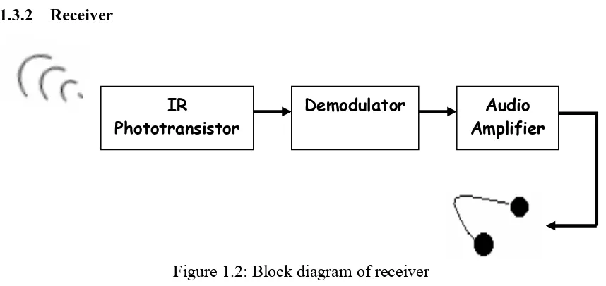
1.3.2 Receiver
Figure 1.2: Block diagram of receiver
The receiver’s block diagram that is shown in Figure 1.2 detects the transmitted signal and passes it to the headphones. The process requires the following: the signal is picked up at the transmitter’s signal. Then the demodulator comes in next to recover the information and separates the message from carrier. It produces an output voltage that is
IR
Phototransistor
[image:21.612.114.543.403.606.2]4 proportional to the instantaneous frequency of the input. The signal is passed through an audio amplifier and then the sound is heard through headphones.
1.3.4 Headphones
The output of the receiver can be connected to any headphone or speaker with 1/8 jack. In the project, two 8Ω 1W PC speakers were used.
1.3.5 Battery (GP’s Supercell)
This 9V battery is the latest in rechargeable technology and is manufactured by
[image:22.612.254.400.430.514.2]Golden Peak Group. GP's Supercell primary batteries are built to provide an economical and reliable power source for general battery operated devices. The material to make a rechargeable Ni-MH is from chemistry and this battery is mercury-free.
Figure 1.4: GP’s Supercell primary battery
1.4 PROJECT METHODOLOGY
5
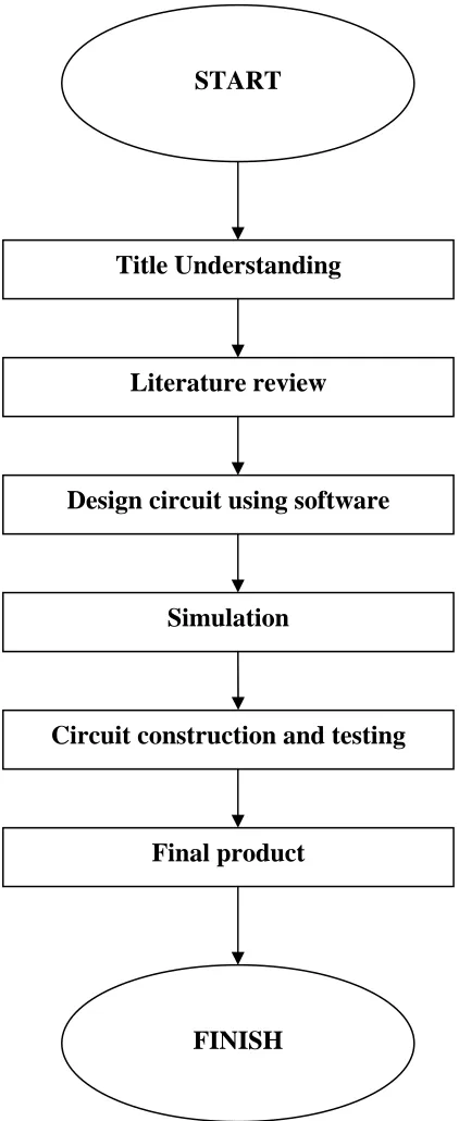
[image:23.612.220.431.119.634.2]1.4.1 Project Workflow
Figure 1.4: The project workflow START
FINISH Title Understanding
Literature review
Design circuit using software
Simulation
Circuit construction and testing
6
1.5 REPORT ORGANIZATION
This report is divided into several chapters. They are:
i. Introduction ii. Literature Review iii. Project Methodology iv. Result and Discussion v. Conclusion and Suggestion
The first chapter is an introduction to the project title. The important overview or descriptions including the objectives and scopes of the project and problem statement have been comprised.
The second chapter is the literature review about the project title. In this literature review, it includes some research about wireless, theory of modulation, basic transmission, filters, phased-looked loops and many more.
The third section is about the project methodology. In this chapter, the methods and the project flow has been explained clearly. It also includes information on the research and experiments carried out during the project development.