ARTICLES
CdTe/CdS Clusters with “Core
-
Shell” Structure in Colloids and Films: The Path of
Formation and Thermal Breakup
B. Schreder,† T. Schmidt,‡ V. Ptatschek, U. Winkler,§ A. Materny,†E. Umbach,§ M. Lerch,‡ G. Mu1ller,‡ W. Kiefer,† and L. Spanhel*,‡
Lehrstuhl fu¨r Silicatchemie der UniVersita¨t Wu¨rzburg, Ro¨ntgenring 10, 97070 Wu¨rzburg, Germany, Institut fu¨r Physikalische Chemie der UniVersita¨t Wu¨rzburg, Am Hubland, 97074 Wu¨rzburg,Germany, and Physikalisches Institut der UniVersita¨t Wu¨rzburg, Am Hubland, 97074 Wu¨rzburg, Germany
ReceiVed: May 5, 1999; In Final Form: December 23, 1999
A new organometallic “cold-slow” route to strongly fluorescing CdTe/CdS (core-shell) colloids and transparent films is presented. Based on the optical absorption, fluorescence, FTIR, micro-Raman, XPS, and XRD data collected on these nanostructures before and after thermal annealing, a mechanistic path of the core-shell formation and thermal break up is proposed and discussed. The processing of the CdTe/CdS nanostructures starts with 0.5 M tributylphosphine (TBP) stabilized CdS colloid in dichloromethane as a solvent. This yellow colloidal oil composed of 3-4 nm CdS clusters is reacted with liquid Bis(trimethylsilyl)-telluride (TMS2Te) in the presence of excess insoluble CdCl2salt. During this reaction, a rapid chalcogen
atom exchange occurs within a few seconds which produces a new CdTe “core”. The expelled sulfide reacts slowly with the CdCl2salt to form new CdS clusters after several hours. Furthermore, this
“CdS-formation-driven CdCl2salt dissolution” activates a strong green-yellow fluorescence indicating a possible evolution of
a “core-shell”-like CdTe/CdS structure. Thermal sintering of the subsequently prepared CdTe/CdS films between 100 and 200°C completely suppresses the fluorescence and initiates CdTe cluster growth, reflecting a high thermal sensitivity of the “core-shell” interfaces. By further raising the sintering temperature to 300 -400°C, the TBP ligands are released and, consequently, bare CdS- and CdTe nanocrystals, as well as ternary nanocrystalline CdTexS1-xphases, start forming. Above 400°C, the CdTe part of the nanostructures sublimates, yielding (111)-oriented CdTe films.
1. Introduction
Basic spectroscopic and structural studies on differently prepared size quantized CdTe nanoparticles have received an increased interest during the past 10 years.1-8In the meantime,
there are several synthesis routes available employing stabilizer molecules such as hexamethaphosphate,1,3 thiols,2,3,6 trioctyl
phosphine,4,7btrioctylphosphine oxide,4,7bmethanol,5,7aor
(ami-nopropyl)triethoxysilane8 to control the cluster size and the
resulting colloid stability. However, to apply the low-cost colloidal routes in designing novel optoelectronic and photo-voltaic CdTe-derived devices,9concentrated stable sols for direct
film formation are needed. To our knowledge, only the synthesis procedure described in ref 7 resulted in films of optical quality. In this paper, we address a new organometallic synthesis of CdTe/CdS (core-shell) colloids and films. The synthesis of “core-shell”-like nanostructures composed of two different semiconductors appears to be a powerful tool to control the quantum yield and the spectral response of the photolumines-cence in small nanoparticles,10 not explored so far with the
CdTe/CdS systems.
We outline the synthesis of CdTe/CdS colloids and films and discuss their structural properties based on the results collected in XRD and XPS investigations. Thereafter, we describe the optical absorption, photoluminescence, and micro-Raman prop-erties of the films as a function of the sintering temperature. Finally, we discuss the possible mechanism of buildup and thermal decomposition of the “core-shell”-like CdTe/CdS-cluster aggregates.
2. Experimental Section
Synthesis. General. All precursor solutions were prepared
in a glovebox, and the condensation reactions were carried out under Argon using the Schlenk technique. Bis(trimethylsilyl)-tellurium (TMS)2Te and Bis(trimethylsilyl)sulfur (TMS)2S
(Acros), CdCl2(99.99%), Tri-butylphosphine (TBP), heptane,
chloroform and dichloromethane (all from Aldrich) were used without further purification.
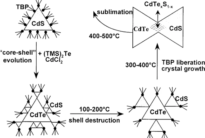
CdTe/CdS Colloids and Layers. Figure 1 shows a general flow diagram of the synthesis employed to prepare CdTe/CdS colloids and films. The detailed optimized synthesis path can be summarized as follows.
In the initial step, CdCl2 (3.66 g, 0.02 mol) powder was
suspended in 190 mL chloroform, and after 10 min of magnetic stirring at room temperature, TBP (8 g, 0.04 mol) was added
* Corresponding author: [email protected]
†Institut fu¨r Physikalische Chemie der Universita¨t Wu¨rzburg ‡Lehrstuhl fu¨r Silicatchemie der Universita¨t Wu¨rzburg. §Physikalisches Institut der Universita¨t Wu¨rzburg.
dropwise to dissolve the otherwise insoluble CdCl2powder.
After 1 h, the dissolved CdCl2 (apparently in the form of a
possible CdCl2TBP2complex) was reacted with 3.57 g (TMS)2S
(0.02 mol) to yield a yellowish stoichiometric 0.1 M CdS sol which precipitates after 30 min of stirring at 20 °C. This suspension becomes optically clear again after 15 min of refluxing. After subsequent concentration on a rotary evaporator (1 mbar, 30 °C) to remove the solvent and condensation byproducts such as (CH3)3SiCl, the resulting CdS oil was
precipitated and washed three times with heptane (removal of access TBP) and dried under vacuum (0.1 mbar, room temper-ature). The resulting powder was dissolved in dichloromethane to obtain optically transparent, intensely yellow 0.5 M CdS colloid.
In the next step, variable amounts of CdCl2powder (1.83,
3.66, or 7.32 g, i.e., 50%, 100%, or 200% excess Cd with respect to CdS) were suspended in 40 mL of the 0.5 M CdS sol followed by reaction with (TMS)2Te. It is of note that at this stage, no
additional TBP stabilizer was used! Furthermore, the molar excess-Cd-to-Te ratio was always 2. For example, if 3.66 g CdCl2(0.02 mol) were added to the TBP-capped CdS particles,
2.74 g (TMS)2Te (0.01 mol) have been subsequently added.
Immediately after the addition of the Te precursor to the CdCl2
salt-CdS particle suspension, the liquid colloidal phase became orange to red (depending upon the Te content) within a few
minutes, whereas it took about 10-30 h until the white CdCl2 salt was dissolved completely.
Finally, the optically transparent CdTe/CdS heterosols (stable for weeks) were pressed through micropore filters to remove dust particles and further used to prepare thin films via spin-on technique. For this purpose, precleaned commercial glass slides served as substrates. Typically, the substrate rotation speed and time were adjusted to 600 rpm and 10-15 s, respectively. Thereafter, the wet films were directly transferred into a sintering oven and thermally cured between 100 and 500°C for 1 h under vacuum conditions. The FTIR investigations of the films sintered at different temperatures revealed the liberation of the TBP organics at around 300°C. On layers sintered above 450°C, the characteristic CH vibrations were no longer detected in the FTIR spectra.
Optical Characterization. Optical absorption spectra of the CdTe/CdS layers were collected at room temperature with an Hitachi U 3000 UV/Vis spectrophotometer. Steady state fluo-rescence spectra were taken with a Perkin-Elmer LS50 spectrofluorimeter. For the measurements of the 0.1-0.5 M CdTe/CdS colloids, 100µm Suprasil glass cells were used. The thickness of the layers was measured with a Tencor Alpha Step 200 Profilometer.
Raman Measurements. The Raman spectra were recorded using a micro-Raman setup.11The investigated samples were
excited with the different lines of an argon ion laser (Spectra-Physics Model 166) and the 647 nm line of a krypton ion laser. The laser lines of the Ar+laser served to excite CdS nano-crystallites, whereas the krypton ion laser line was used to excite CdTe crystallites. The scattered light was analyzed by means of a double monochromator (Spex model 1404) and detected with a CCD camera (Photometrics model RDS 2000), applying the scanning multichannel technique.12The sample was placed
into a closed cycle He cryostat (CTI Cryogenics) to adjust temperatures around 10 K.
XRD Measurements. X-ray investigations on gels and films were carried out at room temperature with a STOE STADI P diffractometer (CuKR1 radiation, λ ) 1.5406 nm, Bragg -Brentano geometry). The time required to collect the XRD data was 11 h (for gels) and 2-3 h (for sintered films).
XPS InWestigations. Photoelectron spectra were recorded using tunable synchrotron radiation at the BESSY storage ring (Berlin, Germany) in combination with a SCIENTA 200 electron analyzer. Sample charging was avoided by recording the spectra with a strongly reduced photon flux. Samples suitable for XPS investigations were prepared by placing a drop of the CdS-nanoparticle solution on a cleaned Au foil and allowing the solvent to evaporate under an infrared lamp.
3. Results and Discussion
3.1. XPS- and XRD Structural Analysis of CdTe/CdS Clusters. As depicted in Figure 1 of the Experimental Section,
TBP-stabilized CdS particles act as the “seeds” in the growth of CdTe/CdS nanostructures. For the surface analysis of the washed tributylphosphine (TBP) capped CdS clusters (with sizes around 3.2(0.2 nm, see below) dispersed in dichloromethane (CH2Cl2), synchrotron X-ray photoelectron spectroscopic
meas-urements were made.
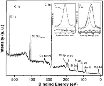
A full survey scan of the TBP-CdS nanoparticles sample is displayed in the main spectrum of Figure 2. Besides the Cd 3d core levels, the spectrum is dominated by the C 1s and O 1s signals stemming from the capping agent, remaining solvent, and sample preparation in air. The remaining components can be identified as P 2p and 2s of the stabilizing TBP molecules, Figure 1. Schematic flow diagram for the organometallic colloidal
Cl 2p representing the CH2Cl2 solvent, Si 2p and 2s of the
condensation byproduct (CH3)3SiCl, and Au 4f due to the sample
substrate.
In contrast to earlier XPS investigations on CdS clusters carrying short organic chain molecules where the Cd 3d signal exceeds by far the C 1s signal,13in the present case the C 1s
signal is much more intense than the Cd 3d one. This is mainly due to the fact that the TBP molecules in our colloid samples contain a significantly larger amount of C atoms than mercap-toethanol or propanoic acid, used as alternative stabilizer.13,14
It is evident, that the presence of such a large stabilizer shell causes a significant attenuation of the XPS signals stemming from the elements located at the cluster surface, despite the high cross section of the Cd 3d level, because photoemission is a very surface-sensitive technique. For the atoms in the interior of the clusters, the XPS-signal attenuation is even more enhanced as the signal intensity decreases exponentially with the depth of the emitting element.15 The fact that the S 2p
doublet, expected to appear at binding energy around 162 eV in a CdS environment,17is almost absent in the Figure 2 is very
interesting. It shows that the outermost shell of the TBP-CdS particles consists of Cd atoms, while the S atoms are located in their interior. Also, we cannot distinguish between inner and outer Cd atoms of the CdS particles under investigation. Fitting the Cd 3d5/2 spectrum recorded with increased experimental
resolution (Figure 2) shows the contribution of only a single component, thus, the dominance of Cd atoms at the outer surface.
The above data clearly indicate that the capping TBP molecules must be chemically bonded to Cd atoms, presumably forming tributyl-P-Cd bonds. The binding energy value of the P 2p3/2 core level (132.3 eV, see inset c in Figure 2) is in
agreement with such a chemical environment. The fact that the C atoms are more electronegative than P atoms causes a positive polarization of the latter and, thus, an increase in the binding
energy compared to P atoms in, e.g., cadmium phosphide.18The
XPS results hence show that our preparation procedure yields Cd terminated CdS particles with a TBP ligand shell bonded to them via P atoms, whereas the S atoms are located in the particle interiors. This finding is in contrast to that observed for differently prepared nanoparticles13and is consistent with the
structural models proposed recently.6,8,10,16,19 They describe
strongly quantized II-VI semiconductor clusters either as compact or as cavity-containing nonstoichiometric tetrahedrons, with cores terminated by either chalcogen or metal atoms, which depends on the synthesis conditions.
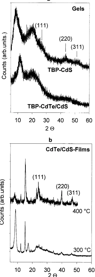
To follow the structural changes accompanying the transition from CdS to CdTe/CdS, as well as the subsequent thermal annealing of the films, XRD investigations were made. Figures 3 and 4 show the results collected on washed CdS clusters, CdTe/CdS gels (Cd:S:Te)3:1:1), and CdTe/CdS films sintered between 200 and 500°C under vacuum conditions.
The strongly broadened diffraction pattern of the starting CdS colloid (Figure 3a) showing two reflection bands at 9°and 20°, a shoulder near 26°(111), and two bumps at 44°(220) and 52° (311), indicates the presence of small “cubic” clusters. Based on the size dependent optical absorption spectra (see Figure 5, spectrum a), the CdS cluster size is estimated to be 3.2(0.2 nm, which is verified by the above XRD data. However, an attribution to a bare “zinc blende” lattice fragment is question-able since the TBP molecules must be taken into account also. The low angle diffraction peak at 9°in Figure 3a, also seen in XRD patterns of TBP precomplexed CdCl2powders prior to
the reaction with sulfide, clearly indicates that the phosphine ligands are important building blocks of the washed CdS clusters (see Experimental Section).
After the completed reaction of (TMS)2Te with CdS in the
presence of excess CdCl2 salt particles, a new peak at 12°is
quently prepared CdTe/CdS films starts at around 300°C. Table 1 summarizes the experimental findings compared to JCPDS data files of the corresponding bulk crystals.
In Figure 3b, the characteristic (111), (220), and (311) reflexes of the cubic CdTe phase can be clearly seen along with several additional reflections which we could not identify (they could stem from the crystallized organics bonded to surface terminat-ing metal atoms). By further raisterminat-ing the sinterterminat-ing temperature
to 400°C, the organic molecules start to be liberated, which allows the clusters to grow to larger CdTe nanocrystals of about 12-13 nm in size (calculated using the Debye-Warren formula). A detailed evaluation of the 300 and 400°C patterns reveals a shift of the reflexes to larger angle values with respect to a bare CdTe bulk, indicating the presence of ternary CdTe1-xSx phases (with maximum x value of ca. 0.27), also found in Raman experiments on the same films (see below). Interestingly, the binary CdS phase is not detected in film Figure 3. Experimental X-ray diffraction patterns of CdS and CdS/
CdTe gels (panel a) as well as of CdS/CdTe films thermally annealed for 1 h at 300-400°C (panel b).
Figure 4. Experimental X-ray diffraction patterns of CdTe/CdS films
samples sintered at temperatures below 400 °C. Above this temperature, where organics are increasingly liberated and no longer detected in XRD and FTIR spectra, a hexagonal CdS phase shows up in the 500°C pattern in addition to the ternary CdTe1-xSxphase (see Table 1 and Figure 4, part a). A prolonged annealing of this film sample for several hours induces CdTe vaporization. If a second glass substrate is additionally placed into the oven, CdTe condenses on it, yielding cubic zinc blende films with ca. 50 nm crystallites exhibiting a preferred (111) orientation (Figure 4, part b). To our knowledge, there exist several gas phase and solution deposition techniques, but none of them delivers (111) oriented CdTe films.
3.2. Optical Absorption and Fluorescence of CdTe/CdS Sols. Washed TBP-capped CdS nanoparticles dispersed in CH2
-Cl2 (see Experimental Section) readily react with (TMS)2Te
yielding highly concentrated orange, red, or red-brown colored sols after a few minutes. Due to the apparently lower solubility product of CdTe, a rapid exchange of the chalcogen atoms occurs, yielding sulfur enriched CdTe colloids with a weak aggregation stability and no fluorescence. However, if this process takes place in the presence of excess CdCl2salt particles,
which are insoluble in dichloromethane, two remarkable ob-servations can be made: (1) The CdCl2salt particles dissolve
completely after 10-30 h, depending upon the salt content added. Consequently, the stability of the colloid against coagulation is dramatically enhanced if the CdCl2/Te ratio is
kept g 2. Below this value, the colloids coagulate! (2) Concomitant to the CdCl2dissolution, a strong green-yellow
fluorescence is activated if at least 50% Te and 100% excess CdCl2salt are added to the starting CdS colloid.
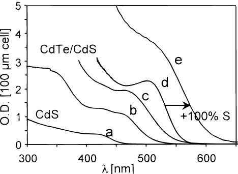
Figure 5 depicts the optical absorption spectra collected on 0.5 M CdS colloids before (spectrum a) and after (spectra b, c, and d) the completed reaction with different contents of (TMS)2Te and CdCl2salt. One recognizes an absorption onset
shifting from 460 to 570 nm with increasing Te content. Under 100% Te conditions (spectrum d), the starting CdS “cores” appear to be completely converted into new CdTe “cores” carrying a new “shell” composed of CdS, 100% remaining CdCl2, and TBP caps (see Discussion). The assumption of this
shell is supported by two facts. First, there are no excess TBP stabilizers in the above washed CdS colloids which might stabilize the CdS and CdTe separately from each other. Second,
the achieved fluorescence activation (Φfl increase from 0 to 10%) coincides with the observations made on other core-shell nanostructures,10typically prepared by combining a low band
gap with a wide band gap semiconductor.
The photoluminescence spectra of the green-yellow fluo-rescing CdTe/CdS sample produced on the addition of 100% Te and 200% Cd (with respect to Cd in the starting CdS sol) are shown in Figure 6 (spectrum a). The position of the emission maximum around 580 nm coincides with the energetic location of the optical absorption onset (see Figure 5). Unlike the (TMS)2Te, a subsequent addition of 100% (TMS)2S to the CdTe/
CdS colloid containing 100% CdCl2does not alter its
coagula-tion stability. Unexpectedly, this procedure shifts the optical absorption and photoluminescence spectra to longer wave-lengths, as indicated by the arrows in Figures 5 and 6. The corresponding sample darkening from deep red to red-brown and the change in fluorescence color from green-yellow toward red is tentatively explained in terms of an extension of the CdTe core dimension, rather than in terms of a sulfur-induced CdTe coalescence (see Discussion).
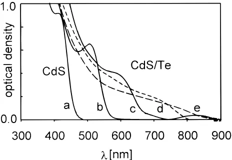
3.3. Optical Absorption and Fluorescence of Thermally Annealed CdTe/CdS Films. Figure 7 shows the effect of
increasing sintering temperature on the optical absorption spectra of heat-treated CdTe/CdS films. For comparison, the film spectrum of the CdS particles employed in the “core-shell” processing is also included. At 100°C (not shown in Figure 7), the optical absorption spectra experience a minor 5 nm red shift with respect to the wet layers before vacuum annealing (spectrum b). However, the intense green-yellow fluorescence of CdTe/CdS films completely disappears already at this relatively low temperature. This observation indicates an initial negligible tendency of the CdTe core to grow and an apparently high tendency of the surrounding CdS/CdCl2/TBP shell to
decompose, which may be responsible for the suppression of the fluorescence. Above 100°C, the film absorption onset of the strongly quantized CdTe clusters starts shifting from 600 nm to above 850 nm, reflecting the CdTe cluster growth and crystallization, also detected in our XRD investigations. Sin-tering of the films at 400°C produces 12-13 nm large CdTe nanocrystals whose optical band gap value coincides with that of the CdTe bulk (Eg)1.5 eV,λabs)826 nm, diameter of the
bulk exciton ) 9.5 nm). In Figure 7, one also recognizes a decrease in volume-normalized oscillator strength of the elec-tronic transitions with increasing CdTe dimension which coincides with the previous observations made on growing CdTe colloids.3,6Due to the substantially lower CdTe band gap, the
thermally induced optical absorption changes in the CdS part of the core-shell structures are hidden. However, during the prolonged annealing of the CdTe/CdS at 500 °C, CdTe sublimates almost completely, leaving back increasingly turbid yellow colored film samples. Their optical absorption edge is blue shifted to around 500 nm which is characteristic for CdS. On the other hand, the spectrum of the CdTe sublimate is the same as that shown for the 400°C sample in Figure 7.
An appearance of ternary phases and/or a CdS cluster growth taking place during the thermal breakup of the core-shell particles cannot be derived from the above spectral data. Therefore, highly sensitive Raman spectroscopy was chosen, which will be presented in the following section.
3.4. Resonance Micro-Raman Investigations on Thermally Annealed CdS/CdTe Films. The fluorescence in CdTe/CdS
has been shown to be a highly sensitive probe of a possible core-shell development. Unfortunately, the high fluorescence intensity of the colloids and unsintered layers did not allow us Figure 5. Optical absorption spectra of TBP-stabilized CdTe/CdS
to evaluate the cluster vibration spectra in the scope of the core -shell formation. Employing structurally inert soluble fluores-cence quenchers to remove the strong fluoresfluores-cence background was unsuccessful until now. Nevertheless, the micro-Raman studies on thermally heated CdTe/CdS films free of fluorescence enabled us to distinguish between the “cores”, the “broken shells”, and the ternary phases. The Raman spectra were taken under different excitation energy conditions to ensure the optimum resonance wavelength region for the phonon formation in size quantized and bulk-like CdS and CdTe particles.
The CdTe-core/CdS-shell system should show Raman spectra which are clearly different from those expected for a mixture of binary nanoparticles or ternary CdTe1-xSx solid solutions.
Each of the latter nanocrystalline semiconductors should show an intense 1LO phonon peak only in their respective resonance region, which is determined by the size and the size distribu-tion,20as well as by the composition.21-23For the core-shell
system we expect the CdS LO phonon peak to show resonance enhancement in the excitation region of the CdS band gap (2.5 eV) as well as in the excitation region of the CdTe band gap (1.7 eV). We also expect the presence of a kind of interface peak and the appearance of surface optical modes24,25for the
CdS-shell. Furthermore, assuming a sharp interface between the core and the shell, strains have to be taken into consideration because of the large lattice mismatch between CdTe and CdS (see Table 2). These strain effects lead to shifts of the LO phonon bands.26,27Due to the tensile strain in the CdS lattice
the CdS LO phonon peak should be red shifted, whereas the CdTe LO phonon should be blue shifted due to the compressive strain. For very small crystallites, the compression induced blue shift can be masked by a phonon confinement induced red shift and broadening of the Raman bands.28-31All of these points
will be treated in detail in the following discussion of the experimental results summarized in Figures 8 and 9.
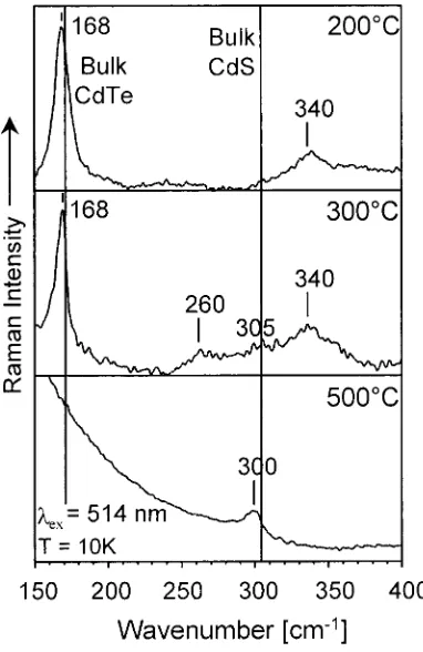
The data were taken at 10 K with CdTe/CdS films previously sintered between 200 and 500 °C. The spectra of the film samples excited at 514 (Figure 8), 458, and 647 nm (Figure 9) show distinct peaks in the region of the CdS-1LO phonon at 305 cm-1as well as in the region of the CdTe-1LO phonon
(170 cm-1) and its overtone (340 cm-1). Furthermore, a peak
at about 260 cm-1appears in the spectra of the samples heated
above 300°C.
The thermally-induced growth of the strongly quantized CdTe/CdS nanostructures causes a red shift of the energy gap (see optical spectra in Figure 7), hence also a change in the resonance conditions of CdS and CdTe. In addition, as also can be recognized in Figures 8 and 9, the intensity of the CdTe-1LO phonon peak relative to that of CdS is changing. The spectra of the 200 °C samples show an intense 1LO phonon peak of the CdTe part for all excitation wavelengths, whereas the 1LO phonon band of the CdS part was detectable only at excitation wavelengths below 465 nm. With increasing sintering temperature, the CdTe 1LO peak decreased in intensity for excitation wavelengths below 465 nm while it became very intense again at 647 nm (Figure 9c). The broad resonance region of the CdTe 1LO peak of the 200°C sample would suggest a broad size distribution of the crystallite sizes in this film, but it also could be caused by a common resonance of CdS and CdTe combined in one nanocrystallite. On the other hand, the initially weak CdS 1LO peak gained in intensity with increasing sintering TABLE 1: Theoretical and Experimental XRD Data of CdS and CdTe Bulk and Nanocrystalline Layers
2Θobs[°]
(2 2 0) 39.7 39.75 39.694 39.312 43.961
(3 1 1) 46.6 46.9 46.86 46.434 52.133
(1 0 0) 24.78 24.808
(1 0 1) 28.06 28.183
(1 1 0) 43.7 43.682
Figure 6. Photoluminescence spectra (recorded atλex)450 nm) of the TBP-stabilized CdTe/CdS colloids before and after the addition of an excess sulfide (spectrum b). The corresponding optical absorption spectra are shown in Figure 5 (spectra d and e).
Figure 7. Optical absorption spectra of CdTe/CdS films (spectra b-e) on glass before and after thermal annealing between 200°C and 400
°C in a vacuum (0.1 mbar). For comparison, the spectrum of a CdS film (spectrum a) prepared from the starting TBP/CdS colloid is also included. (b) As prepared without thermal annealing; (c) 200°C; (d) 300°C; (e) 400-500°C.
TABLE 2: Lattice Constants of CdS and CdTe Bulk Semiconductors
a (Wurtzite) a (Zinkblende)
CdS 4.137 5.838
temperature, indicating the conversion of the CdS shell into larger crystallites (Figure 9 a,b), also detected in XRD inves-tigations.
A comparison of the detected wavenumber positions of the LO phonon modes with the values of the corresponding bulk materials reveals no shift in the case of CdTe and a minor red shift in the case of CdS (Figure 9b,c). A data fit of the latter by a sum of Gaussians showed that the observed red shift is due to the appearance of a sideband at the lower energy side of the phonon band, rather than to strain effects. This sideband at a wavenumber position of about 290 cm-1is identified as the
surface optical phonon (SO) of the CdS part, which gains in significance with increasing sintering temperature and excitation wavelength. For the 400°C sample, and especially for the 500 °C sample, this peak dominates while the bulk-like CdS signal could not be resolved (Figure 9b,c).
Besides this sideband-induced shift no other shifts of the LO wavenumber position expected for highly strained CdTe/CdS nanolattices can be found (Table 1). The lack of strain deserves to be discussed in more detail. In principle, at least two possibilities exist: (1) The presence of misfit dislocations causes a reduction of the lattice quality and so a broadening of the LO phonon band as well as an appearance of the forbidden TO phonon.26,27(2) The strain does not exist because of the thermal
destruction of the core-shell nanostructures, yielding ternary phases and “bare” CdTe as well as bare CdS lattices. This second explanation is more probable than the former one since neither TO bands nor a defect broadening of the LO bands were observed. Another important indicator for this mechanism is the appearance of the phonon band at 260 cm-1. This peak can
be attributed to the CdS-like LO phonon of a ternary CdSxTe1-x
compound. Ternary CdSxTe1-xcompounds are known to exhibit
the so-called bimodal behavior.21According to this study, the
position of the CdS-like LO phonon shifts with decreasing sulfur content in the ternary phase from 306 cm-1(at x)1) to 236 cm-1(at x)0), the latter being considered as the local mode
of S in CdTe. Using their ∆ω [cm-1] vs composition-x
diagram,21 we estimate a composition around CdS 0.35Te0.65
which roughly coincides with the above-presented XRD results, indicating the presence of CdTe-dominated ternary phases, too (see section 3.1). On the other hand, the composition-dependent Raman shift of the CdTe LO phonon peak is not as pronounced. It shifts from 170 cm-1(at x)0) to 157 cm-1(at x)1), the latter being considered as the local mode of Te in CdS.21
Because of this small shift, no distinct peak of the ternary compound can be found in our data. However, the fitting of the asymmetric CdTe 1LO peak by a sum of Gaussians revealed the existence of a sideband at the low energy side of the CdTe 1LO. The wavenumber position of this sideband (at 165 cm-1)
coincides with the Raman shift value expected for the above ternary compound.
The intensity of the two peaks of the mixed compound increases whenever the CdS or the CdTe signal shows a resonance enhancement, hence, it must be due to a kind of interface layer between strongly coupled “bare” CdTe and CdS lattices. This is also supported by the fact that the Raman spectrum of the 500°C sample (Figure 9c) shows a relatively intense CdS-like 1LO phonon even at the long excitation wavelength of 647 nm. Compared with the band gap energy of large bulk-like CdS crystallites at low temperatures, this laser line is far from resonance.
3.5. Final Remarks to Development and Thermal Breakup of CdTe/CdS Nanostructures. Based on the experimental
results, we propose a possible mechanism of the formation and thermal destruction of strongly fluorescing CdTe/CdS (core -Figure 8. Raman spectra of thermally annealed CdTe/CdS films as a
function of sintering temperature. The spectra were detected at 10 K using 514 nm laser excitation. The vertical lines reflect the energetic position of the CdTe and CdS bulk lattice vibrations as indicated. The spectra show clearly the increase of the CdS LO phonon peak and a strong decrease of the CdTe LO phonon peak with increasing curing temperature.
shell) clusters in colloids and layers which is schematically depicted in Figure 10. The core-shell driven fluorescence activation starts with no fluorescing CdS clusters which are reacted with a Te-source in the presence of excess CdCl2salt
particles. Apparently, the TBP ligands do not shield completely the CdS particles, which allows chalcogen atom exchange yielding a new CdTe core and CdS shell. In previous studies performed by other groups it has been shown that on the addition of mercury to aqueous CdS colloids, the optical absorption spectra shift toward red as the result of metal atom exchange, resulting in ternary CdxHgySx+yparticles.10Our Raman study
shows that ternary CdTe1-xSxparticles seem to be accessible
only in a thermal process above 300°C, where the stabilizing ligands start liberating. In addition, the CdTe core produced in the colloidal stage is of similar size as the 3 nm large initial CdS cluster core. This could be easily proved by comparing the spectral location of the “excitonic features” in the optical absorption spectra (Figures 5 and 7) and using the energy gap/ size correlation diagrams obtained from tight binding and finite potential well calculations.6,32
We also recall the red shift in the fluorescence spectra of the prepared CdTe/CdS particles on the addition of sulfide (Figure 6), indicating a rather complex buildup of these core-shell structures. At present we can only speculate why this sulfidation step, expected to “strengthen” the shell by consuming the unreacted CdCl2, enlarges the dimension of the CdTe core by
1 nm (ca. 2 lattice constants). One possible explanation would be based on the assumption that the excess CdCl2and the TBP
ligands serve as the additional building blocks of the CdS shell, noted in XRD and XPS investigations. Such a shell would exert a large compression strain on the CdTe core. After addition of the sulfide source, the complex TBP-CdxSyClz shell would “break” causing a release of the strain and, consequently, an expansion of the CdTe core (an increase in Cd-Te bond distances). This would result in a qualitatively new, more CdS-like shell which would still passivate the surface, preserving the photoluminescence. At 100°C, as drawn in Figure 10, this highly sensitive shell breaks, resulting first in the fluorescence deactivation, second in the beginning growth of the CdTe core,
and third in the formation of larger CdS clusters seen in the Raman spectra of the 200°C film samples (Figure 9). Between 300 and 400 °C, where the TBP ligands are increasingly liberated, the core-shell structures do not exist any more; instead, aggregates composed of bare CdS and bare CdTe nanocrystals along with ternary phases start forming. Above 400 °C, the organics are completely removed and the nano-crystals are further enlarged to>10 nm. The cubic CdTe and the hexagonal CdS crystallites, strongly coupled via ternary bridges (see above discussion of the Raman data of 500°C film samples), finally decompose due to the sublimation of CdTe.
Summary
The presented study shows that an externally induced chalcogen atom exchange in CdS nanocolloids (Te against S) in the presence of undissolved CdCl2salts (without excess TBP
stabilizer) allows to synthesize stable, highly concentrated CdTe/ CdS colloidal solutions for film preparations. The achieved dramatic fluorescence activation, high coagulation stability, and significantly decreased air sensitivity compared to bare CdTe colloids can be explained assuming composite nanostructures where a CdTe core is surrounded by the CdS shell. Nevertheless, a detailed chemical analysis and HRTEM/EDX investigations will be needed to further prove the proposed core-shell structure and the above proposed mechanism (Figure 10), which goes beyond the scope of this paper. Finally, the presented XRD, optical absorption, and Raman data indicate that this new synthesis route allows to sublimate CdTe/CdS composite nanoparticles to form crystalline CdTe films with a preferred crystallographic orientation. This simple colloidal route could be an aid to all groups performing basic spectroscopic work on core-shell systems as well as solar cell research on CdS/CdTe bilayers.
Acknowledgment. We gratefully acknowledge financial
References and Notes
(1) Resch, U.; Weller, H.; Henglein, A. Langmuir 1989, 5, 1015. (2) (a) Brennan, J. G.; Siegrist, T.; Carroll, P. J.; Stuczynski, S. M.; Reynders, P.; Brus, L. E.; Steigerwald, M. L. Chem. Mater. 1990, 2, 403. (b) Stuczynski, S. M.; Brennan, J. G.; Steigerwald, M. L. Inorg. Chem.
1989, 28, 4431.
(3) Rajh, T.; Micic, O. I.; Nozik, J. J. Phys. Chem. 1993, 97, 11999. (4) Murray, C. B.; Norris, D. J.; Bawendi, M. G. J. Am. Chem. Soc.
1993, 115, 8706.
(5) Mu¨llenborn, M.; Jarvis, R. F., Jr.; Yacobi, B. G.; Kaner, R. B.; Coleman, C. C.; Haegel, N. M. Appl. Phys. A 1993, 56, 317.
(6) (a) Rogach, A. L.; Katsikas, L.; Kornowski, A.; Su, D.; Eychmu¨ller, A.; Weller, H. Ber. Bunsen-Ges. Phys. Chem. 1998, 100, 85. (b) Rocken-berger, J.; Tro¨ger, L.; Rogach, A. L.; Tischer, M.; Grundmann, M.; Eychmu¨ller, A.; Weller, H. J. Chem. Phys. 1998, 108, 7807. (c) Rocken-berger, J.; Tro¨ger, L.; Rogach, A. L.; Tischer, M.; Grundmann, M.; Weller, H.; Eychmu¨ller, A. Ber. Bunsen-Ges. Phys. Chem. 1998, 102, 85.
(7) (a) Schulz, D. L.; Pehnt, M.; Rose, D. H.; Urgiles, E.; Cahill, A. F.; Niles, D. W.; Jones, K. M.; Ellingson, R. J.; Curtis, C. J.; Ginley, D. S.
Chem. Mater. 1997, 9, 889. (b) Pehnt, M.; Schulz, D. L.; Curtis, C. J.;
Jones, K. M.; Ginley, D. S. Appl. Phys. Lett. 1995, 67, 2176.
(8) Ptatschek, V.; Schmidt, T.; Lerch, M.; Mu¨ller, G.; Emmerling, A.; Fricke, J.; Foitzik, A. H.; Spanhel, L. Ber. Bunsen-Ges. Phys. Chem. 1998,
102, 85.
(9) Aramoto, T.; Kumazawa, S.; Higichi, H.; Arita, T.; Shibutani, S.; Nishio, T.; Nakajima, J.; Tsuji, M.; Hanafusa, A.; Hibino, T.; Omura, K.; Ohyama, H.; Murozono, M. Jpn. J. Appl. Phys. 1997, 36, 6304.
(10) (a) Mews, A.; Eychmu¨ller, A. Ber. Bunsen-Ges. Phys. Chem. 1998,
102, 1343 and references therein. (b) Peng, X.; Schlamp, C.; Kadavanich,
V.; Alivisatos, A. P. J. Am. Chem. Soc. 1997, 119, 7019. (c) Tian, Y.; Newton, T.; Kotov, N. A.; Guldi, D. M.; Fendler, J. H. J. Phys. Chem.
1996, 100, 8927. (d) Danek, M.; Jensen, K. F.; Murray, Ch. B.; Bawendi,
M. G. Chem. Mater. 1996, 8, 173. (e) Kortan, A. R.; Hull, R.; Opola, R. L.; Bawendi, M. G.; Steigerwald, M. L.; Caroll, P. J.; Brus, L. E. J. Am.
Chem. Soc. 1990, 112, 1327. (f) Spanhel, L.; Haase, M.; Weller, H.;
Henglein, A. J. Am. Chem. Soc. 1987, 109, 5649.
(11) Lankers, M.; Go¨ttges, D.; Materny, A.; Schaschek, K.; Kiefer, W.
Appl. Spectrosc. 1992, 46, 1331.
(12) Deckert, V.; Kiefer, W. Appl. Spectrosc. 1992, 46, 322.
(13) (a) Winkler, U.; Eich, D.; Chen, C. H.; Fink, R.; Kulkarni, S. K.; Umbach, E. Chem. Phys. Lett. 1999, 306, 95. (b) Winkler, U., Dissertation Thesis, University of Wu¨rzburg, 1999.
(14) Resch, U.; Eychmu¨ller, A.; Haase, M.; Weller, H. Langmuir 1992,
8, 2215.
(15) Briggs, D.; Seah, M. Practical Surface Analysis; J. Wiley & Sons: Chisester, 1990; Vol. 1.
(16) Lorenz, C.; Emmerling, A.; Fricke, J.; Schmidt, T.; Hilgendorff, M.; Spanhel, L.; Mu¨ller, G. J. Non-Cryst. Solids 1998, 238, 1.
(17) Nanda, J.; Kuruvilla, B.; Sarma, D. Phys. ReV. B 1999, 59, 7473. (18) Rao, D.; Nayak, A. J. Appl. Phys. 1993, 74, 214.
(19) Behrens, S.; Bettenhausen, M.; Eichho¨fer, A.; Fenske, D. Angew.
Chem. 1997, 109, 2874 and references therein.
(20) Alivisatos, A. P.; Harris, A. L.; Levinos, N. J.; Steigerwald, M. L.; Brus, L. E. J. Chem. Phys. 1988, 89, 4001.
(21) Pal, R.; Dutta, J.; Chaudhuri, S.; Pal, A. K. J. Phys. D: Appl. Phys.
1993, 26, 704.
(22) Tu, A.; Persans, P. D. Appl. Phys. Lett. 1991, 58, 1506. (23) Olego, D. J.; Shazad, K.; Cammack, D. A.; Cornelissen, H. Phys.
ReV. B 1988, 38, 5554.
(24) Klein, M. C.; Hache, F.; Ricard, D.; Flytzanis, C. Phys. ReV. B
1990, 42, 11123.
(25) Hayashi, S.; Kanamori, H. Phys. ReV. B 1982, 26, 7079. (26) Krost, A.; Richter, W.; Zahn, D. R. T.; Brafman, O. Semicond.
Sci. Technol. 1991, 6, A109.
(27) Krost, A.; Richter, W.; Zahn, D. R. T.; Hingerl, K.; Litter, H. Appl.
Phys. Lett. 1990, 57, 1981.
(28) Shiang, J. J.; Risbud, S. H.; Alivisatos, A. P. J. Chem. Phys. 1993,
98, 8433.
(29) Tanaka, A.; Onari, S.; Arai, T. Phys. ReV. B 1992, 45, 6587. (30) Campbell, I. H.; Fauchet, P. M. Solid State Commun. 1986, 58, 739.
(31) Ptatschek, V.; Schreder, B.; Herz, K.; Hilbert, U.; Ossau, W.; Schottner, G.; Raha¨user, O.; Bischof, T.; Lermann, G.; Materny, A.; Kiefer, W.; Bacher, G.; Forchel, A.; Su, D.; Giersig, M.; Mu¨ller, G.; Spanhel, L.
J. Phys. Chem. B 1997, 101, 8898.
(32) Vossmeyer, T.; Katsikas, L.; Giersig, M.; Popovic, I. G.; Diesner, K.; Chemseddine, A.; Eychmu¨ller, A.; Weller, H. J. Phys. Chem. 1994,