A LOW-NOISE LOW-POWER SECOND-ORDER
COMPENSATED CMOS BANDGAP REFERENCE
Sigit Yuwono1, Arie van Staveren2
1Department of Electrical Engineering, Sekolah Tinggi Teknologi Telkom, Bandung–Indonesia 2Electronics Research Laboratory –Delft University of Technology, The Netherlands
1[email protected], 2[email protected]
Abstract
The design of a low-noise and low-power second-order bandgap reference voltage source using a linear combination of two base-emitter voltages with only one scaling factor is treated. The design takes into account the temperature dependency of the resistors and the finite current gain of BJT’s. The circuit is integrated in a CMOS process. The output voltage is approximately 140 mV with an average temperature dependency of 22.5 ppm/K in the range of 0°C to 120°C. Its equivalent output noise voltage is 57.6nV/√Hz. The total current consumption is about 115 μA from a 2V voltage-supply.
Keywords: bandgap reference, negative feedback, systematic design.
1. Introduction
A linear combination of two base-emitter voltages of BJT’s, whose collector biasing currents exhibit different temperature dependencies, is sufficient to perform temperature dependency compensation. If one of the scaling factors is chosen to be one then the reference voltage at the output of the bandgap reference becomes technology-determined and has first and second-order frequency temperature.
This paper describes the design of such a bandgap reference circuit with only one scaling factor and optimal noise behaviour. The design is going to be implemented on a CMOS process, therefore the reference BJT’s are of the substrate type. The design follows a systematic design approach which is concerned with optimal noise behaviour.
2. The Basic Theory and the Basic Architecture of the Bandgap Reference
Figure 1(a)[10] is a general topology of a
second-order bandgap reference. Because a1 is a constant, if a1 is shifted after the adder, Figure 1(b), the temperature dependency of the output voltage is unchanged. Thus, a1 can be removed by setting it as unity as in Figure 1(c). Figure 1(c) shows that now:
VREF = VBE1 +a2VBE2 (1)
which is a linear combination of two base-emitter voltage. Writing the base-emitter voltage as a Taylor series around a reference temperature Tr[10] results in:
) (
) (
) 0 ( ) ( ) ( ) (
2 2
'
terms order higher T
T T B
T T T V T V T V T V
r r m
r r m G r BEm r BEm BEm
(2) where:
2 1 ) ( )
( 2
2
2 m
r r m
q kT T
B (3)
q kT T
T V
V r
m r
r G m
G(0) ( ) 1 ( )
' (4)
in which α1 and α2 are the first and the second order Taylor coefficient of the bandgap voltage VG(T) at Tr, respectively, m is the number of BJT generating the base-emitter voltage, q is the electron charge, k is Boltzmann constant, θm is the order of the temperature dependency of BJTm’s biasing current
(θm =1 means a PTAT current and θm = 0 means a constant current), and η is the order of the temperature dependency of the saturation current of the BJTs. Substituting VBEm in Equation (1) with of equation (2) results in[10]:
2 ' 2 1 '
) 0 ( )
0
( G
G
REF V aV
V (4a)
) (
) (
2 2
1 2
2
B B
a (4b)
VBE1
VBE2
a1
a2
VREF
VBE1
VBE2 a2/a1
VREF
(a)
a1
(b)
VBE1
VBE2
V'REF
(c) a2
Figure 1. Second-Order Temperature Compensation:
Thus a2 is determined by the second order temperature dependency compensation. Thus VREF, which is determined by equation (4a) and (4b), is actually determined by the process selected, represented by η. For AMS CUP (a 0.60 um CMOS temperature dependency is approximately 0.6 ppm/K.
Figure 2. The Remaining 3rd-order Temperature
Dependency of VREF.
3. Technology Consideration
There are two process-dependent factors which also influences the temperature dependency of the bandgap reference circuit.
In AMS CUP process the available BJT is of PNP type so the biasing current will be more convenient expressed in the emitter current rather than in the collector current. Because the current gain, β, of the BJT available is finite, the emitter current also supplies the base current. This base current gives additional temperature dependency to the emitter voltage. The error due to the base-current is expressed as[9]:
dependency of base-current.
Another factor is the resistor used for driving the biasing current experiences also a temperature dependency. This dependency contributes additional temperature dependency to the base-emitter voltage. AMS CUP process only supplies the first order temperature dependency coefficient for its resistor, the error it contributes is[1]:
1 ( )
temperature dependency can be found. Adding these additional temperature dependencies into equation (3) and (4a) appropriately will result in a shift in value of a2, which in return also shifts the value ofVREF. The new values after taking these errors into account are: a2 = –0.88 and VREF = 134.67 mV.
4. Implementation of the Circuit
Figure 1(c) is the basic block of the bandgap reference which is going to be implemented. Its output voltage is expressed in equation (1).
VREF
Figure 3. The Bandgap Reference at Nullor Level
4.1 The Basic Circuit Diagram
Figure 3 is the bandgap reference at nullor level which implements Figure 1(c). The output of Figure 3 is expressed as:
To suit Equation (1) these conditions are required:
2
4.2 BJT Biasing
In Figure 3, BJT1 (BJT2) is biased at a PTAT
(constant) current level.
The minimum noise voltage at the output of the bandgap reference only due to the noise of the reference transistors, equals[10]:
MAX behavior following condition should be fulfilled[10]:
The saturation current of BJT1 IS1 is set equal to of the minimum sized BJT in AMS 0.6 m CUP process while the saturation current of BJT2 IS2 is set by using N times of the minimum sized BJT, in other words, IS2 = N*IS1. The relationship of all these parameters and requirements is given as[3]:
minimum current found with Equation (10). Putting IC1 and IC2 into following equation: convenient to be expressed in its emitter current. For CUP process β(Tr) = 17.29, thus:
IE1= 6.71A and IE2= 5.91A.
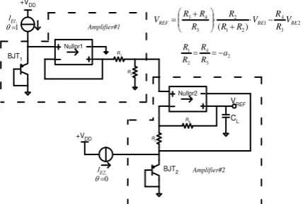
4.3 Developing the Bandgap Reference at Circuit Level
To develop the bandgap reference more systematically the basic circuit in Figure 3 is divided into two amplifiers, i.e.: Amplifier#1, includes BJT1,
Nullor1, R1 and R2, and Amplifier#2, includes BJT2,
Nullor1, R3 and R4.
The nullors consist of two stages of amplifier in order to achieve relatively high open loop gain. The input stage is a PMOS differential amplifier and the second stage is an NMOS common source amplifier in order to make the circuit operate under a single polarity voltage supply. The restriction in designing the amplifiers is that the current through the resistors must not be higher than its BJT’s emitter current.
4.3.1 Amplifier#1
Following the restriction of maximal current through the resistors R1 and R2 and fulfilling Equation (9) results in:
R1 =39.9 kΩ and R2 =45.34kΩ.
A convenient level of drain current and the dimension of PMOS for the input stage of the nullor are found by setting such a way that its noise level is a half of it produced by resistors R1 and R2. The high-frequency stability of Amplifier#1 is achieved by adding a 2 pF capacitor parallel to R2 to eliminate the circuit instability at about 9 MHz. Another 2 pF connects the inputs of Nullor1 to keep the voltage at the terminals at the same phase.
4.3.2 Amplifier#2
Doing a similar step as in Section 4.3.1 gives: R3 = 32.652 kΩ and R4 = 28.733 kΩ.
Because resistors in Amplifier#2 are less than in Amplifier#1, a convenient level of drain current and the dimension of PMOS for the input stage of the nullor are found after following such a way that its noise level equals of it produced by resistors R3 and R4. The high-frequency instability is found at 1.8 MHz and eliminated by adding a 5 pF capacitor in series with a 40 k resistor from the drain of NMOS, the second stage amplifier, to the ground.
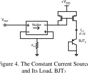
4.4 The constant and PTAT current sources
The constant current is required to biasing BJT2
in Figure 3. In order to make the current generated by the source relatively immune to the disturbance of power source, the voltage to generate the current is fed from the bandgap reference output voltage. Figure 4 shows the nullor-level block diagram of the constant current source which is a transconductance amplifier.
Figure 4. The Constant Current Source and Its Load, BJT2
For this amplifier the high-frequency instability is experienced at 2 MHz and eliminated by adding a 4 pF capacitor in series with a 20 k resistor from bandgap reference, Equation (2). From Equation (2), the constant term is:
VPTAT (Tr)= a1VBE1(Tr) +a2VBE2(Tr) (14)
the first-order temperature dependency term is:
and the second and higher-order temperature dependency terms is:
If the current biasing both BJTs has same temperature dependency, then in order to eliminate the second and higher-order temperature dependency terms:
2
1 a
a (17)
This condition changes Equation (15):
r r r PTAT ST
T T T T V T
V1 ( ) ( ) (18)
which is a PTAT voltage. Exploring Equation (14):
) (
) ( ) (
) ( ln
) (
) ( ln ) (
) ( ln )
(
2 2 1 1
2 2 2 1 1 1
r C
r S
r S
r C r
r S
r C
r S
r C r
r PTAT
T I
T I T I
T I q akT
T I
T I a T I
T I a q kT T V
(19) where a = a1 = –a2.
If BJT1 is biased with a current which is N
times the current biasing BJT2
) ( )
( 2
1 r C r
C T N I T
I (20)
and the area of BJT2 is M times the area of BJT1
) ( )
( 1
2 r S r
S T M I T
I (21)
then equation (19) becomes:
) ln( )
( N M
q akT T
V r
r
PTAT (22)
This shows that now the constant ‘a’ is not necessary to be set to a certain value. It shows also that the product of N and M have to be larger than one. If the PTAT voltage in equation (19) is across a resistor then the current flowing through the resistor is a PTAT current.
Figure 5 shows a common circuit topology to generate a PTAT current with a =1. The voltage across RPTAT is a PTAT voltage. Therefore the current through it is a PTAT current, which biases QZ. This current is mirrored by PMOS pair MY and MZ to bias QY. Therefore the biasing current of QZ and QY is of the same temperature behavior. BJT QY in Figure 5 also functions as the reference BJT1, as
in Figure 3.
RPTAT N
M
MY MZ
QY QZ
Figure 5. PTAT Current Source
For the frequency behavior analysis, it shows an instability at about 1.7 MHz which is then eliminated by putting a 4 pF capacitor in series with
a 15 kΩ resistor between the gate of MY and MZ and
the ground.
5. Simulation Results
In this paper three simulation results are represented. They are the output of the PTAT current source circuit (Figure 6), the designed reference voltage (Figure 7) and the effect of the voltage source to the reference voltage (Figure 8).
Figure 6. The Generated PTAT Current
The PTAT current source swings linearly from 5.76A at 0oC to 7.66A at 120oC or 15.83nA/K. Its
output noise level is 0.58V at 1kHz and 60oC.
Figure 7. The Output of The Simulated Bandgap Reference.
The mean temperature dependency of the output voltage is about 22.5 ppm/K, in this condition the scaling factors a1= 0.986 and a2= 0.852. Its noise level is 1.823V at 60oC and 1kHz..
Figure 8. The Bandgap Output Voltage as The Function of The Temperature for Several Level of DC Voltage Supply
6. Conclusion
In this research the design of the bandgap reference as well as a PTAT current source have been done and simulated. Due to the use of the substrate BJT, the scaling factor a1= 1 can be achieved only by a scaling circuit. Therefore, the designed bandgap reference actually has still two scaling factors.
The designed bandgap reference circuit has an output voltage of 140mV and a temperature dependency of 22.5ppm/K. Its noise level about 57.6nV/√Hz. Its total current consumption is about 115μA from a 2V voltage-supply.
References
[1] Austria Micro Systems, October 1988, 0.6um CMOS CUP Process Parameters, Document#: 9933011, Revision#: B.
[2] Austria Micro Systems, October 1988, 0.6um CMOS Design Rules, 7 Digit Document#: 9931025, Revision#: 2.0.
[3] Azarkan, van Staveren and Fruett, 2002, A Low-noise Bandgap Reference Voltage Source with Curvature Correction, IEEE International Symposium on Circuit and Systems, 26-29 May 2002. Pages: III-205 – III-208 vol.3. ISBN: 0-7803-7448-7/2. IEEE.
[4] Gilbert, B. Editors: J. H. Huijsing, R. J. van de Plassche and W. M. C. Sansen,1996, Monolithic Voltage and Current References: Theme and Variations, Analog Circuit Design, Page: 243-352. Dordrecht, The Netherlands, Kluwer.
[5] Howe, Roger T., and Sodini, Charles G., 2003, Microelectronics An Integrated Approach, Lecture 16 T-Th.
http://www.prenhall.com/howe3/microelectroni cs/html/lectures_folder/lectures-tth.html.
[6] Leach, W. Marshall Jr., 1999-2002, EE6416 Low-Noise Electronic Design, Chapter 7 Noise in Diode and BJT’s.
http://users.ece.gatech.edu/~mleach/ece6416/.
[7] Leung, Ka Nang, and Mok, Philip K.T., April 2002, A Sub-1-V 15-ppm/ C CMOS Bandgap Voltage Reference Without Requiring Low Threshold Voltage Device. IEEE Journal of Solid-State Circuits. Vol. 37. No. 4.
[8] Van Staveren, Arie, Editors: W.A. Serdijn, C.J.M Verhoeven and A.H.M., 1995, Analog IC Techniques for Low-Voltage Low-Power Electronics, Chapter 5 Integrable DC Sources and References, Delft, Delft University Press.
[9] Van Staveren, Arie, 1999, Structured Electronic Design of Bandgap References and PTAT sources in CMOS, The Netherlands, TUDelft
[10]Van Staveren, Arie, 2000, Structured Electronic Design: High Performance Harmonic Oscillator and Bandgap, Chapter 6 Bandgap References. ISBN 0-7923-7283-2, Dordrecht, Kluwer.
[11]Yuhua Cheng et al., 1996, BSIM3v3 Manual, Barkeley, Department of Electrical Engineering and Computer Science, University of California.
Attachment
The figure attached is the whole designed circuit. The supplying current sources are not shown.
![Figure 1(a)[10]second-order bandgap reference. Because constant, if the temperature dependency of the output voltage is unchanged](https://thumb-ap.123doks.com/thumbv2/123dok/1437780.1523792/1.595.90.524.609.746/figure-bandgap-reference-constant-temperature-dependency-voltage-unchanged.webp)