Nikolai Mäntyoja
School of Electrical Engineering
Thesis submitted for examination for the degree of Master of Science in Technology.
Espoo 25.01.2016
Thesis supervisor:
Prof. Mervi Paulasto-Kröckel
Thesis advisor:
Author: Nikolai Mäntyoja
Title: Evaluation of Characterization Methods for Cu-Sn Micro-Connects
Date: 25.01.2016 Language: English Number of pages: 9+105 Department of Electrical Engineering and Automation
Professorship: Electronics Integration and Reliability Supervisor: Prof. Mervi Paulasto-Kröckel
Advisor: M.Sc. Mikael Broas
The microelectronics industry constantly aspires to shrink the device features. At the package level, this implies a decrease in the interconnect size leading to small volume interconnections that are commonly called micro-connects. Smaller material volumes may give rise to new reliability challenges, such as open circuits, due to Kirkendall voiding. The root cause(s) for Kirkendall voiding is not yet clear and the methods for characterization are still varied.
This thesis reviews techniques to characterize the microstructure and impurities in Cu-Sn micro-connects. The evaluated techniques are Auger Electron Spectroscopy (AES), Electron Energy Loss Spectroscopy (EELS), Energy-Dispersive X-Ray
Spec-troscopy (EDX), X-Ray SpecSpec-troscopy (XPS), Secondary Ion Mass Spectrometry (SIMS), Rutherford Backscattering Spectrometry (RBS), Elastic Recoil Detection Analysis (EELS), Transmission Electron Microscopy (TEM), Focused Ion Beam (FIB), and Scanning Acoustic Microscopy (SAM). From the reviewed techniques, EDX, FIB, SAM, and TEM are used in the experimental section. For the first time, impurities are measured directly inside Kirkendall voids. It was discovered that the Kirkendall voids in annealed Cu-Sn samples contained a significant amount of chlorine and oxygen.
The ASTM grain size counting method was applied to FIB-polished samples. It was observed that the grain size did not increase by annealing at 150 ◦C. Furthermore, for the first time, GHz-SAM was used to characterize Kirkendall voids. The technique is promising but it is still affected by the low lateral resolution.
Tekijä: Nikolai Mäntyoja
Työn nimi: Kupari-tina mikroliitosten karakterisointimenetelmät
Päivämäärä: 25.01.2016 Kieli: Englanti Sivumäärä: 9+105 Sähkötekniikan ja automaation laitos
Professuuri: Elektroniikan integrointi ja luotettavuus Työn valvoja: Prof. Mervi Paulasto-Kröckel
Työn ohjaaja: DI Mikael Broas
Mikroelektroniikkateollisuus pyrkii jatkuvasti pienentämään laitekokoa. Paketoin-titasolla tämä tarkoittaa sitä, että sirujen välisten liitosten kokoluokka on siirty-mässä kohti mikroliitoksia, jotka saattavat aiheuttaa uusia luotettavuusongelmia. Kirkendall-aukot ovat yksi syy kyseisiin luotettavuusongelmiin ja aukkojen alkuperä on vielä tuntematon. Sen lisäksi, mikroliitosten ja Kirkendall-aukkojen karakteri-sointiin käytetään toisistaan poikkeavia menetelmiä eikä sopivista metodeista ole vielä yhteisymmärrystä.
Tämä diplomityö tarkastelee kupari-tina mikroliitoksien mikrorakenteen ja epäpuhtauksien analysointiin käytettyjä menetelmiä. Tarkasteltavat menetel-mät ovat Auger-elektronispektroskopia (AES), epäelastinen elektronisironta (EELS), energiadispersiivinen röntgenspektroskopia (EDX),
röntgenfotoelektro-nispektroskopia (XPS), sekundääri-ionimassaspektroskopia (SIMS), Rutherford-takaisinsirontaspektroskopia (RBS), rekyylispektrometria (ERDA), läpäisyelektro-nimikroskopia (TEM), keskitetty ionisuihku (FIB) ja akustinen mikroskopia (SAM). Esitellyistä menetelmistä kokeellisessa osiossa käytettiin EDX:ää, FIB:ä, SAM:a ja (S)TEM:ä. Tässä diplomityössä on mitattu ensimmäistä kertaa epäpuhtauk-sia Kirkendall-aukkojen sisältä. Mittauksista saatiin selville, että hehkutettujen kupari-tina -näytteiden Kirkendall-aukot sisälsivät huomattavan määrän happea ja klooria.
Raekokoa tarkasteltiin kiillottamalla näytteet FIB:llä ja soveltamalla ASTM:n raekoko -standardia. Työssä huomattiin, että raekoko ei kasvanut, jos näytteitä hehkutettiin 150 ◦C lämpötilassa. Tämä on myös ensimmäinen kerta, kun GHz-SAM:a on käytetty Kirkendall-aukkojen tutkimiseen. Tulokset olivat lupaavia, mutta menetelmän alhainen sivuttaissuuntainen resoluutio on vielä rajoittava tekijä.
Avainsanat: Mikroliitokset, Huokoisuus, Epäpuhtaudet, Kirkendall-aukot, TEM, FIB
Preface
This thesis is related to research by my colleague Glenn Ross, whom I would like to thank for the idea of this thesis. I also want to thank the other members of our research group for teaching me during the two and a half years that I was able to participate in fascinating research in the field of electronics reliability and integration. I particularly would like to thank my supervisor Professor Mervi-Paulasto Kröckel as well as my advisor M.Sc. Mikael Broas. My supervisor has provided me excellent guidance and possibility for flexible working conditions. My advisor provided me help by scheduling, giving excellent commentary, and assisting in grammar. I also want to thank my family and Emma for understanding the stress during the demanding task that I was occupied with. Furthermore, I would like to thank Fraunhofer IMWS for providing the (S)TEM, STEM-EDX, and GHz-SAM results for this thesis.
Otaniemi, 25.01.2016
Contents
Abstract ii
Abstract (in Finnish) iii
Preface iv
Contents v
Symbols and abbreviations vii
1 Introduction 1
2 3D Integration 2
3 Research Question 7
4 Impurity Analysis 8
4.1 Auger Electron Spectroscopy . . . 9
4.2 Electron Energy Loss Spectroscopy . . . 13
4.3 Energy-Dispersive X-Ray Spectroscopy . . . 15
4.4 X-Ray Photoelectron Spectroscopy . . . 17
4.5 Secondary Ion Mass Spectrometry . . . 19
4.6 Rutherford Backscattering Spectrometry . . . 23
4.7 Elastic Recoil Detection Analysis . . . 27
4.8 Comparison . . . 30
5 Structural Characterization 32 5.1 Grain Size Calculations . . . 32
5.2 Transmission Electron Microscopy . . . 36
5.3 Focused Ion Beam . . . 42
5.4 Scanning Acoustic Microscopy . . . 49
5.5 Comparison . . . 52
6 State of the Art in Micro-Connect Characterization 53 7 Materials and Methods 57 7.1 Sample Preparation . . . 57
7.2 Grain Revelation by FIB . . . 60
7.3 TEM Lamella Preparation . . . 61
7.4 Practical Advice for FIB Helios 600 . . . 63
8 Results and Discussion 64 8.1 Structural Analysis . . . 64
8.1.1 FIB . . . 64
8.1.3 GHz-SAM . . . 77 8.2 Impurity Analysis . . . 80 8.2.1 STEM-EDX . . . 81 9 Conclusions 86 References 88 A Appendix 102 B Appendix 103 C Appendix 105
Symbols and abbreviations
Symbols
EK Initial binding energy EL1 First outer shell energy
EL2,3 Second outer shell energy
φ Work function of the instrument hv Energy of an X-ray
EB Binding energy EK Kinetic energy
IM Total ion count of the matrix ID Total ion count of the element
N Number of grains per square inch when the magnification is 100x n Grain size number (ASTM)
NA Number of grain sections per unit test area A Mean area of the grain section
d Mean grain diameter l Mean liner intercept D Spatial diameter of sphere D0 Initial grain size
D Grain size at time t n Grain growth exponent k0 Grain growth constant
Ea Activation energy R Gas constant NT Atomic density q Electron charge YS(θ) Sputtering yield θ Incident angle
Abbreviations
3D Three dimensional ADF Annular dark field
AES Auger electron spectroscopy ALD Atomic layer deposition
ASTM American society for testing and materials BE Binding energy
BF Bright field BGA Ball grid array
BSE Back-scattered electron
CERD Coincident elastic recoil detection CMA Cylindrical mirror analyser
CMP Chemical-mechanical planarization CTE Coefficient of thermal expansion D2D Die-to-die
DOF Depth of focus
EBSD Electron backscatter diffraction
EDX Energy-dispersirve X-ray spectrometry EELS Electron energy loss spectroscopy ERDA Elastic recoild detection analysis F2B Face-to-back
F2F Face-to-face
FEG Field emission gun
FESEM Field emission scanning electron microscope FIB Focused ion beam
FWHM Full width at half maximum GIS Gas-injection system
HAADF High-angle annular dark field
HRTEM High-resolution transmission electron microscope HSA Hemispherical sector analyser
IBL Ion beam lithography IC Integrated circuit
ICP-AES Inductively coupled plasma atomic emission spectroscopy IMC Intermetallic compound
IMPF Inelastic mean free path IoT Internet of things
KE Kinetic energy KGD Known good dies
LIM Linear intercept method LMIS Liquid-metal ion source
MEMS Micro-electromechanical system NEMS Nano-electromechanical system PCB Printed circuit board
PIXE Particle-induced X-ray emission
RBS Rutherford backscattering spectrometry RSF Relative senstivity factor
RT Room temperature SAED Selected area diffraction
SAEM Scanning auger electron microscopy SAM Scanning acoustic microscope SDD Silicon drift detector
SEM Scanning electron microscope SIMS Secondary ion mass spectrometry SiP System-in-package
SLID Solid-liquid interdiffusion SoC System-on-chip
SPS Bis-(3-sulfopropyl)-disulphide
STEM Scanning transmission electron microscopy TEM Transmission electron microscopy
ToF Time-of-Flight
TRIM Transport of ions in matter TSV Through-silicon via
UBM Underbump metallization W2W Wafer-to-wafer
WLP Wafer-level packaging
The demand for reduced power consumption, higher bandwidth, and greater inter-connection density has gradually migrated the microelectronics industry towards three dimensional (3D) integrated circuits (3D ICs). Through-silicon via (TSV) has been attracting much attention as a novel technology for 3D ICs as TSV technology can reduce interconnection lengths by employing vertical electrical routing that passes through dies. [1] As it happens, 3D packaging is much more than TSVs since the interconnections between stacked wafers or dies have a crucial role as stacking multiple dies is not possible without interconnections.
In face-to-back (F2B) stacking, the interconnection pitch is limited by TSVs as the device layers are not facing each other. In the face-to-face (F2F) stacking, the bandwidth is limited by the interconnection density since the bottom device layer is facing up. Therefore, reduced pitch is one of the top requirements for 3D interconnects. [2] Alternative novel technologies have been suggested to reduce the interconnection pitch from 40 µm to sub-20 µm. Some examples of these technologies areµ-inserts,µ-tubes, and Solid-Liquid Interdiffusion (SLID) bonding. [3] These new technologies have similar reliability issues as older technologies such as microbumps. For example, it is known that Cu-Sn SLID bonds are susceptible to failures under thermal cycling (TC). The reliability issues can be assumed to be, at least partially, due to fractures initiated by Kirkendall voids [3]. However, the reliability of SLID bonds depend on the material choices since Ni-Au-Sn based SLID bonds may withstand even 3000 cycles of thermal shocking [4].
Kirkendall voids are not unique defects for only SLID bonds but a universal problem with the joining of metals with different diffusion rates. Kirkendall voids weaken the thermal, electrical, and mechanical properties of a solder joint [5]. However, due to the large volume of BGA solder joints, Kirkendall voids have not had a significant impact on reliability. The trend towards micro-connects below 10 µm has given rise to new reliability problems, for instance, in automotive applications that have to withstand varying temperatures. The general consensus regarding the root cause for Kirkendall voids is the difference of interdiffusion rates between the solder and underbump metallization (UBM). Any factors changing the rate of interdiffusion could promote Kirkendall void formation, such as electromigration and thermomigration. [5] A small fraction of researchers suggest that in the case of the Cu-Sn system, Kirkendall voiding should be renamed since it is not caused by the Kirkendall effect, but by the impurities embedded in copper from electroplating. [5–7] As the root cause for Kirkendall voiding is not yet clear, the aim of this thesis is to compare the characterization methods for micro-connects, especially from the perspective of Kirkendall voiding. The thesis introduces and compares techniques for impurity analysis and microstructural evaluation. Some of the introduced tools are used, and the results will be presented at the end of the thesis. Based on the analyzed results, there will be a discussion about which theory regarding Kirkendall voids seems strongest. The conclusion summarizes the main results of the work.
2
3D Integration
The micro- and nano-electromechanical system (MEMS/NEMS) industry benefit from advanced 3D ICs and wafer-level packaging (WLP) since the functionality of single component can be increased. Functional diversification is called "More than Moore" while conventional Moore’s law is about downscaling dimensions of ICs and memory chips. Internet of things (IoT) is one of the major driving forces for the development of 3D ICs as consumers demand more functionality packed on a smaller space.
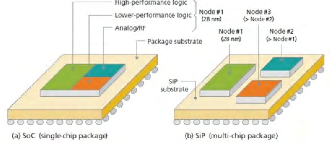
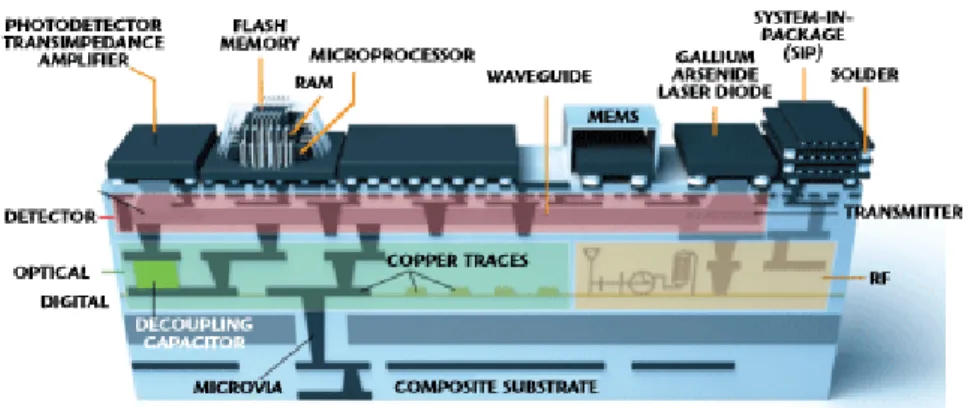
There exist various technologies which can be used to integrate diverse electronic functions into subsystems. Currently, the most used are System-on-chip (SoC) and System-in-package (SiP). SoC combines all the divergent functions into a single chip, whereas SiP combines multiple chips into a single package. The difference of SoC and SiP is shown in Figure 1. However, SiP and SoC are not mutually exclusive, but they can co-exist in the same system. Nevertheless, the functionality and performance of SoC or traditional SiP might not be enough for future applications. Since novel applications require more integration in smaller space, the electronics industry is migrating towards 3D integration with the SiP approach. The reason is that SoC causes chips to grow very large decreasing the yield. Secondly, using a single chip forces same scaling for all the function blocks even though not all have to be scaled. In contrast, each block can be scaled at a different rate with the SiP approach. The modern SiP approach for 3D ICs relies on TSVs, interposers, micro-connects, and different die stacking schemes. Ultimately, the final objective is to integrate and miniaturize all components under one system, called System-on-package (SoP) which is shown in Figure 2. [8]
Figure 1: The fundamental difference between SiP and SoC is the amout of dies. The SoC approach includes only one chip that has multiple functions and the SiP approach includes multiple dies stacked or side by side. [9]
Figure 2: The ultimate objective is to blur the limits between dies, package and the substrate. [10]
The two approaches for 3D stacking are bonding at the wafer level or at the die level. The die level bonding includes die-to-die (D2D) and die-to-wafer (D2W) bonding. Typical wafer-to-wafer (W2W) bonding uses either a oxide or metallic bond, such as direct oxide bond or SLID bond. Variations may involve the use of a polymer or adhesive to improve bond characteristics. [11]
The W2W approach requires same die sizes on both wafers and a relatively high wafer yield since the yields are multiplied when stacking multiple wafers (e.g. 0.99∗0.99∗...). Furthermore, the bonding process is sensitive to topographical
variations since the bonding area is considerably large. The final thickness of the top wafer can be in the range of 10 µm since wafers are usually thinned and the TSVs formed after bonding. Therefore, the TSV length can be minimized to 10 µm and the W2W bonding is well suited for fine pitch applications since the aspect ratio limitation of TSVs is not a concern and alignment for wafers is more accurate than with other methods. [11]
D2D bonding has lower throughput than W2W bonding but D2D is not limited by the dimensions of the die and the wafer. Furthermore, the yield is not a concern for multiple stacks since only known good dies (KGD) can be used. Also, D2D resembles a more standard chip assembly than a microfabrication technique. The TSVs are usually manufactured after bonding and due to the handling issues, the thickness of a single die is typically 50-100 µm. The TSV depth is on the same range increasing the interconnection pitch since the TSVs can be narrow. Consequently, the increased pitch limits the usage of D2D bonding for applications requiring fine pitch. An example of D2D bonded structure is shown in Figure 3. [11]
Figure 3: D2D bonding can be used to form a stack of dies connected with micro-connects. The dies are relatively thick and the pitch is limited. [11]
D2W bonding is a combination of D2D and W2W bonding. In the D2W approach, multiple dies are placed on the wafer and joined simultaneously. The throughput is high and the yield is not an issue. D2W stacking is actually more cost effective than W2W stacking and the alignment accuracy is relatively good. [8,11]
No matter what stacking scheme is used, interconnections are required between the chips. Although there exists a broad range of various platforms for 3D in-terconnections, they are all limited by the same dimension constraints, cost, and reliability requirements. Bonding interfaces are susceptible to failures as intermetallic compounds (IMCs), which may be brittle, are a large fraction of the volume, a combination of different materials cause thermal issues related to the Coefficient of Thermal Expansion (CTE) mismatch and electromigration causes new issues in the small volume interconnections [12]
The primary bonding methods are direct copper-copper bonding, eutectic bonding and soldering. One popular approach in 3D IC interconnection manufacturing is bonding by lead-free solder bumps or copper pillars that can be manufactured by conventional mass-reflow or thermocompression. The diameter of those microbumps is one order of magnitude smaller and the volume can be 1000 times smaller than that of the flip-chip solder joints. The number of grains in a single solder joint becomes small and the microstructure of the solder joint can be considered to be anisotropic. That means that properties of each microbump can be different causing a large spread in lifetime distributions. Therefore, it is desirable to have a similar microstructure in each microbump. Furthermore, the relative amount of IMC is greatly increased if parameters used in the traditional flip-chip reflow process are adopted for the microbumps. On top of that, the solder thickness has been reduced more than the thickness of the UBM. In some scenarios, the entire microbump is completely transformed into intermetallics causing new reliability problems or unexpected behaviour. [8,13]
materials for the micro-connects in 3D IC applications. The Ni diffusion layer between Cu and Sn reduces interdiffusion and formation of Sn whiskers, but it makes the micro-connect more brittle due to formed (Cu,Ni)6Sn5. In addition to
the thermocompression and the reflow process, SLID bonding is emerging as a very reliable future technology for micro-connects. SLID bonding is based on the fact that the melting point of the IMC is higher than that of the solder itself. The IMC growth is carefully controlled during the bonding process to increase the joint reliability. SLID bonding is a thermocompression type bonding process that can be done at relatively low temperatures. Therefore, the process can be repeated to stack multiple layers without remelting the lower level bonds. For these reasons SLID bonding has drawn much attention. [8,13]
free solders in combination to a copper UBM are not without problems. Pb-free solder is usually harder than eutectic Sn-Pb solder reducing the stress absorption of the solder joint. [13] Furthermore, electroplated copper contains impurities that might participate in void formation on the interface ofCu3Sn and electroplated Cu.
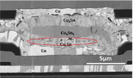
That is a real concern since one of the most important property of a solder joint is the strength. An example of a non-reliable micro-connection bonded by SLID is shown in Figure 4.
Figure 4: A micrograph of a Cu-Sn SLID bond. Kirkendall voids are visible inside Cu3Sn and between the Cu3Sn and Cu. The voids decrease the strength of the joint
and might cause electrical failures. [3]
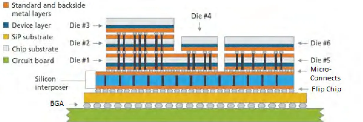
Ball Grid Array (BGA) solder joints and flip-chip technologies are not yet obsolete. BGA is used for connections between the package substrate and printed circuit board (PCB), and the flip-chip is used between the interposer and the substrate. However, the size of the solderbumps between the interposer and the substrate is decreasing towards the size of the micro-connects. The different interconnection levels are shown in Figure 5.
Figure 5: The package contains different level interconnections. BGA solder joints are used between the PCB and substrate, flip-chip between the substrate and interposer and micro-connects between the dies. [14]
3
Research Question
The impact of Kirkendall voids on the reliability and mechanical properties will become even more critical in the micro-connects. The reason is that the size of Kirkendall voids can be a large fraction of the volume of a micro-connect itself. The focus of this thesis is in the micro-connects, especially in characterization methods related to Kirkendall void research. It is known that several factors influence Kirkendall voiding such as impurities, grain size, film thickness, additional layers, and electroplating parameters. [3,5,7]
Furthermore, it has been shown that post-deposition annealing suppresses Kirk-endall voiding formation due to outgassing of organic impurities [15,16]. That gives even more proof that the voiding effect is not due to the Kirkendall effect but due to organic impurities. However, the main culprit has been usually claimed to be sulphur content [15,17–20], but there is not yet strong evidence to support this conclusion. The relation between electroplating bath chemistry and Kirkendall voiding is compli-cated. The known fact is that the organic additive molecules and their derivatives can be incorporated into the metal film during the electroplating. Furthermore, it has been shown that different additives, current density, and age of the plating bath can directly affect the voiding propensity individually. [20]
Sulfide-forming elements such as Zn, Mn and Cr are shown to suppress Kirkendall voiding due to suppression of S adsorption on the void surface [19]. However, that claim might be questionable due to insufficient chemical analysis and lack of consideration of other impurities that may participate, such as O, C, and Cl. Similar to the S, the Cl may form chlorides with those sulfide-forming elements.
Since it is not clear which factors are dominant, several characterization methods are required to study Kirkendall voids and the root cause(s) for their growth. It is not enough to understand just the characterization methods, but to study the micro-connects and their manufacturing methods as a whole. The main question is that why Kirkendall voids form? Research is required to obtain the answer and for that different characterization techniques are required. Testing and a comparison of different techniques is time-consuming; thus there is a need for comparison of characterization methods. This thesis compares different characterization methods related to micro-connects and Kirkendall voids from the standpoint of limitations, ease of use, quality of data and time efficiency. Since there should be a link between impurities and Kirkendall voids, the most important techniques are related to impurity analysis and structural analysis.
4
Impurity Analysis
Currently used electroplating methods do not produce pure copper, as seen in Table 1. The table shows impurity measurements in at.% for electroplated copper from various references. However, Table 1 is not precise as some of the results had to be interpreted from graphs or the total copper amount was calculated based on the total amount of impurities. Secondly, some of the results were not used for calculation of the average since they seemed not to be reliable. Additionally, results that contained an excess amount of carbon and oxygen were discarded since the measurement or deposition is not probably successful. The depositions with a high level of Zn should also be discarded since the copper electrolytes do not contain Zn. Table 1 suggests that electroplating incorporates at least carbon, oxygen and nitrogen in the films. Additionally, for the electroplated copper, most of the concerns rise from the Cl and S concentration. If more additives are used in the bath chemistry, there are more different contaminants in the copper film. However, that does not necessarily mean that the total amount of impurities is higher.
Table 1: Tabulated impurity measurements in at.% for electroplated copper from various references. Concentration data showing less than 85 at.% Cu were omitted in the literature review.
Tool Cu(%) O(%) C(%) Cl(%) Zn(%) S(%) Ref. EDX 85.00 1.00 7.00 − 7.00 − [21] EDX 89.00 2.00 5.00 − 4.00 − [21] SIMS 87.10 7.30 5.60 − − − [22] SIMS 99.90 0.01 0.02 0.05 − 0.005 [23] SIMS 94.60 2.20 1.80 1.30 − 0.10 [24] SIMS 97.40 1.00 1.00 0.50 − 0.10 [25] Average 92.20 2.20 3.40 0.60 0.10
As seen in Table 1, the impurities in electroplated copper are usually measured by secondary ion mass spectrometry (SIMS) or energy-dispersive X-ray spectrometry (EDX). Unfortunately, EDX is not a reliable technique for lighter elements which is discussed in Section 4.3. The unreliability of EDX for impurity analysis is confirmed by C-H. Liao [21] by X-ray photoelectron spectroscopy (XPS) measurements that showed copper purities over 90 at.%, whereas EDX measurements for the same samples showed copper purities of 85-89 at.%. The SIMS analysis by D.L. Malm and M.J. Vasile [22] were done for surface-etched samples. The etching removed contaminants, such as Cl and S. Without etching, the copper surface contained∼3
at.% Cl and S. Additionally, the surface etching did not decrease the amount of O, but the amount of C was drastically decreased. The measurements by K. Denn et al. [26] confirm that the impurities such as Cl and S are mostly located on the surface of the copper and not in the bulk. However, the initial location of the impurities is not yet clear since impurities could diffuse to the surface during even a short storing time at the room temperature. The measurements by Q. Huang et al. [23] differ greatly from the other results since all their measured impurities are in a ppm range.
Therefore, the results should be treated with caution. In conclusion, purity of 90 at.% could be considered a good standard for quality electroplated copper. Additionally, depending on the measurement and bath chemistry, the electroplated copper will probably contain∼2 at.% C,∼3 at.% O, and less than 1 at.% Cl and S. This section
reviews popular and less known tools for impurity analysis. The reviewed tools were chosen by the ability to locate the impurities in a specimen and by the ability to analyse solid samples. The section is finalized by a comparison that attempts to evaluate the best choice among the reviewed tools.
4.1
Auger Electron Spectroscopy
The Auger effect was discovered by Pierre Auger in 1923, but the first commercial Auger electron spectroscopy (AES) instruments were introduced in the late 1960s. [27] AES analyses the kinematic energy of Auger electrons which are ejected when a system with an electron vacancy relaxes. The vacancies are usually produced by 5-25 keV electron beam by ejecting an electron from an inner K-shell. [27,28] The process can be written as a simplified equation:
E =EK−EL1−EL2,3−φ, (1)
,where EK is the initial binding energy, EL1 first outer shell energy,EL2,3 second
outer shell energy, andφthe work function of the instrument. The equation resembles that of XPS. However, the equation is a simplified expression due to transition probabilities between double ionized states, multiple excitations and Coster-Kronig transitions. The measured kinetic energy is usually in the range of 50-2500 eV. [27] An example of the transition is shown in Figure 6 [29].
Figure 6: An electron is removed from the K-shell by the electron beam and the vacancy is filled by an electron from an upper shell. To balance the upper shell, an Auger electron is emitted from the same shell from where the electron was relaxed. [29]
The Auger transition is characterized by the presence of the core hole and location of the two final states. [29] AES instrument consists of an electron gun, an ultra high vacuum chamber and an electron detector. [27] The electron source is similar type than in scanning electron microscope (SEM) such as field emission gun or thermionic tungsten source. The detector is usually either cylindrical mirror analyser (CMA) or hemispherical sector analyser (HSA).
AES can refer to a conventional point analysis technique, or a scanning technique called scanning auger microscopy (SAEM) that is analogous to SEM. Furthermore, SEM-EDX and SAEM has similar scanning speeds to acquire elemental maps. Similar to SEM-EDX, SAEM can be used to scan line and mapping profiles. The major difference between SEM-EDX and AES is the interaction volume since the Auger electrons are emitted from the surface. Generally, SAEM uses a smaller beam diameter than the point analysis AES. However, the scanning mode is not acquired without disadvantages. The change of slope during the scanning changes the detected intensities and the background intensity, especially if the incident beam size is small. However, the most drastic intensity changes can be corrected using BSE detectors. Secondly, it is challenging to use scanning mode for structures that have sharp edges or wells that will cause shadowing and trapping of Auger electrons. Moreover, typical SAEM instrument has a beam size of 10-20 nm that can detect a few hundred atoms simultaneously. The spatial resolution limitations are mainly caused by radiation
damage and topographical effects. [27]
The major advantage of AES is the extreme surface sensitivity that is similar to XPS. The surface sensitivity emerges from the 0.3-3 nm inelastic mean free path (IMPF) of electrons. The IMPF depends on the electron kinetic energy (composition)
and incident electron energy. [27] AES is a three electron process, whereas XPS is one electron process. In that sense, XPS peaks are easier to fit. Furthermore, since at least three electrons are required for the Auger process, AES is not compatible with elements Z < 3. In addition, unwanted inelastic collisions produce low energy backscattered electrons that contribute to the AES spectrum and they are regarded as background intensity or noise. Therefore, the Auger spectrum contains a high amount of unwanted noise that should be eliminated by the peak fitting. An example of AES spectrum is shown in Figure 7. [29]
Figure 7: The Auger electron peaks are only a small part of the spectrum. The spectrum is dominated by noise from the backscattered electrons. The elastic peak is caused by the electron beam and it is used for calibration. The loss peaks near the elastic peak are related to ionization levels. However, the spectra do not contain photoemission peaks. [29]
The probability of creating core-hole electron depends on the e-beam energy and core hole binding energy. The rule of thumb is that the maximum probability is reached when the incident beam energy is three times higher than the core hole binding energy. However, the probability is different for different elements. For example, Auger process in light elements is very probable in contrast to X-ray emission as seen in Figure 8. [29]
Figure 8: The yield per shell vacancy of X-rays (X) and Auger electrons (A) in relation to atomic mass number. The probability for Auger electron emission is relatively good for a whole range of elements. As can be seen, the probability for X-ray emission in light elements is low and that causes problems when EDX is used. [29]
AES can be used to acquire different types of spectra. The most popular ones are the first derivatives of the electron energy distribution since the chemical shifts and spectral quantification are simple to analyse in the derivative mode. Although, the derivatives are restricted to samples that do not cause a change in the peak shape. However, the derivative spectra are not necessarily comparable to spectra acquired by other AES tools. These disadvantages can be minimized if a direct spectral mode is used. The direct spectral mode acquires spectra using an incident beam in a nanoamp range and the Auger peak intensity is directly related to the chemical composition when the background noise is removed. [27]
Similar to XPS, AES can be used for probing the electronic structure. The transitions are mainly ionization of a core level followed by decay from the valence band. These shifts can be used to identify different chemical states of an atom, but they might introduce a systematic error in the results if the derivative mode is used. Nevertheless, due to the three electron process, the data is more difficult to handle and fit than with XPS and the results are not directly comparable. [27] Therefore, AES is usually used for purely atomic identification since the chemical shifts are complex.
Doing depth profiling by AES is possible. The maximum depth for electron transmission is three times the wavelength. For example, if the incident electron energy is 500 eV, the maximum depth is ∼7.5 nm. This approach requires tilting
the specimen in various angles and it is widely used with XPS, but that will not give reliable results with AES since the backscattering factor will change. To increase the analyzed depth, there is need to use a destructive method, such as sputtering byAr+
ions. The most important parameters that influence the depth resolution during the sputtering are atomic mixing, surface roughness, and sputtering depth. [30,31]
The charging shifts and distorts the acquired spectrum. However, thin dielectric layers can be investigated if the substrate is conductive due to the low voltage drop between the vacuum/dielectric and dielectric/substrate interfaces. Furthermore, electron beam might damage sensitive samples similar to SEM. [27]
Auger peaks are generally broader than XPS peaks. Therefore, the analyzer can be lower resolution and angular collection efficiency is not a problem. In addition, AES is faster than XPS, but misuse of relativity sensitivity factors might produce a big error in the results. The lateral resolution of AES is 10-100 nm and detection limit is 0.1 at.% [30] However, there is a trade-off between lateral resolution and capability for quantification. Improved lateral resolution requires a smaller incident beam that is consequently weaker decreasing the signal-to-noise ratio. Since the beam diameter is smaller, the acquisition speed has to be increased to keep the measurement time reasonable. These properties hinder the capability for accurate quantification if the tool is set to improved lateral resolution. [27] The quantification should be improved further by using a reference library of intensities corresponding to elemental concentrations at the surface. [27] Furthermore, AES requires a smooth surface and in the best-case scenario, the sample would be amorphous since quantitative analysis suffer from the channelling effect in the crystalline samples. [27]
4.2
Electron Energy Loss Spectroscopy
Electron energy loss spectroscopy is used to study chemical, physical, and optical properties of the materials and it is usually integrated with (scanning) transmission electron microscope ((S)TEM). In contrast to (S)TEM imaging, EELS is based on detecting inelastically scattered electrons. The energy loss due to the inelastic scattering is specific to each bonding state of each element. The method is suitable to extract information about composition and bonding. The acquired spectrum consists of zero-loss, low-loss, and core-loss regions as shown in Figure 9.
Figure 9: The spectrum is divided into three parts. The zero-loss peak is the reference energy, the low-loss peak is characteristic to the optical properties, and the core-loss region is used for elemental analysis. [32]
The zero-loss peak is used as a zero reference energy since it is the signature peak for all the electrons that have elastically passed through the sample. The low-loss region is characteristic to the optical properties of the sample and it can be separated into bulk and boundary groups. The bulk group consists of optical gap transitions, such as bulk plasmons and semi-core losses. The boundary group consists off the surface (plasmon) and Begrenzung effects. Altogether, the low-loss region can be used to evaluate the optical properties of the sample. [32]
The core-loss region typically exists beyond 100 eV and it is usually independent on the boundary effects. The core-loss signal can be used to interpret electronic transitions. The transition energy is close to the ionization energy with an accuracy of a few electron volts. The area under the edge corresponds to the amount of detected atoms if the geometrical conditions are known. The electronic structure is derived from the region near the edges since it contains information about the electronic structure, bonding, and valence. Furthermore, the spectrum can be used to calibrate energy filters for energy filtered (S)TEM imaging. [32]
EELS spectrometer is usually a magnetic prism that disperses the inelastically scattered electrons as a function of energy, but it does not change the electron trajectory. In addition to a spectrometer, EELS uses a lens system to align and focus the spectrum in the detector plane causing some energy loss. However, EELS requires a high brightness electron source such as cold FEG and the required sample thickness (usually ∼50 nm) depends on the analyzed materials. [32]
4.3
Energy-Dispersive X-Ray Spectroscopy
EDX is a technique for chemical characterization of a sample. Commonly, EDX is integrated with SEM and it is used as a chemical analysis technique while SEM is used for structural characterization. EDX relies on the interactions between the electron beam and the specimen which emits characteristic X-rays in response to the electron beam. An electron from an inner shell is excited by an electron beam producing a vacancy and the vacancy is subsequently filled by an electron from the outer shell and an X-ray is emitted. The characteristic transitions are named according to the shell in which the electron is ejected and the shell from which electron is relaxed. For example, if electron drops from L-shell to K-shell, a Kα X-ray is emitted. [33] The number and energy of the X-rays are measured by an energy dispersive spectrometer. However, to accurately measure the material, all detectable transitions should be present in the spectrum.
Continuum (Bremsstrahlung) background noise is generated by the interaction between the e-beam and atom nucleus in addition to the characteristic X-rays. The distribution of continuum X-rays is not characteristic to the material and it is considered as a nuisance. Since the probability of electron beam reaching the nuclei of lighter atoms is high, more background noise is generated by lighter elements than by heavy elements. The electron beam energy should be over critical excitation energy to ionize an atom. Besides, inner shells have lower binding energy than the outer shell and each shell has its own binding energy that has to be exceeded. However, the difference in the energy is higher in transitions between inner shells than transitions between inner and outer shells. [33]
Usually, EDX uses Si(Li) detectors that convert the energy of each X-ray to a voltage by ionizing atoms in the silicon. To increase the signal-to-noise ratio, the detector is usually cooled by liquid nitrogen and the accumulated charge is periodically restored to prevent saturation. However, the detector causes peak broadening due to its response function, peak distortion due to trapping, escape X-rays, and sum peaks due to pulse pileup. However, new silicon drift detectors (SDD) have emerged which do not require cooling while offering superior performance. [34]
The detector itself is not the main reason for inaccuracy or inability to detect light elements. The inherent problems are related to the generation of X-rays and high interaction volume. EDX is not a surface characterization technique, but it gives an average composition based on the volume of the penetrated electrons that is approximately 1 µm deep and wide as seen in Figure 10. In addition to the high interaction volume, the X-ray emission in light elements is dominated by Auger emission that is used by AES. Furthermore, X-rays generated in lighter elements are easily absorbed since they are weak. Due to the absorption, the information is mostly acquired from the surface which is especially problematic if the surface is contaminated. Moreover, reliable analysis requires acquiring all possible transitions that might overlap in the spectrum reducing the possibilities for quantification. [33]
Figure 10: The accuracy of SEM-EDX is low since the interaction volume is high. If (S)TEM-EDX is used, the interaction volume is determined by the sample thickness
and electron beam size. [32]
To provide best conditions for the EDX analysis, the sample should have flat surface, the acceleration voltage should be high enough, there should be no surface contaminations, and the material should be homogeneous. Although, even the best conditions do not provide real quantitative analysis since the data should be handled by a correction matrix that takes into account lost energy due to penetration, absorption of the X-rays, and secondary fluorescence. If the correction parameters cannot be used, at least the prefabricated profiles in the measurement software should be tested. [35]
EDX offers a possibility to carry out spot analysis, line analysis, and chemical mapping. However, the detection limit is approximately 0.1-1 at.% depending on the sample type. The spatial resolution is ∼1 µm for heavy elements and ∼5 µm for light elements. The inaccuracy between repeated measurements is less than 5 %. Reliable information of the chemical composition can be acquired if the elements are heavier than Z > 3-11 depending on the used tool. [33]
EDX is quick, versatile, and widely available. For these reasons, it is especially suitable for qualitative analysis. However, due to the reviewed limitations, the tool cannot be used for depth profiling or trace element analysis and the accuracy is reasonably low for lighter elements. If the analysed area is small and there is a possibility for lamella preparation, (S)TEM-EDX should be used instead.
EDX analysis in (S)TEM is a reliable approach to characterize materials, especially for heavier elements (Z > 30). The spatial resolution in (S)TEM-EDX is determined by incident probe size since the interaction volume is directly proportional to the probe size as shown in Figure 10. However, detection of the generated X-rays is drastically less efficient than detection of energy-loss electrons since the generated X-rays are emitted all around the sample but they are detected only with a few detectors depending on the configuration. Elemental mapping is possible with EDX,
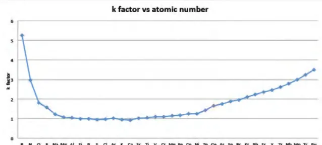
but it is moderately slow since the X-ray maps need to be recorded by pixel at a time for a long dwell time due to the inefficient X-ray generation and detection. [32] The corrections used in quantitative SEM-EDX do not apply to (S)TEM since the peak intensities are proportional to concentration and specimen thickness that can be presented as a k-factor which is an efficiency curve of the system. An example of (S)TEM-EDX k-factor curve is shown in Figure 11. However, if the sample thickness exceeds 100 nm, density and thickness corrections should be applied to acquire quantitative data. [34]
Figure 11: The k-curve shows a low efficiency for light and very heavy elements that is typical for EDX analysis. [34]
4.4
X-Ray Photoelectron Spectroscopy
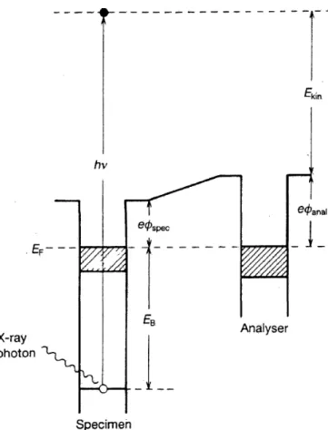
XPS is probably one of the most used surface analysis technique. It can determine the surface composition and chemical states quantitatively. [31] Experiments that used X-Rays to obtain photoelectrons were reported as early as 1907 [27]. The analysed electrons are ejected from the sample as a result of a photoemission process. Most of the electrons are emitted from the top layer (∼3nm) due to short mean free path of
electrons. Typically, anAl−Kα or M g−Kα primary source is used to generate an X-ray photon that ejects an electron from an inner electron shell of an atom. [30] The kinetic energy (KE) of the ejected electron is measured to obtain a spectrum and the ejection process can be described as:
EK =hv−EB−φ, (2)
where hv is the energy of the X-ray, EB is the binding energy (BE) with respect to the Fermi level, and φ is the work function of the tool. In other words, the photoemission is a one electron process and which is illustrated in Figure 12. The binding energy can be approximated as an orbital energy and different orbitals give different peaks in the spectrum and the peak intensity depends on the probability
for ionization. Since the core-level binding energies are unique, they can be used as a signature for different elements. However, the spectrum contains extra peaks due to the Auger emission, surface/bulk plasmons, and shake-off events.
XPS can be used to detect chemical shifts that can be described as an addi-tion/deletion of valence electrons that increase/decrease the binding energy. However, the chemical shifting involves more complex effects such as spin-orbit splitting and the Auger electron emission. Analogous to AES, the spectrum contains background noise that is generated by inelastic scattering. [36]
Figure 12: An X-ray photon excites an electron from a core-level. The kinetic energy depends on the X-ray photon energy, binding energy and work function of the tool. [36]
XPS is operated in a high vacuum and the tool consists of an X-ray source, a camera, a lens system, an energy analyzer, and a detector (HSA or CMA). The best energy resolution achieved is approximately 0.28 eV if a monochromator is used. However, there is always a trade-off between energy resolution and sensitivity. [36] Quantitative XPS analysis requires peak fitting and tables of sensitivity factors. Moreover, there exists several different software packages for XPS data handling and peak fitting. Unfortunately, different software might produce different results and accuracies. The vertical alignment of the sample is critical in some commercial instruments since misalignment of 0.1 mm might cause a 10 % error in the spectrum. In addition, the scale of the spectrum should be carefully calibrated so that the scale
differs less than 0.2 eV from the accepted values. The scale can be calibrated by an X-ray source and fitting by a quadratic equation. [31]
Similar to AES, XPS can be used for non-destructive depth-profiling for a maxi-mum depth of three wavelengths. For deeper depth profiles, destructive sputtering is required. Typically used ions are 1-10 keV Ar+-ions. During depth profiling, the
analysis spot should be at the center of the ion beam and the ion beam should be kept constant. Granted, surface roughness and the channeling effect in polycrystalline materials decrease the depth resolution. Furthermore, the sputtering might cause atomic mixing, decomposition and segregation. Similar to SIMS sputtering, the depth profile resolution can be increased by sample rotation or multiple ion beams. [36]
The greatest disadvantage of XPS is the low lateral resolution that is usually in the range of tens ofµms. However, the lateral resolution can be increased using a higher X-ray flux by a synchrotron or an X-ray laser. [30,36] Similar to AES, XPS charges the surface of the sample causing broadening of the peaks. However, the charging is not as severe as with AES and it can be taken into account while fitting the peaks or the charge can be compensated by low energy electron/ion gun. [36]
4.5
Secondary Ion Mass Spectrometry
SIMS is a technique to obtain information about the molecular, elemental, and isotopic composition of the specimen. The sample is bombarded with primary ions resulting in the ejection of the secondary ions from the surface of the sample. Typically, the secondary ions are measured with a mass analyser that produces a mass spectrum with a sensitivity of ppm/ppb. [37] The phenomenon of secondary ion emission had been discovered already in 1915, however, the first SIMS prototypes emerged in the 1940s. [38]
Similar to the focused ion beam (FIB) (reviewed in section 5.3), the sputtering is caused by collision cascade that is based on a momentum transfer between the primary ions and the surface atoms. Likewise to FIB, the ion beam causes surface damage and implantation of the sample. The depth of damaged surface might be in tens of nanometers. However, the major part of secondary ions originates from a depth of 3-6 Å. [38,39] Additionally, SIMS allows chemical mapping of the surface. [38]
SIMS can be operated either in dynamic or static mode. In the dynamic mode, the acceleration voltage and the current density are high. Due to that, the dynamic mode is suitable for high sensitivity depth profiling. On the other hand, the dynamic mode causes more damage and the spatial resolution is reduced due to the increased beam size. Sputtering rate varies from 0.1 to 100 nm/min depending on the primary ion energy, current density, type of primary ions and the angle of the incidence beam. The depth resolution can be increased by using raster-scanning. [38] An example of SIMS depth profile can be seen in Figure 13. SIMS is capable of identifying all elements in the periodic table, including hydrogen. However, the tool is most sensitive for alkali metals, halogens and oxygen and least sensitive for noble metals. [38] The dynamic SIMS is more sensitive (ppb) than static SIMS (ppm) due to the higher acceleration voltage.
Figure 13: An example of SIMS depth profile of Cr/Ni thin-film stack with nominal thicknesses of 53 and 66 nm. The sharp transition between materials indicates a successful depth profile. An unsuccessful depth profile spectrum would have empty spacings between the transitions. [37]
The static SIMS mode allows non-destructive analysis of the surface layer due to low acceleration voltage and current density. The primary ion beam does not strike the same area twice and the spatial resolution is increased [38]. Furthermore, the total ion dosage is kept under the critical (static) limit and the method is especially suitable for sensitive samples, such as polymers and biological materials. [37]
SIMS instrument consists of an ion gun, a primary ion column, a vacuum chamber with a sample holder, a secondary ion extraction lens, and a mass analyzer that measures mass-to-charge ratio of the secondary ions. The vacuum pressure of10−5
Pa is enough for dynamic SIMS, but the static SIMS requires vacuum pressure over 10−8 Pa. [38] An example of SIMS instrument is shown in Figure 14.
Figure 14: SIMS instrument consists of an ion gun, a primary ion column, vacuum chamber with a sample holder, the secondary ion extraction lens, and a mass analyzer. If the instrument does not use a time-of-flight detector, the amount of different ions detected depends on the amount of the detectors. [40]
Three basic types of mass analyzers are a magnetic sector field, a quadrupole, and a Time-of-Flight (ToF) analyzers. The magnetic sector field analyzer separates the masses by electrostatic and magnetic forces, the quadrupole by resonant electric field and the ToF by the secondary ion velocities. ToF is the only type of analyzer that can detect the whole range of secondary ions simultaneously. All the other analyzer types
require choosing of a specific range of ions to be measured. [38] Modern equipment has, at least, four different secondary ion detectors: an electron multiplier, a Faraday cup, an image plate, and an anode encoder. Some tools might have even 11 different detectors. However, it should be taken into account that not all detectors can be used simultaneously. [41,42]
ToF analyzer can be used only with static SIMS and it further reduces the surface damage. ToF-SIMS usually uses a pulsed cluster (polyatomic) ion source that is especially recommended for surface analysis of organic materials. Cluster ion beam reduces penetration depth but increases sputtering yield. Thus, the usage of cluster ions improves the quality of the SIMS depth profile for organic materials. Although, ToF-SIMS suffers from a low spatial resolution since the beam pulses are compressed to increase the mass resolution. [40]
The choice for the primary ion type depends on the investigated sample. A typical SIMS instrument usually has at least two different ion sources. [40] For larger organic molecules, large inert ions such asAr+, Xe+ orKr+ are used. Typical ion
cluster sources are C60+,Bi+23 or Bi+3. For electropositive specimens, oxygen ions are used, whereas for electronegative elements Cs+, Ga+ or In+ are used. For example,
a typical SIMS equipment for metal depth profiling could use Cs+ and O−
2 sources.
TheCs+ ions will reduce the work function of the specimen surface causing emission
of negative secondary ions. In contrast, the O2− primary ions form metal-oxygen bonds with surface atoms. During sputtering, such bonds will be broken and the emitted secondary ions will be positive. [38,40]
The ion counts from the spectra can be converted to concentrations if the relative sensitivity factors (RSF) are known [43] :
RSF =D∗ IM
ID
, (3)
where D is the concentration of the element, IM total ion count of the matrix, and ID total ion count of the element. The RSF-values for different matrices and elements can be found from the literature.
The determination of elemental concentration in the specimen is a difficult task. The ionization probability depends on the nature of the analyzed element, the sample matrix, the chemical state of the surface, and the type of primary ions used. Therefore, SIMS is usually classified as a semiquantitative method. The elemental concentration is derived from comparative measurements between the sample and known standard samples whose composition closely resembles that of the specimen. [38]
A rough surface produces artifacts in the depth profile due to preferential sput-tering (distorted secondary ion yield). The same effect can be seen in metallic materials since the sputtering yield depends on the surface orientation. Generally speaking, monocrystalline or amorphous single phase and smooth surfaces that tend to amorphize during sputtering produce the most accurate depth profiles. In contrast, polycrystalline metallic materials have the most inaccurate depth profiles. Moreover, defects such as dislocations and stacking faults might change the sputtering yield and the depth resolution decreases when the sputtering depth is increased. RMS roughness of tens of nanometers might be acceptable, but the desired roughness
is in the range of a few nanometers. The surface roughness can be polished, for example, by wet etching, chemical-mechanical planarization (CMP) or low energy ion bombardment. If polishing is not possible, the artifacts can be minimized using sample rotation during measurement or dual ion beam system that has two ion guns at different incident angles. [44,45]
Several shortcomings prevent SIMS being used as routinely as XPS for chemical analysis. For example, there is no solid theoretical foundation for the cascade collision phenomenon. Additionally, the matrix has a very strong effect on the intensity and shape of the spectra (Matrix effect) and the data handling is challenging. [38]
4.6
Rutherford Backscattering Spectrometry
Rutherford backscattering spectrometry (RBS) is based on elastic recoil collisions. Alpha particles (He+ or He2+) with an energy of 500 keV - 4 MeV penetrate the
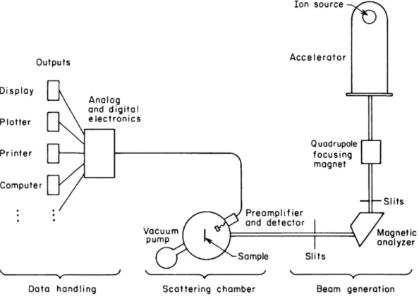
sample and backscatter due to the elastic recoils. Incident beam angle is close to the normal and only a small fraction of incident ions will backscatter. If the energy would be much lower than 500 keV, the probability for backscattering would decrease drastically. The backscattered ion energy depends on the depth and mass of the atom that caused the recoil. [46,47] RBS has long been used by nuclear physicists for a quick examination of target purity and thickness but, nowadays RBS is employed in a number of different fields. The tool is illustrated in Figure 15. [47]
Figure 15: The incident ion beam energy is carefully measured since the incident energy is used as reference for data analysis. The scattering chamber is under moderate vacuum and the chamber contains multiple detectors in different angles. [48]
A common choice for ion source is a Van de Graff generator integrated with a particle accelerator. Silicon detectors at various angles count the number of scattered particles and their energies. The interpreted information contains data of composition, distribution of elements, and sample thickness. Typically, no heavier thanHe2+ ions are used since heavier ions would cause more surface damage and decrease the energy resolution of the silicon detectors. Usually, it is a good practice to acquire data at least from three different scattering angles. [47] The probability of scattering depends on the scattering cross-section which is defined as an amount of particles that will scatter into the differential solid angle dΩ. In other words, the scattered particle can scatter to different directions from the scattering center and there is a finite probability of scattering from a target nucleus. For RBS, the scattering cross-section is fairly small since the probability of backscattering is low. [49] The scattering in RBS is demonstrated in Figure 16.
Figure 16: The incident ion beam is normal to the sample and there are different probabilities for scattering to occur in different directions. The backscattering probability is low for RBS and the probability can be modeled as a differential cross-section which depends on the scattering angle Θ, differential solid angle dΩ, and impact parameter b that is defined as a distance between the scattering center and scattering cross-section. [47]
Elements lighter than the matrix are hard to detect using RBS. Furthermore, RBS is nearly blind to carbon, nitrogen and oxygen due to the low backscattering probability, and the incident ion energy is considerably low when then incident ion is backscattered from a light element. [50] Additionally, lighter element peaks in a spectrum tend to shrink if the sample contains even thin layers of heavier elements as seen in Figure 17.
Figure 17: RBS suffers from masking by heavy elements. In this case, the Si substrate is covered by thin layers of Ta and Cu that are heavier elements than Si. The yield for the Si is not accurate. Likewise, if the sample matrix consists of heavy elements, the impurity profile for lighter elements will be inaccurate. [46]
A typical resolution limit is 0.5 at.% for lighter elements and ∼ppm for heavy
elements. [46] The major disadvantage of RBS is that two elements of similar mass cannot be distinguished. [48] That disadvantage is highlighted for heavier atoms since the incident ions transfer less momentum to heavier atoms. The atomic mass resolution in relation to the atomic weight is plotted in Figure 18. [49]
Figure 18: The mass resolution is low for heavy elements. RBS cannot differentiate heavy elements if their mass is not atleast 10 amu apart. [47]
The mass resolution for heavy atoms can be increased by using increased beam energy or using heavier incident beam ions. [47] Likewise, the resolution limit for lighter elements can be increased by increasing the incident ion energy and scattering angle. If the ion energy and scattering angle are high enough, the scattering cross-section becomes non-Rutherford and the traditional equations will not apply. Additionally, current equipment can use forward scattered particles to increase the resolution. [49] RBS can be used for depth profiling with a resolution of 5-50 nm. The depth profiling does not destroy the sample and the achievable measurement depth is usually between 1-20 µm. [48, 49] Most of the scattering occurs at a deeper level below the surface where the energy of the projectiles is decreased. The penetrated ions slow down in the sample and the beam energy is spread due to the transfer of energy to electrons or nuclei. This phenomenon is called straggling. Therefore, near the surface the resolution is highest and the resolution decreases in the deeper regions. Practically, the straggling effect depends on the stopping power of different elements. One example of straggling is shown in Figure 17. On the other hand, the film thickness can be calculated by using energy difference of scattered ions from different depths. Although, the film thickness calculations require well-defined energies of particles regarding the depth. [47]
RBS requires a low surface roughness, similar to SIMS. Very often, a spectrum that shows diffusion or mixing of elements is actually a result of the surface roughness. Therefore, quantitative RBS analysis is usually limited to laterally homogeneous and smooth films. [44, 51] Three-axis sample holder can be used to find low index crystallographic directions by monitoring RBS yield when tilting the sample [49]. Furthermore, the ion channelling effect can be used to locate lattice positions of impurity atoms in a single crystal and usage the major crystallographic directions minimizes the background noise. [47]
4.7
Elastic Recoil Detection Analysis
In contrast to RBS, Elastic Recoil Detection Analysis (ERDA) is based on elastic recoil collisions. Furthermore, RBS detects only backscattered primary ions, whereas ERDA can detect recoiled target atoms. [50] The main advantage of ERDA is its almost equal sensitivity for heavy and light elements. ERDA was first time used in 1976 by L’Ecuyer. [52] It could be said that RBS and ERDA are complementary techniques since RBS is more sensitive for elements that have a larger mass than that of the matrix, whereas ERDA is more sensitive for elements that have a lower mass than the matrix. [50]
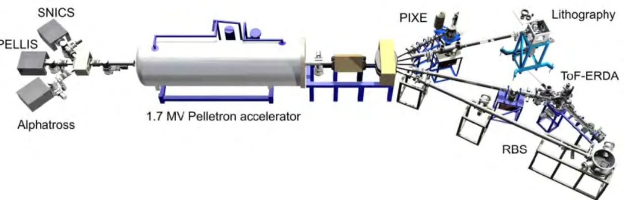
ERDA uses heavy primary ions from C to Au with an energy of several hundred MeVs that enables investigation of light elements. The most used primary ions are Cl, Cu, Br, I, and Au. [53] Furthermore, an absorber foil is usually placed in front of silicon detectors to protect the detector and stop the heaviest particles. Therefore, lighter ions will pass the foil and can be detected without masking by the heavy particles. In the optimal situation, the primary ions have approximately same mass than the atoms in the matrix. [50,53] As a tool, ERDA and RBS are very similar. Essentially, RBS can be used as ERDA if absorber foil is used and the incident ions can be changed to heavier ones. [50] Figure 19 shows a solution from University of Jyväskylä that uses same ion accelerator for RBS, ERDA, particle-induced X-ray emission (PIXE), and ion beam lithography (IBL).
Figure 19: The ion sources are different but the same ion accelerator can be used for RBS, ERDA, PIXE, and IBL. [52]
ERDA is a real quantitative method and interpreting of the spectrum does not require heavy computations or simulations. In the spectrum, the peak area represents the density of the analysed atoms in the film. The peak height indicates the concentration of that particular element. If all elements in the sample do not contribute to the spectrum, the peak can be used to calculate relative concentrations. The accurate sampling depth is less than for RBS but the resolution is at least 0.1 at.%. ERDA is suitable for thin-film analysis, especially if time-of-flight (ToF) detector is used. [50]
Analogous to RBS, the ions can be generated by a Van de Graff generator. Typical accelerators are cyclotrons or tandem accelerators. Similar silicon detectors than in
RBS can be used, but the resolution is not good for heavy ions and the silicon gets easily damaged. Furthermore, since the foil is usually used, electrons lose energy due to the straggling effect in the foil. Therefore, silicon detectors are not most suitable for accurate depth profiling. ERDA systems for depth profiling use either gas ionization detectors, ToF detectors or magnetic spectrometers. In the case of gas ionization detectors, the recoil travels through a window to a detector gas chamber. The energy resolution is better than with the silicon detectors and the lifetime does not degrade by heavy ions. The drawbacks are lower ionization yield and some of the particles are lost when they try to enter the detector through a small window. Therefore, the gas ionization is usually used with heavy incident ions with high energies, such as Au with energy of 300 MeV. [50,53]
ToF detectors have been used since 1983. [52] ToF does not present similar problems than the silicon detectors. However, the throughput is not as good since the ion detection is performed in a serial. Furthermore, the efficiency is lower for light elements and the scattering angle is critical since the detectors are far away from the sample. The efficiency for lighter elements can be increased by lowering the incident ion energy as seen in Figure 20. ToF-ERDA is based on the fact that heavier ions have a longer flight time than the lighter ions. [50] The longer the time of flight (distance between timing detectors), the better the energy resolution will be. The detectors are shown in Figure 21. Typically, ToF-ERDA uses Cl, Cu, or Br primary ions with less than 100 MeV energy. [53]
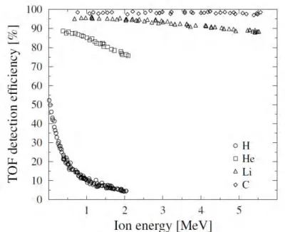
Figure 20: The efficiency of the ToF-ERDA for light elements depends on the ion energy. Usually, ERDA uses ion energies of tens or hundreds MeVs, but measuring light elements by ToF-ERDA requires lowering incident ion energy significantly. [53]
A typical ToF-system uses two ToF timing detectors and a conventional silicon detector. The first timing detector is placed at a fixed scattering angle near the sample. The second timing detector is placed at a variable angle at a longer distance.
Figure 21: A typical ToF-ERDA uses two timing detectors that acquire the timing signal using carbon foils. The resolution depends on the stopping power of the coils and the distance between timing detectors. [52]
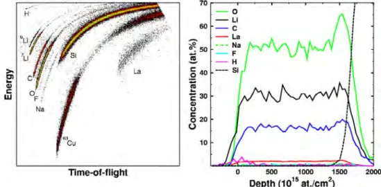
The acquired plot is not a spectrum, but a scatterplot as seen in Figure 22. [54]
Figure 22: The ToF-ERDA produces a scatterplot. There is a visible correlation between atomic mass and in the position on the X-Y axis. The color collaborates to the concentration. The scatterplot is converted to a depth profile using computational methods. [52]
The timing detectors use a carbon foil to pick-up the timing signal and the detection efficiency for light elements is proportional to the stopping force and ion scattering in the carbon foils. The depth resolution is mainly limited by the timing resolution of the timing detectors and kinematic spreading in the sample. [52] ToF-ERDA sensitivity can be∼10 ppm depending on the measurement conditions. The
depth profiling is possible up to several microns. The depth resolution is ∼10 nm
near the surface and decreases when the depth is increased. Unlike with the silicon detectors, the acquired scatterplot is evaluated using computational methods to extract the elemental information. [54]
The magnetic spectrometers use a magnetic field to measure charged recoiled particles that have different trajectory depending on their mass and velocity. All
recoils that have similar trajectory has same charge/momentum ratio and the recoils are identified by the energy in the detection plane. The high energy resolution is obtained by determining the particle location in the detection plane. Therefore, the depth resolution is drastically improved compared to the silicon detectors. [53] This type of detector allows usage of a very low ion dose for accurate measurements and enables a monolayer resolution at the surface. The depth resolution can be increased further using coincident elastic recoil detection (CERD) that requires very thin sample since both scattered and recoiled particles are measured. [50]
The collision cascade is a fundamental requirement for SIMS, whereas for ERDA, multiple scatterings will distort the elemental spectrum. Monte Carlo -simulations can be used to verify the amount of multiple scatterings to obtain reliable data. [52] Analogous to RBS, the sample should be laterally homogeneous and have a smooth surface. The beam size and the incident angle are critical for ERDA since all detected recoils should be ejected at the same direction and pass over the same path for accurate analysis. [50] Unlike in RBS, the scattering cross-section is large since the probability for forward scattering is high and the probability does not change with the mass of the element.
Indeed, ERDA is a unique method to get an accurate depth profile without destroying the sample. When combined to the ToF-detector, the tool is very accu-rate for thin-film analysis, such as atomic layer deposited (ALD) thin-films with a resolution of 0.5 at.%. [53] For the best accuracy, ERDA and RBS should be used as complementary techniques. ERDA is especially popular in polymer sciences since it can study the hydrogen content accurately. It should be remembered that the high energy beam might decompose or sputter the sample that lead to inaccurate impurity analysis.
4.8
Comparison
The reviewed techniques were distinguished into two groups based on the probing species as shown in Table 2. From the reviewed techniques, the two main categories were: a) probing by electrons b) probing by X-rays or ions. However the applications of each tool are discussed in Section 6 and this section focuses on comparative discussion.
XPS is probably the most used surface analysis tool. AES is almost similar to XPS, however, XPS results are easier to interpret. Furthermore, both techniques are limited to the surface area and the maximum sputtering depth is usually in the range of 1µm. In other words, they are most commonly used for surface characterization similar to ERDA and RBS. In contrast, SIMS can be used to characterize films up to 20 µm. However, SIMS requires standards for quantitative results. The standardization can be acquired by other tools such as RBS or ERDA [50]. Currently, there are tools available that combine both AES and XPS. The combination enables more accurate characterization of complex materials since both techniques have different efficiency ranges as seen in Figure 8. However, the surface charging is a major problem for AES. On the other hand, AES has a superior lateral resolution to XPS. Nevertheless, the popularity of the tool is not a guarantee of superiority.