Available online at http://journal.walisongo.ac.id/index.php/jnsmr
Current State: The Development of Thin Film Solar Cells Based on
Kesteritee Compound
Fianti1, Badrul Munir2, Kyoo Ho Kim3, and Mohammad Ikhlasul Amal4
1Department of Physics, Semarang State University, Central Java, Indonesia 2Department of Metallurgical Engineering, University of Indonesia, Indonesia
3Department of Materials Science and Engineering, Yeungnam University, 214-1 Daedong, Gyeongsan,
Gyeongbuk 712-749, Republic of Korea.
4Indonesian Institut of Sciences (LIPI), South Tangerang, Indonesia.
Corresponding author: [email protected] Recived: 17 March 2016, Revised: 30 April 2016 Accepted: 10 June 2016.
Abstracts
Thin film solar cell experience fast development, especially for thin film solar cell CdTe and Cu(In,Ga)Se2(CIGS). However, the usage of rare element in the nature
such as In, Te, and Ga and toxic such as Cd give limitation in the future development and production growth in big scale. Development of other alternative compound with maintain the profit of electronic and optic character which get from CIGS chalcopyrite compound will be explain. Compound of Cu2ZnSnSe4 (CZTSe) is downward compound from CIGS with substitute the In
and Ga element with Zn and Sn. The compound kesterite structure can be modified with variation of chalcogen element to get wanted character in solar cell application. Efficiency record of photovoltaic devices conversion used this compound or downward reach 9.7%.©2016 JNSMR UIN Walisongo. All rights reserved.
Key words: Thin Film; Solar Cell; Kesteritee Coumpond.
1.
Introduction
Solar cell or it can be called photovoltaic, is a devicessystem that converse sun light to become electricity energy. In generally at 2010, installation of solar cell have gain number 18,2 gigawatt (GW) with statistical growth 139% per year from the year before. This development is good if its compared with the global installation scope amounted 52
fulfill in solar cell development: i) high conversion efficiency, ii) long life devices system, iii)material availability, iv) cheap production cost for big scale.
In market scope of solar cell, solar cell based silicon is first generation development of photovoltaic technology, it is dominate in market segment amounted 80%. the dominate of silicon solar cell is because by historical the
development of silicon material in
semiconductor and electronic application is long standing conducted, so that the usage in application of solar cell only become the diversification of silicon material application for silicon industries in proper place. Beside that, availability of silicon as basic material is over abundance and environment impact of silicon degradation is low. Until now, it is note down that efficiency of silicon solar cell is 25% for laboratory scale of submodule crystalline silicon [2] and 23% for silicon of terrestrial module crystalline [3], both is development by UNSW. Solar cell of crystalline silicon need silicon wafer is thick as 250-300 µm for absorb light fraction by efficient. Besides that, crystal formation should be single complete because there is granule limit became active location to recombination center. This both condition caused high production cost of silicon solar cell so it is difficult to compete with other energy power source technology. Diversification of silicon usage for solar cell application such as multi-crystalline silicon, amorphous silicon, thin film silicon also developed but not gain success yet such as crystalline silicon. Deficiencies of solar cell based silicon is become a reason for the development of second solar cell that needed less material and easy process.
Second generation of photovoltaic
technology is solar cell of thin film shows the increasing continue with market segment gain amounted 15% in year 2010 from 6% in year 2005 [1]. the definition of thin film material is more precisely conducted based on production process better than based on thickness border, that is material that manufactured with nucleation process and random growth from molecular/ionic/atomic species that reacted
or condensation with complete on a substrate. In general, method for deposition material of thin film can be divide in two, that is vacuum method (thermal evaporation, sputtering, laser deposition, atomic layer deposition, etc) and non-vacuum (electro-deposition, sol-gel, spray pyrolisis, etc). The atomic process, nucleation, and random growth can be produced new and exotic characteristic of thin film material. This characteristics can controlled and reproduced through variation of deposition parameter.
Material that can be application as absorb layer or active layer on solar cell by ideal should have band gap value ~1.5 eV, high optic
absorption (~105), high quantum efficiency
value, long distance diffusion, low
recombination velocity, and it can formed good electronic junction. Optimum thickness from active layer of solar cell is reverse with optic absorption coefficient, so the material thickness can be reduction as far as the light character as recombination center. Some materials which has character as called above is: CdTe, GaAs, Cu2S, Cu2O, Zn3P2, and compound or descend combination such as chalcopyrite (I-III-VI). silicon material also develop with thin film approach with amorphous or crystalline.
However, at the moment the solar cell of thin film has limit because the technology development is not in proper place yet,
included the intense of infrastructure
involve the technology and material of non-conventional nano-structure such as multi-layer/tandem cell, sensitive color cell (dye-sensitized solar cell), organic cell, intermediate band gap cell, quantum dot, and hot-carriers cell. Because of the unripe development that compared with the two pioneer, the third generation of solar cell is not show the significant penetration. For example, efficiency record for DSSC is 10,4% [4] and solar cell of organic polymer: 5,15% [5]. For tandem cell GaInP/GaAs/Ge gain the efficiency record is 32%, it is the higher among the technology of other solar cell, however the complex technology usage caused the technology can not cut down to big scale. It is also become general problem for third technology of solar cell. Figure 1 is illustrated the estimation of the cost that needed and conversion efficiency that produced for each generation [6]. Solar cell of crystalline silicon is difficult to understanding in gain the low production cost target, while the technology of thin film is believed has potential as alternative in short term time. This article is deeply discuss the development trend, opportunity and challenge of solar cell of thin film especially based on material of kesteritecompound.
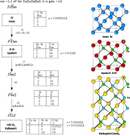
2. Chalcopyrite Compound and The Downward
Development of new material for
semiconductor and electronic application can be done with the downward from the element of group IV with combination of element in related group, such as binary compound with sphalerite and chalcopyrite ternary structure. The compound of the downward multi element have new character that different
with origin element/compound. The
systematic of downward and element
combination so its produced structure and different compound combination such as shown at Figure 2.
Sphalerite compound II-VI CdTe and the Chalcopyrite compound I-III-VI2 CuInS2 (CIS) is material that by history is previous and started development project of electricity generator of solar power based CdTe that biggest in the world with capacity of 2 GW in 2010 with finishing schedule in 2019 [9]. For CIS material, the development is done a modification with substitute a part of indium atom with galliumatom, formed Cu(In,Ga)Se2 (CIGSe) compound. Module of solar cell with active layer used Cu(In,Ga)Se2 material had gain efficiency amounted 19,4% for laboratory scale cell (NREL) [10] and 13,8% for terrestrial module that develop by Miasole [11].
Pigure 1. Analysis of efficiency cost for solar cell of crystalline silicon, thin film, and third generation (adapted from ref [6]).
character . Such as substitute the entire or partial of selenium with sulfur can change the level of conductivity ribbon and valence so make possible to variate the band gap value from ~1.1 eV for Cu(In,Ga)Se2, it is gain ~1.5
eV for Cu(In,Ga)S2 (CIGS). The freedom in developing the wanted character in compound based chalcopyrite made it as research focus in many laboratory.
Figure 2. Downward systematic of element in group IV become ternary downward compound I-III-VI2 along
with the crystal parameter of each compound.
However, regardless from potential that shown by material of CdTe and CIGS, both those technology contains rare element that found on earth that is indium, gallium, and tellurium. Beside that cadmium is known as element which have high toxic. The problem of
Cu2ZnSnSe4 (CZTSe),is downward compound from CIGS which gain by substitute the indium and gallium element with zinc and tin that more cheaper and environment friendly.
Even though, it is adopted the same crystal element, that is chalcopyrite, but because of the changing of atom position which substituted, so quartener compound have own crystal structure that is kesteriteor stannite, where is the different is in the organization of element atom I in crystal sub -kisi. The analysis result used neutron diffraction [12] had confirm that CZTSe have kesterite structure that stannite structure which supported by theoretic calculation [13]. In the same with CIGS, this compound can modified with changing kalkogen element to get different material characteristic, so it can be made three variation compound that is CZTSe, CZTS, or partial substitute produced CZTSSe.
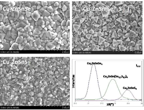
This material fabrication can be done with various method such as explain before. One of
the method that wide application is
combination of vacuum deposition with selenization/sulfurization thermal reaction. Superiority of the method is stability and reproducible and easy to develop in big scale. Our laboratory develop deposition method with two steps that is production of metal precursorswith sputtering target alloy
Cu-Sn-Zn and selenization/sulfurization on
temperature 400 C or higher to produce single phase of CZTSSe. Picture 3 shows that micro structure of three compound that is CZTSe, CZTS, and CZTSSe which produced used this method. It is seen difference contents of S/Se element, it give impact on micro-structure visualization where is CZTSe has bigger granule than CZTS. Beside that diffraction pattern of X-ray for 112 area shows
the difference of intensity and position θ as
deviation by stoichiometry and produce
secondary phase that is unwanted [14].
CZTSe had been researched have
character which can be application for solar cell, Wibowo et.al, report that film of CZTSe with high absorption coefficient amounted 104 cm-1, resistance amounted .4 Ωcm and carrier concentration amounted 1019 cm-3[15]. In the first development of photovoltaic devices used this material in 1996, its reported the efficiency value amounted 0.66% for devices of solar cell glass structured /Mo/CZTS/CdS/ZnO:Al [16].The number is increase become 2,3% in the next year based on the development that conducted by Friedlmeier et al. [17]. For this time, the efficiency record is 6.8% for solar cell of CZTS [18], 3.2% for solar cell of CZTSe [19], and 9.7%% for solar cell of CZTSSe [20]. For the both devices mention before used technology of vacuum deposition while for solar cell of CZTSSe used process of chemical synthesis based solution. Beside that, presentation above also describe the development of solar
cell used CZT(Se,S) material is slow
development with increasing of efficiency record more than one decade, but for this time the development shows good potential so projection of market penetration is conducted more faster. Table 2 shows the devices development of solar cell used CZT(Se,S) material with different fabrication method.
3.
Devices of Solar Cell CZTSSe
circuit voltage, Jsc = short-circuit current density, FF = fill factor).
Evaluation from the result of devices characteristic found several thing that become deficiency and cause of the performed limited that is: first, good thin film of solar cell have
contradiction between Voc and Eg/q
appropriate to 0.5 V, where is Eg is band gap and q is electron capacity. While, this devices have Eg/q value more than 0.6 V. it is give
indication of main recommendation
mechanism which dominated by interface recommendation. Second, FF value is lower its might be caused by the higher of obstruction as consequence of obstacle of back contact in interface area between Mo and CZTSSe so its push down the transportation of majority carrier (hole). Third, response of quantum efficiency for big wave long area of band gap limit is low, with short minority carrier life time more over ~1.2 ns.
Table 2. Summary of devices efficiency of solar cell CZT(Se,S) with different fabrication method
Year Material Fabrication method Efficiency (%) Ref.
1997 CZTS Evaporation Electron beam + sulfurization 0.66 [16]
1997 CZTSe Evaporation multi-element 0.6 [17]
1997 CZTS Evaporation multi-element 2.3 [17]
2001 CZTS Evaporation multi-element 2.62 [21]
2003 CZTS Evaporasi element + ZnS + control doping Na 5.45 [22]
2007 CZTS RF co-sputtering Cu-ZnS-SnS 5.74 [23]
2008 CZTS RF co-sputtering Cu-ZnS-SnS + annealing + etching 6.77 [18]
2008 CZTS Deposition pulsed-laser 0.64 [24]
2008 CZTS Elektrodeposition Zn-Sn-Cu + sulfurization 0.8 [25]
2009 CZTSe Sputtering multi layers + selenization 3.2 [26]
2009 CZTS Evaporation Cu-Sn-S-ZnS 1.1 [27]
2009 CZTS Elektrodeposition element + sulfurization 0.98 [28]
2009 CZTS Co-elektrodeposition 3.16 [29]
2009 CZTS Co-elektrodeposition + etching + annealing 3.4 [30]
2009 CZTS Sol-gel + spin coating 1.01 [31]
2009 CZTS Sol-gel + spin coating 1.61 [32]
2009 CZTS Deposition nanoparticle 0.23 [33]
2009 CZTS Deposition nanoparticle + annealing 0.74 [34]
2009 CZTSe Single grain layer 2.16 [35]
2010 CZTS Evaporation Cu-Sn-S-ZnS + etching 4.1 [36]
2010 CZTS Evaporation Cu-Zn-Sn-S + annealing 6.8 [37]
2010 CZTS Elektrodeposition Zn-Cu-Sn-Cu + sulfurization +
etching
3.2 [38]
2010 CZTS Ball-milling + screen printing + hot pressing 0.49 [39]
2011 CZTSSe Chemical reaction with hydrazine solvent 9.7 [20]
Figure 4. The curve of J-V light under simulation of AM 1.5 light for devices solar cell of soda lime/Mo/CZTSSe/CdS/ZnO/ITO (insert) with efficiency amounted 9.7%, Voc=0.448 V, Jsc=32.3 mA/cm2, and FF=67% [20].
4.
Conclusion
and
Future
Development
material synthesis is easiest of element evaporation such as Sn and Zn and formation of seconder phase that can limit the solar cell perform.
The other thing that should be done is doing research of phase change in formation of CZT(S,Se) compound, it is needed detail understanding of interface character, optimum layer in devices interface, knowledge of natural defects character in active layer, and test of long life stability towards devices of solar cell CZT(S,Se). The beginning result that explanation before is show the future chances of solar cell CZT(S,Se). It is expected that the intense research and development in the future can realization the cheap and save solar cell for environment.
Acknowledgment
The author wish to thank to Department
of Physics, Semarang State University,
Department of Metallurgical Engineering, University of Indonesia, Department of Materials Science and Engineering, Yeungnam University, Indonesian Institut of Sciences (LIPI), South Tangerang, Indonesia for support in this research.
References
[1] Solarbuzz Reports World Solar Photo-voltaic Market Grew to 18.2 Gigawatts in
2010, Up 139% Y/Y,
http://www.prweb.com, 2011.
[2] J. Zhao, A. Wang, M.A. Green, F. Ferrazza.
Novel . % efficient honeycomb te
x-tured multicrystalline and 24.4%
monocrystalline silicon solar cells. Ap-plied Physics Letters 73, 1998, pp.1991– 1993.
[3] J.Zhao, A. Wang, F. Yun, G.Zhang, D.M. Roche, S.R. Wenham, M.A. Green. 20,000
PERL silicon cells for the 6 World Solar Challenge solar car race. Progress in Photovoltaics: Research and Applica-tions. 5, pp. 269–276, 1997.
[4] M. Morooka, K. Noda. Development of dye-sensitized solar cells and next
gen-eration energy devicess, 88th Spring Meeting of The Chemical Society of Japan, Tokyo, 26 March 2008.
[5] http://www.konarka.com (2011)
[6] M.A. Green, J. Zhao, A. Wang and S.R. Wenhan, Progress and outlook for high efficiency crystalline silicon solar cells, Solar Energy Materials and Solar Cells 65, pp. 9–16, 2001.
[7] X. Wu, J.C. Keane, R.G. Dhere, C. DeHart, A. Duda, T.A. Gessert, S. Asher, D.H. Levi, P. Sheldon, 16.5%- efficient CdS/CdTe polycrystalline thin-film solar cell, Pro-ceedings of 17th European Photovoltaic Solar Energy Conference, Munich, 22–26, pp. 995–1000, October 2001.
[8] D. Cunningham, K. Davies, L. Grammond,
E. Mopas, N. O Connor, M. Rubcich, M. Sadeghi, D. Skinner, T. Trumbly. Large area ApolloTM module performance and reliability, Conference Record, 28th IEEE Photovoltaic Specialists Conference, Alas-ka, September, pp.13–18, 2000.
[9] I. Repins, M. Contreras,Y. Romero, Y. Yan, W. Metzger, J.Li, S. Johnston, B. Egaas, C. DeHart, J. Scharf, B.E McCandless, R.
Noufi. Characterization of
19.9%-efficienct CIGS absorbers, 33th IEEE Photovoltaics Specialists Conference Rec-ord, 2008.
[10] http://www.miasole.com, 2011.
[11] S. Chorr, The crystal structure of kesteritee type compounds: A neutron and X-ray diffraction study, Solar Energy Materials & Solar Cells, 95, pp.1482-1488, 2011.
[12] T. Maeda, S. Nakamura, T. Wada, Phase stability and electronic strucutre of
In-free photovoltaic semiconductors,
Cu2ZnSnSe4 and Cu2ZnSnS4 by first principles calculation, Mater. Res. Soc. Symp. Proc. 1165, pp. M04-03, 2009. [13] I. Amal, K. Kyoo Ho, Formation of CZTSeS
by two step fabrication, in submission, 2011.
chalcogenide targets, Journal of Physics and Chemistry of Solids 68, pp.1908-1913, 2007.
[15] H. Katagiri, N. Sasaguchi, S. Hando, S. Hoshino, J. Ohashi and T. Yokota, Prepa-ration and evaluation of Cu2ZnSnS4 thin films by sulfurization of E-B evaporated precursors, Sol. Energy Mater. Sol. Cells 49, pp. 407–414, 1997.
[16] Th.M. Friedlmeier, N. Wieser, Th. Walter,
H. Dittrich, H.-W. Schock,
Heterojunctions based on Cu2ZnSnS4 and Cu2ZnSnSe4 thin films, in:
Proceed-ings of the 14th European Photovoltaic Solar Energy Conference, pp. 1242–1245, 1997.
[17] H. Katagiri, K. Jimbo, S. Yamada, T. Kamimura, W.S. Maw, T. Fukano, T. Ito and T. Motohiro, Enhanced conversion efficiencies of Cu2ZnSnS4-based thin film solar cells by using preferential selenisation of magnetron sputtered precursors, Prog. Photovolt.: Res. Appl. 17, pp. 315–319, 2009.
[19] D.B. Mitzi, O. Gunawan, T. K. Todorov, K. Wang, S. Guha, The path towards a
high-performance solution-processed
kesteritee solar cell, Sol. Energy Mater. Sol. Cells. 95, pp. 1421–1436, 2011. [20] H. Katagiri, K. Saitoh, T. Washio, H.
Shi-nohara, T. Kurumadani and S. Miyajima, Development of thin film solar cell based on Cu2ZnSnS4 thin films, Sol. Energy Ma-ter. Sol. Cells 65, pp. 141–148, 2001. [21] H. Katagiri, K. Jimbo, K. Monya, K.
Tsuchida, Solar cell without environ-mental pollution by using CZTS thin film, in: Proceedings of the World Conference on Photvoltaics Energy Conversion III, pp. 2874–2879, 2003.
[22] K. Jimbo, R. Kimura, T. Kamimura, S. Yamada, W.S. Maw, H. Araki, K. Oishi and H. Katagiri, Cu2ZnSnS4-type thin film
so-lar cells using abundant materials, Thin Solid Films 515, pp. 5997–5999, 2007. [23] K. Moriya, K. Tanaka and H. Uchiki,
Cu2ZnSnS4 thin films annealed in H2S atmosphere for solar cell absorber pre-pared by pulsed laser deposition, Jpn. J. Appl. Phys. 47, pp. 602–604, 2008.
[24] J.J. Scragg, P.J. Dale, L.M. Peter, G. Zoppi and I. Forbes, New routes to sustainable photovoltaics: evaluation of Cu2ZnSnS4 as an alternative absorber material, Phys. Status Solidi B 245, pp. 1772–1778, 2008.
[25] G. Zoppi, I. Forbes, R.W. Miles, P.J. Dale, J.J. Scragg and L.M. Peter, Cu2ZnSnSe4 thin film solar cells produced by selenisation of magnetron sputtered precursors, Prog. Photovolt.: Res. Appl. 17, pp. 315–319, 2009.
[26] A. Weber, H. Krauth, S. Perlt, B. Schubert, I. Kötschau, S. Schorr and H.W. Schock, Multi-stage evaporation of Cu2ZnSnS4 thin films, Thin Solid Films 517, pp. 2524–2526, 2009.
[27] H. Araki, Y. Kubo, A. Mikaduki, K. Jimbo, W.S. Maw, H. Katagiri, M. Yamazaki, K. Oishi and A. Takeuchi, Preparation of Cu2ZnSnS4 thin films by sulfurizing elec-troplated precursors, Sol. Energy Mater. Sol. Cells 93, pp. 996–999, 2009.
[28] H. Araki, Y. Kubo, K. Jimbo, W.S. Maw, H. Katagiri, M. Yamazaki, K. Oishi and A. Takeuchi, Preparation of Cu2ZnSnS4 thin films by sulfurization of co-precursors: novel low-cost perspective, Thin Solid Films 517, pp. 2511–2514, 2009.
Energy Mater. Sol. Cells 93, pp. 583–587, 2009.
[31] N. Moritake, Y. Fukui, M. Oonuki, K. Tanaka and H. Uchiki, Preparation of Cu2ZnSnS4 thin film solar cells under non-vacuum condition, Phys. Status Soli-di C 6, pp. 1233–1236, 2009.
[32] C. Steinhagen, M.G. Panthani, V. Akhavan, B. Goodfellow, B. Koo and B.A. Korgel, Synthesis of Cu2ZnSnS4 nanocrystals for use in low-cost photovoltaics, J. Am. Chem. Soc. 131, pp. 12554–12555, 2009. [33] Q. Guo, H.W. Hillhouse and R. Agrawal,
Synthesis of Cu2ZnSnS4 nanocrystal ink and its use for solar cells, J. Am. Chem. Soc. 131, pp. 11672–11673, 2009.
[34] K. Timmo, M. Altosaar, J. Raudoja, K. Muska, M. Pilvet, M. Kauk, T. Varema, M. Danilson, O. Volobujeva and E. Mellikov,
Sulfur-containing Cu2ZnSnSe4
monograin powders for solar cells, Sol. Energy Mater. Sol. Cells. 94, pp. 1889– 1892, 2010.
[35] B.-A. Schubert, B. Marsen, S. Cinque, T. Unold, R. Klenk, S. Schorr, H.-W. Schock, Cu2ZnSnS4 thin film solar cells by fast coevaporation, Prog. Photovolt.: Res. Appl. 2010.
[36] K. Wang, O. Gunawan, T. Todorov, B. Shin, S.J. Chey, N.A. Bojarczuk, D. Mitzi and S. Guha, Thermally evaporated Cu2ZnSnS4 solar cells, Appl. Phys. Lett. 97, pp. 143508 (3 pp), 2010.
[37] J.J. Scragg, D.M. Berg and P.J. Dale, A 3.2% efficient kesteritee devices from electrodeposited stacked elemental lay-ers, J. Electroanal. Chem. 646, pp. 52–59, 2010.
![Figure 4. The curve of J-V light under simulation of AM 1.5 light for devices solar cell of soda lime/Mo/CZTSSe/CdS/ZnO/ITO (insert) with efficiency amounted 9.7%, Voc=0.448 V, Jsc=32.3 mA/cm2, and FF=67% [20]](https://thumb-ap.123doks.com/thumbv2/123dok/1895394.1586446/7.612.72.548.102.461/figure-simulation-light-devices-cztsse-insert-efficiency-amounted.webp)
