General Description
The MAX220–MAX249 family of line drivers/receivers is intended for all EIA/TIA-232E and V.28/V.24 communica-tions interfaces, particularly applicacommunica-tions where ±12V is not available.These parts are especially useful in battery-powered sys-tems, since their low-power shutdown mode reduces power dissipation to less than 5µW. The MAX225, MAX233, MAX235, and MAX245/MAX246/MAX247 use no external components and are recommended for appli-cations where printed circuit board space is critical.
________________________Applications
Portable Computers
Low-Power Modems
Interface Translation
Battery-Powered RS-232 Systems
Multidrop RS-232 Networks
Next-Generation Device Features
♦
♦
For Low-Voltage, Integrated ESD Applications
MAX3222E/MAX3232E/MAX3237E/MAX3241E/
MAX3246E: +3.0V to +5.5V, Low-Power, Up to
1Mbps, True RS-232 Transceivers Using Four
0.1µF External Capacitors (MAX3246E Available
in a UCSP™ Package)
♦
♦
For Low-Cost Applications
MAX221E: ±15kV ESD-Protected, +5V, 1µA,
Single RS-232 Transceiver with AutoShutdown™
MAX220–MAX249
Drivers/Receivers
________________________________________________________________Maxim Integrated Products 1
Selection Table
PART MAX220CPE+ MAX220CSE+
MAX220CWE+ 0°C to +70°C
0°C to +70°C 0°C to +70°C
TEMP RANGE PIN-PACKAGE
16 Plastic DIP 16 Narrow SO 16 Wide SO
MAX220C/D 0°C to +70°C Dice*
MAX220EPE+ MAX220ESE+
MAX220EWE+ -40°C to +85°C
-40°C to +85°C
-40°C to +85°C 16 Plastic DIP 16 Narrow SO 16 Wide SO
MAX220EJE -40°C to +85°C 16 CERDIP
MAX220MJE -55°C to +125°C 16 CERDIP
Power No. of Nominal SHDN Rx
Part Supply RS-232 No. of Cap. Value & Three- Active in Data Rate
Number (V) Drivers/Rx Ext. Caps (µF) State SHDN (kbps) Features
MAX220 +5 2/2 4 0.047/0.33 No — 120 Ultra-low-power, industry-standard pinout
MAX222 +5 2/2 4 0.1 Yes — 200 Low-power shutdown
MAX223 (MAX213) +5 4/5 4 1.0 (0.1) Yes ✔ 120 MAX241 and receivers active in shutdown
MAX225 +5 5/5 0 — Yes ✔ 120 Available in SO
MAX230 (MAX200) +5 5/0 4 1.0 (0.1) Yes — 120 5 drivers with shutdown
MAX231 (MAX201) +5 and 2/2 2 1.0 (0.1) No — 120 Standard +5/+12V or battery supplies;
+7.5 to +13.2 same functions as MAX232
MAX232 (MAX202) +5 2/2 4 1.0 (0.1) No — 120 (64) Industry standard
MAX232A +5 2/2 4 0.1 No — 200 Higher slew rate, small caps
MAX233 (MAX203) +5 2/2 0 — No — 120 No external caps
MAX233A +5 2/2 0 — No — 200 No external caps, high slew rate
MAX234 (MAX204) +5 4/0 4 1.0 (0.1) No — 120 Replaces 1488
MAX235 (MAX205) +5 5/5 0 — Yes — 120 No external caps
MAX236 (MAX206) +5 4/3 4 1.0 (0.1) Yes — 120 Shutdown, three state
MAX237 (MAX207) +5 5/3 4 1.0 (0.1) No — 120 Complements IBM PC serial port MAX238 (MAX208) +5 4/4 4 1.0 (0.1) No — 120 Replaces 1488 and 1489
MAX239 (MAX209) +5 and 3/5 2 1.0 (0.1) No — 120 Standard +5/+12V or battery supplies; +7.5 to +13.2 single-package solution for IBM PC serial port
MAX240 +5 5/5 4 1.0 Yes — 120 DIP or flatpack package
MAX241 (MAX211) +5 4/5 4 1.0 (0.1) Yes — 120 Complete IBM PC serial port
MAX242 +5 2/2 4 0.1 Yes ✔ 200 Separate shutdown and enable
MAX243 +5 2/2 4 0.1 No — 200 Open-line detection simplifies cabling
MAX244 +5 8/10 4 1.0 No — 120 High slew rate
MAX245 +5 8/10 0 — Yes ✔ 120 High slew rate, int. caps, two shutdown modes MAX246 +5 8/10 0 — Yes ✔ 120 High slew rate, int. caps, three shutdown modes MAX247 +5 8/9 0 — Yes ✔ 120 High slew rate, int. caps, nine operating modes MAX248 +5 8/8 4 1.0 Yes ✔ 120 High slew rate, selective half-chip enables MAX249 +5 6/10 4 1.0 Yes ✔ 120 Available in quad flatpack package
For pricing, delivery, and ordering information, please contact Maxim Direct at 1-888-629-4642,
Ordering Information
+Denotes a lead(Pb)-free/RoHS-compliant package. *Contact factory for dice specifications.
Ordering Information continued at end of data sheet.
MAX220–MAX249
ABSOLUTE MAXIMUM RATINGS—MAX220/222/232A/233A/242/243
ELECTRICAL CHARACTERISTICS—MAX220/222/232A/233A/242/243
(VCC= +5V ±10%, C1–C4 = 0.1µF‚ MAX220, C1 = 0.047µF, C2–C4 = 0.33µF, TA= TMINto TMAX‚ unless otherwise noted.) (Note 3)
Note 1:For the MAX220, V+ and V- can have a maximum magnitude of 7V, but their absolute difference cannot exceed 13V.
Note 2:Input voltage measured with TOUT in high-impedance state, VSHDNor VCC= 0V.
Stresses beyond those listed under “Absolute Maximum Ratings” may cause permanent damage to the device. These are stress ratings only, and functional operation of the device at these or any other conditions beyond those indicated in the operational sections of the specifications is not implied. Exposure to absolute maximum rating conditions for extended periods may affect device reliability.
(Voltages referenced to GND.)
VCC...-0.3V to +6V V+ (Note 1) ...(VCC- 0.3V) to +14V V- (Note 1) ...+0.3V to -14V Input Voltages
TIN ...-0.3V to (VCC- 0.3V) RIN (Except MAX220) ...±30V RIN (MAX220) ...±25V TOUT (Except MAX220) (Note 2) ...±15V TOUT (MAX220)...±13.2V Output Voltages
TOUT...±15V ROUT...-0.3V to (VCC+ 0.3V) Driver/Receiver Output Short Circuited to GND...Continuous Continuous Power Dissipation (TA= +70°C)
16-Pin Plastic DIP (derate 10.53mW/°C above +70°C)..842mW 18-Pin Plastic DIP (derate 11.11mW/°C above +70°C)..889mW 20-Pin Plastic DIP (derate 8.00mW/°C above +70°C) ..440mW
16-Pin Narrow SO (derate 8.70mW/°C above +70°C) ...696mW 16-Pin Wide SO (derate 9.52mW/°C above +70°C)...762mW 18-Pin Wide SO (derate 9.52mW/°C above +70°C)...762mW 20-Pin Wide SO (derate 10.00mW/°C above +70°C)....800mW 20-Pin SSOP (derate 8.00mW/°C above +70°C) ...640mW 16-Pin CERDIP (derate 10.00mW/°C above +70°C)...800mW 18-Pin CERDIP (derate 10.53mW/°C above +70°C)...842mW Operating Temperature Ranges
MAX2_ _AC_ _, MAX2_ _C_ _ ...0°C to +70°C MAX2_ _AE_ _, MAX2_ _E_ _ ...-40°C to +85°C MAX2_ _AM_ _, MAX2_ _M_ _ ...-55°C to +125°C Storage Temperature Range ...-65°C to +160°C Lead Temperature (soldering, 10s) ...+300°C Soldering Temperature (reflow)
20 PDIP (P20M+1) ...+225°C All other lead(Pb)-free packages...+260°C All other packages containing lead(Pb) ...+240°C
PARAMETER CONDITIONS MIN TYP MAX UNITS
RS-232 TRANSMITTERS
Output Voltage Swing All transmitter outputs loaded with 3k to GND ±5 ±8 V
Input Logic-Low Voltage 1.4 0.8 V
All devices except MAX220 2 1.4
Input Logic-High Voltage
MAX220: VCC = +5.0V 2.4
V
All except MAX220, normal operation 5 40
Logic Pullup/lnput Current VSHDN = 0V, MAX222/MAX242, shutdown,
MAX220 ±0.01 ±1
μA
VCC = +5.5V, VSHDN = 0V, VOUT = ±15V,
MAX222/MAX242 ±0.01 ±10
VOUT = ±15V ±0.01 ±10
Output Leakage Current
VCC = VSHDN = 0V
MAX220, VOUT = ±12V ±25
μA
Data Rate 200 116 kbps
Transmitter Output Resistance VCC = V+ = V- = 0V, VOUT = ±2V 300 10M
VOUT = 0V ±7 ±22
Output Short-Circuit Current VOUT = 0V
MAX220 ±60 mA
RS-232 RECEIVERS
±30
RS-232 Input Voltage Operating Range
MAX220 ±25 V
All except MAX243 R2IN 0.8 1.3
RS-232 Input Threshold Low VCC = +5V
MAX243 R2IN (Note 4) -3 V
All except MAX243 R2IN 1.8 2.4
RS-232 Input Threshold High VCC = +5V
MAX220–MAX249
ELECTRICAL CHARACTERISTICS—MAX220/222/232A/233A/242/243 (continued)
(VCC= +5V ±10%, C1–C4 = 0.1µF‚ MAX220, C1 = 0.047µF, C2–C4 = 0.33µF, TA= TMINto TMAX‚ unless otherwise noted.) (Note 3)
PARAMETER CONDITIONS MIN TYP MAX UNITS
All except MAX220/MAX243, VCC = +5V, no
hysteresis in shutdown 0.2 0.5 1.0
MAX220 0.3
RS-232 Input Hysteresis
MAX243 1
V
3 5 7
RS-232 Input Resistance TA = +25°C (MAX220)
3 5 7 k
IOUT = 3.2mA 0.2 0.4
TTL/CMOS Output Voltage Low
IOUT = 1.6mA (MAX220) 0.4
V
TTL/CMOS Output Voltage High IOUT = -1.0mA 3.5 VCC - 0.2 V
Sourcing VOUT = VGND -2 -10
TTL/CMOS Output Short-Circuit Current
Sinking VOUT = VCC 10 30
mA
TTL/CMOS Output Leakage Current VSHDN = VCC or VEN = VCC (VSHDN = 0V for
MAX222), 0V VOUT VCC ±0.05 ±10 μA
EN Input Threshold Low MAX242 1.4 0.8 V
EN Input Threshold High MAX242 2.0 1.4 V
Supply Voltage Range 4.5 5.5 V
MAX220 0.5 2
No load MAX222/MAX232A/MAX233A/
MAX242/MAX243 4 10
MAX220 12
VCC Supply Current (VSHDN = VCC),
Figures 5, 6, 11, 19
3k load
both inputs MAX222/MAX232A/MAX233A/
MAX242/MAX243 15
mA
TA = +25°C 0.1 10
TA = 0°C to +70°C 2 50
TA = -40°C to +85°C 2 50
Shutdown Supply Current MAX222/
MAX242
TA = -55°C to +125°C 35 100
μA
SHDN Input Leakage Current MAX222/MAX242 ±1 μA
SHDN Threshold Low MAX222/MAX242 1.4 0.8 V
SHDN Threshold High MAX222/MAX242 2.0 1.4 V
MAX222/MAX232A/
MAX233/MAX242/MAX243 6 12 30
Transition Slew Rate
CL = 50pF to 2500pF,
RL = 3k to 7k,
VCC = +5V, TA =
+25°C, measured from +3V to -3V or -3V to +3V
MAX220 1.5 3 30.0
V/μs
MAX222/MAX232A/
MAX233/MAX242/MAX243 1.3 3.5
tPHLT, Figure 1
MAX220 4 10
MAX222/MAX232A/
MAX233/MAX242/MAX243 1.5 3.5
Transmitter Propagation Delay TLL to RS-232 (Normal Operation)
tPLHT, Figure 1
MAX220 5 10
MAX220–MAX249
__________________________________________Typical Operating Characteristics
MAX220/MAX222/MAX232A/MAX233A/MAX242/MAX243
10
8
-10
0 5 15 25
OUTPUT VOLTAGE vs. LOAD CURRENT
-4
-6
-8 -2 6
4
2
MAX220-01
LOAD CURRENT (mA)
OUTPUT VOLTAGE (V)
10 0
20 0.1µF EITHER V+ OR V- LOADED
VCC = +5V NO LOAD ON TRANSMITTER OUTPUTS (EXCEPT MAX220, MAX233A)
V- LOADED, NO LOAD ON V+
V+ LOADED, NO LOAD ON V-1µF
1µF 0.1µF
11
10
4
0 10 40 60
AVAILABLE OUTPUT CURRENT vs. DATA RATE
6
5 7 9
8
MAX220-02
DATA RATE (kb/s)
OUTPUT CURRENT (mA)
20 30 50
OUTPUT LOAD CURRENT FLOWS FROM V+ TO
V-VCC = +5.25V ALL CAPS
1µF
ALL CAPS 0.1µF
VCC = +4.75V
+10V
-10V
MAX222/MAX242 ON-TIME EXITING SHUTDOWN
+5V +5V
0V 0V
MAX220-03
500µs/div
V+, V- VOLTAGE (V)
1µF CAPS V+ V+
V-SHDN 0.1µF CAPS
1µF CAPS
0.1µF CAPS
ELECTRICAL CHARACTERISTICS—MAX220/222/232A/233A/242/243 (continued)
(VCC= +5V ±10%, C1–C4 = 0.1µF‚ MAX220, C1 = 0.047µF, C2–C4 = 0.33µF, TA= TMINto TMAX‚ unless otherwise noted.) (Note 3)
PARAMETER CONDITIONS MIN TYP MAX UNITS
MAX222/MAX232A/MAX233/
MAX242/MAX243 0.5 1
tPHLR, Figure 2
MAX220 0.6 3
MAX222/MAX232A/MAX233/
MAX242/MAX243 0.6 1
Receiver Propagation Delay RS-232 to TLL (Normal Operation)
tPLHR, Figure 2
MAX220 0.8 3
μs
tPHLS, Figure 2 MAX242 0.5 10
Receiver Propagation Delay RS-232 to
TLL (Shutdown) tPHLS, Figure 2 MAX242 2.5 10
μs
Receiver-Output Enable Time tER MAX242, Figure 3 125 500 ns
Receiver-Output Disable Time tDR MAX242, Figure 3 160 500 ns
Transmitter-Output Enable Time
(SHDN Goes High) tET
MAX222/MAX242, 0.1μF caps (includes charge-pump start-up), Figure 4
250 μs
Transmitter-Output Disable Time
(SHDN Goes Low) tDT
MAX222/MAX242,
0.1μF caps, Figure 4 600 ns
MAX222/MAX232A/MAX233/
MAX242/MAX243 300
Transmitter + to - Propagation Delay
Difference (Normal Operation) tPHLT - tPLHT
MAX220 2000
ns
MAX222/MAX232A/MAX233/
MAX242/MAX243 100
Receiver + to - Propagation Delay
Difference (Normal Operation) tPHLR - tPLHR
MAX220 225
ns
Note 3:All units are production tested at hot. Specifications over temperature are guaranteed by design.
MAX220–MAX249
(Voltages referenced to GND.)
VCC...-0.3V to +6V V+ ...(VCC- 0.3V) to +14V V- ...+0.3V to -14V Input Voltages
TIN ...-0.3V to (VCC+ 0.3V) RIN ...±30V Output Voltages
TOUT ...(V+ + 0.3V) to (V- - 0.3V) ROUT...-0.3V to (VCC+ 0.3V) Short-Circuit Duration, TOUT to GND ...Continuous Continuous Power Dissipation (TA= +70°C)
14-Pin Plastic DIP (derate 10.00mW/°C above +70°C)....800mW 16-Pin Plastic DIP (derate 10.53mW/°C above +70°C)....842mW 20-Pin Plastic DIP (derate 11.11mW/°C above +70°C)....889mW 24-Pin Narrow Plastic DIP
(derate 13.33mW/°C above +70°C) ...1.07W 24-Pin Plastic DIP (derate 9.09mW/°C above +70°C)...500mW 16-Pin Wide SO (derate 9.52mW/°C above +70°C)...762mW 20-Pin Wide SO (derate 10.00mW/°C above +70°C)...800mW 24-Pin Wide SO (derate 11.76mW/°C above +70°C)...941mW
28-Pin Wide SO (derate 12.50mW/°C above +70°C) ...1W 44-Pin Plastic FP (derate 11.11mW/°C above +70°C) ...889mW 14-Pin CERDIP (derate 9.09mW/°C above +70°C) ...727mW 16-Pin CERDIP (derate 10.00mW/°C above +70°C) ...800mW 20-Pin CERDIP (derate 11.11mW/°C above +70°C) ...889mW 24-Pin Narrow CERDIP
(derate 12.50mW/°C above +70°C) ...1W 24-Pin Sidebraze (derate 20.0mW/°C above +70°C)...1.6W 28-Pin SSOP (derate 9.52mW/°C above +70°C)...762mW Operating Temperature Ranges
MAX2 _ _ C _ _...0°C to +70°C MAX2 _ _ E _ _ ...-40°C to +85°C MAX2 _ _ M _ _...-55°C to +125°C Storage Temperature Range ...-65°C to +160°C Lead Temperature (soldering, 10s) ...+300°C Soldering Temperature (reflow)
20 PDIP (P20M+1) ...+225°C 24 PDIP (P24M-1) ...+225°C All other lead(Pb)-free packages...+260°C All other packages containing lead(Pb) ...+240°C
ABSOLUTE MAXIMUM RATINGS—MAX223/MAX230–MAX241
ELECTRICAL CHARACTERISTICS—MAX223/MAX230–MAX241
(MAX223/230/232/234/236/237/238/240/241, VCC = +5V ±10%; MAX233/MAX235, VCC = +5V ±5%‚ C1–C4 = 1.0µF; MAX231/MAX239, VCC= +5V ±10%; V+ = +7.5V to +13.2V; TA= TMINto TMAX; unless otherwise noted.) (Note 5)
Stresses beyond those listed under “Absolute Maximum Ratings” may cause permanent damage to the device. These are stress ratings only, and functional operation of the device at these or any other conditions beyond those indicated in the operational sections of the specifications is not implied. Exposure to absolute maximum rating conditions for extended periods may affect device reliability.
CONDITIONS MIN TYP MAX UNITS
Output Voltage Swing All transmitter outputs loaded with 3kΩto ground ±5.0 ±7.3 V
VCCSupply Current No load,T A= +25°C
5 10
mA
7 15
0.4 1
V+ Supply Current 1.8 5 mA
5 15
Shutdown Supply Current TA= +25°C
15 50
V Input Logic-High Voltage
TIN 2.0
EN, SHDN(MAX223);
EN, SHDN (MAX230/235/236/240/241) 2.4
Logic Pullup Current VTIN = 0V 1.5 200
Receiver Input Voltage
Operating Range -30 +30 V
µA µA
1 10
V
Input Logic-Low Voltage TIN, EN, SHDN(MAX233); EN, SHDN (MAX230/235–241) 0.8
MAX231/239
MAX223/230/234–238/240/241 MAX232/233
PARAMETER
MAX239
MAX230/235/236/240/241 MAX231
mA
MAX220–MAX249
V
0.8 1.2
PARAMETER CONDITIONS MIN TYP MAX UNITS
Normal operation VSHDN= 5V (MAX223)
VSHDN= 0V (MAX235/236/240/241)
1.7 2.4
RS-232 Input Logic-Low Voltage TA= +25°C, VCC= +5V
0.6 1.5
V RS-232 Input Logic-High Voltage TA= +25°C,
VCC= +5V Shutdown (MAX223)
VSHDN= 0V,
VEN= +5V (R4IN‚ R5IN)
1.5 2.4
ELECTRICAL CHARACTERISTICS—MAX223/MAX230–MAX241 (continued)
(MAX223/230/232/234/236/237/238/240/241, VCC = +5V ±10%; MAX233/MAX235, VCC = +5V ±5%‚ C1–C4 = 1.0µF; MAX231/MAX239, VCC= +5V ±10%; V+ = +7.5V to +13.2V; TA= TMINto TMAX; unless otherwise noted.) (Note 5)
Shutdown (MAX223) VSHDN= 0V,
VEN= +5V (R4IN, R5IN) Normal operation
VSHDN= +5V (MAX223)
VSHDN= 0V (MAX235/236/240/241)
RS-232 Input Hysteresis VCC= +5V, no hysteresis in shutdown 0.2 0.5 1.0 V
RS-232 Input Resistance TA= +25°C, VCC= +5V 3 5 7 kΩ
TTL/CMOS Output Voltage Low IOUT= 1.6mA (MAX231/232/233, IOUT= 3.2mA) 0.4 V
TTL/CMOS Output Voltage High IOUT = -1mA 3.5 VCC- 0.4 V
TTL/CMOS Output Leakage Current 0V ≤ROUT≤VCC; VEN= 0V (MAX223);
VEN= VCC(MAX235–241) ±0.05 ±10 µA
MAX223 600
ns Receiver Output Enable Time Normal
operation MAX235/236/239/240/241 400
MAX223 900
ns Receiver Output Disable Time Normal
operation MAX235/236/239/240/241 250
Normal operation 0.5 10
µs VSHDN= 0V
(MAX223)
4 40
Propagation Delay
RS-232 IN to TTL/CMOS OUT,
CL= 150pF 6 40
3 5.1 30
V/µs MAX231/MAX232/MAX233, TA= +25°C, VCC= +5V,
RL= 3kΩto 7kΩ, CL= 50pF to 2500pF, measured from +3V to -3V or -3V to +3V
4 30
Transmitter Output Resistance VCC= V+ = V- = 0V, VOUT= ±2V 300 Ω
Transmitter Output Short-Circuit
Current ±10 mA
tPHLS
tPLHS
Transition Region Slew Rate
MAX223/MAX230/MAX234–241, TA= +25°C, VCC= +5V, RL= 3kΩto 7kΩ‚ CL= 50pF to 2500pF, measured from +3V to -3V or -3V to +3V
MAX220–MAX249
8.5
6.5
4.5 5.5
TRANSMITTER OUTPUT VOLTAGE (VOH) vs. VCC
1 TRANSMITTER LOADED
3 TRANS-MITTERS LOADED
4 TRANSMITTERS LOADED
2 TRANSMITTERS LOADED
TRANSMITTER OUTPUT VOLTAGE (VOH) vs. LOAD CAPACITANCE AT
DIFFERENT DATA RATES
6.4
6.2 7.2
7.0
MAX220-05
LOAD CAPACITANCE (pF) VOH
(V)
1500 1000
500 2000
6.8
3 TRANSMITTERS LOADED RL = 3kΩ
C1–C4 = 1µF
12.0
4.0
0 2500
TRANSMITTER SLEW RATE vs. LOAD CAPACITANCE
6.0
LOAD CAPACITANCE (pF)
SLEW RATE (V/
µ
s)
1500 1000
500 2000
8.0 1 TRANSMITTER LOADED
2 TRANSMITTERS LOADED
3 TRANSMITTERS LOADED
4 TRANSMITTERS LOADED
-6.0
-9.0
4.5 5.5
TRANSMITTER OUTPUT VOLTAGE (VOL) vs. VCC
4 TRANS-MITTERS
1 TRANS-MITTER LOADED
2 TRANS-MITTERS LOADED
3 TRANS-MITTERS LOADED
-6.0
-7.6
0 2500
TRANSMITTER OUTPUT VOLTAGE (VOL) vs. LOAD CAPACITANCE AT
DIFFERENT DATA RATES
-7.0
LOAD CAPACITANCE (pF) VOL
(V)
1500 1000
500 2000
-6.6
-6.8 160kb/s 80kb/s 20kb/s TA = +25°C VCC = +5V
3 TRANSMITTERS LOADED RL = 3kΩ
C1–C4 = 1µF
10
-10
0 5 10 15 20 25 30 35 40 45 50 TRANSMITTER OUTPUT VOLTAGE (V+, V-)
vs. LOAD CURRENT
-2
CURRENT (mA)
V+, V- (V)
4
2
0 V+ AND V-EQUALLY LOADED
V- LOADED, NO LOAD ON V+ TA = +25°C VCC = +5V C1–C4 = 1µF
ALL TRANSMITTERS UNLOADED V+ LOADED, NO LOAD ON
V-__________________________________________Typical Operating Characteristics
MAX223/MAX230–MAX241
V+, V- WHEN EXITING SHUTDOWN (1µF CAPACITORS)
Input Logic-Low Voltage
MAX220–MAX249
ABSOLUTE MAXIMUM RATINGS—MAX225/MAX244–MAX249
ELECTRICAL CHARACTERISTICS—MAX225/MAX244–MAX249
(MAX225, VCC= +5.0V ±5%; MAX244–MAX249, VCC= +5.0V ±10%, external capacitors C1–C4 = 1µF; TA= TMINto TMAX; unless otherwise noted.) (Note 7)
Stresses beyond those listed under “Absolute Maximum Ratings” may cause permanent damage to the device. These are stress ratings only, and functional operation of the device at these or any other conditions beyond those indicated in the operational sections of the specifications is not implied. Exposure to absolute maximum rating conditions for extended periods may affect device reliability.
(Voltages referenced to GND.)
Supply Voltage (VCC) ...-0.3V to +6V Input Voltages
TIN‚ ENA, ENB, ENR, ENT, ENRA,
ENRB, ENTA, ENTB...-0.3V to (VCC+ 0.3V) RIN ...±25V TOUT (Note 6)...±15V ROUT...-0.3V to (VCC+ 0.3V) Short Circuit Duration (one output at a time)
TOUT to GND ...Continuous ROUT to GND...Continuous
Continuous Power Dissipation (TA= +70°C)
28-Pin Wide SO (derate 12.50mW/°C above +70°C) ...1W 40-Pin Plastic DIP (derate 11.11mW/°C above +70°C) ...611mW 44-Pin PLCC (derate 13.33mW/°C above +70°C) ...1.07W Operating Temperature Ranges
MAX225C_ _, MAX24_C_ _ ...0°C to +70°C MAX225E_ _, MAX24_E_ _ ...-40°C to +85°C Storage Temperature Range ...-65°C to +160°C Lead Temperature (soldering,10s)) ...+300°C Soldering Temperature (reflow)
40 PDIP (P40M-2) ...+225°C All other lead(Pb)-free packages...+260°C All other packages containing lead(Pb) ...+240°C
VCC = 0V, VOUT= ±15V
µA Tables 1a–1d
±0.01 ±25
Normal operation Shutdown Tables 1a–1d, normal operation
All transmitter outputs loaded with 3kΩto GND
VENA, VENB, VENT, VENTA, VENTB= VCC,VOUT = ±15V
V RS-232 Input Hysteresis
RS-232 Input Logic-Low Voltage V
V
±5 ±7.5
Output Voltage Swing
Output Leakage Current (Shutdown)
±0.01 ±25
Ω
300 10M
VCC= V+ = V- = 0V, VOUT= ±2V (Note 8) Transmitter Output Resistance
µA
PARAMETER
±0.05 ±0.10
MIN TYP MAX UNITS
Normal operation, outputs disabled,
Tables 1a–1d, 0V ≤VOUT≤VCC, VENR_= VCC TTL/CMOS Output Leakage Current
10 30
Sinking VOUT= VCC
mA
-2 -10
Sourcing VOUT= VGND
V 3.5 VCC- 0.2
IOUT= -1.0mA TTL/CMOS Output Voltage High
V
0.2 0.4
IOUT= 3.2mA TTL/CMOS Output Voltage Low
kΩ
3 5 7
0.2 0.5 1.0
VCC= +5V
1.4 0.8 V
TTL/CMOS Output Short-Circuit Current
V
1.8 2.4
0.8 1.3
VCC= +5V
RS-232 Input Resistance
V ±25 RS-232 Input Voltage Operating Range
mA
±7 ±30
VOUT= 0V Output Short-Circuit Current
kbps
120 64
Data Rate
CONDITIONS
VCC= +5V
µA
±0.01 ±1
Logic Pullup/lnput Current Tables 1a–1d 10 50
RS-232 Input Logic-High Voltage
V
2 1.4
Input Logic-High Voltage
RS-232 TRANSMITTERS
RS-232 RECEIVERS
MAX220–MAX249
Supply Voltage Range 4.75 5.25 V
Transmitter Enable Time
MAX225 10 20
tET No load
MAX244–MAX249 11 30
5 10 30
MAX225 40
VCCSupply Current
(Normal Operation) 3kΩloads on
all outputs MAX244–MAX249 57
mA
Transition Slew Rate
8 25
CL= 50pF to 2500pF, RL= 3kΩto 7kΩ, VCC= +5V, TA= +25°C, measured from +3V to -3V or -3V to +3V TA= TMINto TMAX
CONDITIONS
50
V/µs
MAX246–MAX249
(excludes charge-pump startup)
Shutdown Supply Current µA
5
tPHLT, Figure 1 1.3 3.5
µs
tPLHT, Figure 1 1.5 3.5
Transmitter Disable Time Transmitter Propagation Delay
TLL to RS-232 (Normal Operation) µs
tDT, Figure 4 100 ns
Transmitter + to - Propagation
Delay Difference (Normal Operation) tPHLT- tPLHT
UNITS MIN TYP MAX
350
PARAMETER
ns
Receiver + to - Propagation
Delay Difference (Normal Operation) tPHLR- tPLHR 350 ns
4.5 5.5
MAX244–MAX249 MAX225
Leakage current ±1
Logic-low voltage 1.4 0.8
Control Input
Logic-high voltage 2.4 1.4 V
µA TA= +25°C
tPHLR, Figure 2 0.6 1.5
tPLHR, Figure 2 0.6 1.5
Receiver Propagation Delay
TLL to RS-232 (Normal Operation) µs
tPHLS, Figure 2 0.6 10
tPLHS, Figure 2 3.0 10
Receiver Propagation Delay
TLL to RS-232 (Low-Power Mode) µs
Receiver-Output Enable Time tER, Figure 3 100 500 ns
Receiver-Output Disable Time tDR, Figure 3 100 500 ns
MAX225/MAX245–MAX249
(includes charge-pump startup) 10 ms
POWER SUPPLY AND CONTROL LOGIC
AC CHARACTERISTICS
Note 7: All units production tested at hot. Specifications over temperature are guaranteed by design.
Note 8: The 300Ωminimum specification complies with EIA/TIA-232E, but the actual resistance when in shutdown mode or VCC= 0V is 10MΩas is implied by the leakage specification.
ELECTRICAL CHARACTERISTICS—MAX225/MAX244–MAX249 (continued)
MAX220–MAX249
__________________________________________Typical Operating Characteristics
MAX225/MAX244–MAX249
18
2
0 1 2 3 4 5
TRANSMITTER SLEW RATE vs. LOAD CAPACITANCE
8
6
4
16 MAX220-10
LOAD CAPACITANCE (nF)
TRANSMITTER SLEW RATE (V/
µ
s)
14
12
10
VCC = +5V
EXTERNAL POWER SUPPLY 1µF CAPACITORS
40kb/s DATA RATE 8 TRANSMITTERS LOADED WITH 3kΩ
10
-10
0 5 10 15 20 25 30 35 OUTPUT VOLTAGE
vs. LOAD CURRENT FOR V+ AND
V--2
-4
-6
-8 8
MAX220-11
LOAD CURRENT (mA)
OUTPUT VOLTAGE (V)
6
4
2
0
V+ AND V- LOADED
EITHER V+ OR V- LOADED
V+ AND V- LOADED VCC = +5V
EXTERNAL CHARGE PUMP 1µF CAPACITORS 8 TRANSMITTERS DRIVING 5kΩ AND 2000pF AT 20kb/s
V- LOADED
V+ LOADED
9.0
5.0
0 1 2 3 4 5
TRANSMITTER OUTPUT VOLTAGE (V+, V-) vs. LOAD CAPACITANCE AT
DIFFERENT DATA RATES
6.0
5.5
8.5 MAX220-12
LOAD CAPACITANCE (nF)
V+, V- (V)
8.0
7.5
7.0
6.5
VCC = +5V WITH ALL TRANSMITTERS DRIVEN LOADED WITH 5kΩ
40kb/s
60kb/s
100kb/s 200kb/s
ALL CAPACITIORS 1µF
MAX220–MAX249
INPUT
OUTPUT +3V
V+
0V V-0V
tPLHT tPHLT
tPHLR tPHLS
tPLHR tPLHS 50%
VCC 50% +3V
50% INPUT
OUTPUT
*EXCEPT FOR R2 ON THE MAX243 WHERE -3V IS USED.
0V*
50%
GND
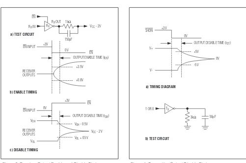
Figure 1. Transmitter Propagation-Delay Timing Figure 2. Receiver Propagation-Delay Timing
EN
RX IN
a) TEST CIRCUIT
b) ENABLE TIMING
c) DISABLE TIMING EN INPUT
RECEIVER OUTPUTS
RX OUT RX
1kΩ
0V
+3V
EN
EN +0.8V +3.5V
OUTPUT ENABLE TIME (tER)
VCC - 2V
VOL + 0.5V VOH - 0.5V
OUTPUT DISABLE TIME (tDR) VCC - 2V
+3V
0V
150pF
EN INPUT
VOH
RECEIVER OUTPUTS
VOL
1 OR 0 TX
3kΩ 50pF -5V
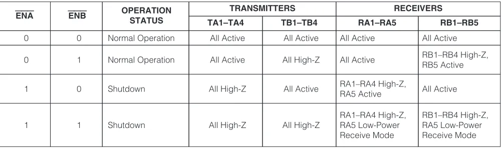
+5V
OUTPUT DISABLE TIME (tDT)
V+ SHDN +3V
0V
V-0V
a) TIMING DIAGRAM
b) TEST CIRCUIT
Figure 3. Receiver-Output Enable and Disable Timing Figure 4. Transmitter-Output Disable Timing
MAX220–MAX249
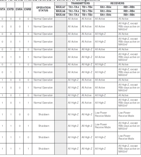
ENT ENR OPERATION STATUS TRANSMITTERS RECEIVERS
0 0 Normal Operation All Active All Active
0 1 Normal Operation All Active All High-Z
1 0 Shutdown All High-Z All Low-Power Receive Mode
1 1 Shutdown All High-Z All High-Z
Table 1a. MAX245 Control Pin Configurations
ENT ENR OPERATION
STATUS
TRANSMITTERS RECEIVERS
TA1–TA4 TB1–TB4 RA1–RA5 RB1–RB5
0 0 Normal Operation All Active All Active All Active All Active
0 1 Normal Operation All Active All Active RA1–RA4 High-Z,
RA5 Active
RB1–RB4 High-Z, RB5 Active
1 0 Shutdown All High-Z All High-Z All Low-Power
Receive Mode
All Low-Power Receive Mode
1 1 Shutdown All High-Z All High-Z
RA1–RA4 High-Z, RA5 Low-Power Receive Mode
RB1–RB4 High-Z, RB5 Low-Power Receive Mode
Table 1b. MAX245 Control Pin Configurations
Table 1c. MAX246 Control Pin Configurations
ENA ENB OPERATION
STATUS
TRANSMITTERS RECEIVERS
TA1–TA4 TB1–TB4 RA1–RA5 RB1–RB5
0 0 Normal Operation All Active All Active All Active All Active
0 1 Normal Operation All Active All High-Z All Active RB1–RB4 High-Z,
RB5 Active
1 0 Shutdown All High-Z All Active RA1–RA4 High-Z,
RA5 Active All Active
1 1 Shutdown All High-Z All High-Z
RA1–RA4 High-Z, RA5 Low-Power Receive Mode
MAX220–MAX249
TA1–TA4 TB1–TB4 RA1–RA4 RB1–RB4
0 0 0 0 Normal Operation All Active All Active All Active All Active
0 0 0 1 Normal Operation All Active All Active All Active
All High-Z, except RB5 stays active on MAX247
0 0 1 0 Normal Operation All Active All Active All High-Z All Active
0 0 1 1 Normal Operation All Active All Active All High-Z
All High-Z, except RB5 stays active on MAX247
0 1 0 0 Normal Operation All Active All High-Z All Active All Active
0 1 0 1 Normal Operation All Active All High-Z All Active
All High-Z, except RB5 stays active on MAX247
0 1 1 0 Normal Operation All Active All High-Z All High-Z All Active
0 1 1 1 Normal Operation All Active All High-Z All High-Z
All High-Z, except RB5 stays active on MAX247
1 0 0 0 Normal Operation All High-Z All Active All Active All Active
1 0 0 1 Normal Operation All High-Z All Active All Active
All High-Z, except RB5 stays active on MAX247
1 0 1 0 Normal Operation All High-Z All Active All High-Z All Active
1 0 1 1 Normal Operation All High-Z All Active All High-Z
All High-Z, except RB5 stays active on MAX247
1 1 0 0 Shutdown All High-Z All High-Z Low-Power
Receive Mode
Low-Power Receive Mode
1 1 0 1 Shutdown All High-Z All High-Z Low-Power
Receive Mode
All High-Z, except RB5 stays active on MAX247
1 1 1 0 Shutdown All High-Z All High-Z All High-Z Low-Power
Receive Mode
1 1 1 1 Shutdown All High-Z All High-Z All High-Z
All High-Z, except RB5 stays active on MAX247
Table 1d. MAX247/MAX248/MAX249 Control Pin Configurations
MAX248 OPERATION
STATUS
ENRB MAX247 TA1–TA4 TB1–TB4 RA1–RA4 RB1–RB5
TRANSMITTERS
ENRA ENTB ENTA
MAX220–MAX249
_______________Detailed Description
The MAX220–MAX249 contain four sections: dual
charge-pump DC-DC voltage converters, RS-232
dri-vers, RS-232 receidri-vers, and receiver and transmitter
enable control inputs.
Dual Charge-Pump Voltage Converter
The MAX220–MAX249 have two internal charge-pumps
that convert +5V to ±10V (unloaded) for RS-232 driver
operation. The first converter uses capacitor C1 to
dou-ble the +5V input to +10V on C3 at the V+ output. The
second converter uses capacitor C2 to invert +10V to
-10V on C4 at the V- output.
A small amount of power may be drawn from the +10V
(V+) and -10V (V-) outputs to power external circuitry
(see the Typical Operating Characteristics section),
except on the MAX225 and MAX245–MAX247, where
these pins are not available. V+ and V- are not regulated,
so the output voltage drops with increasing load current.
Do not load V+ and V- to a point that violates the
mini-mum ±5V EIA/TIA-232E driver output voltage when
sourcing current from V+ and V- to external circuitry.
When using the shutdown feature in the MAX222,
MAX225, MAX230, MAX235, MAX236, MAX240,
MAX241, and MAX245–MAX249, avoid using V+ and
V-to power external circuitry. When these parts are shut
down, V- falls to 0V, and V+ falls to +5V. For
applica-tions where a +10V external supply is applied to the V+
pin (instead of using the internal charge pump to
gen-erate +10V), the C1 capacitor must not be installed and
the
SHDN
pin must be connected to V
CC. This is
because V+ is internally connected to V
CCin shutdown
mode.
RS-232 Drivers
The typical driver output voltage swing is ±8V when
loaded with a nominal 5k
Ω
RS-232 receiver and V
CC=
+5V. Output swing is guaranteed to meet the
EIA/TIA-232E and V.28 specification, which calls for ±5V
mini-mum driver output levels under worst-case conditions.
These include a minimum 3k
Ω
load, V
CC= +4.5V, and
maximum operating temperature. Unloaded driver
out-put voltage ranges from (V+ -1.3V) to (V- +0.5V).
Input thresholds are both TTL and CMOS compatible.
The inputs of unused drivers can be left unconnected
since 400k
Ω
input pullup resistors to V
CCare built in
(except for the MAX220). The pullup resistors force the
outputs of unused drivers low because all drivers invert.
The internal input pullup resistors typically source 12µA,
except in shutdown mode where the pullups are
dis-abled. Driver outputs turn off and enter a
high-imped-ance state—where leakage current is typically
microamperes (maximum 25µA)—when in shutdown
mode, in three-state mode, or when device power is
removed. Outputs can be driven to ±15V. The
power-supply current typically drops to 8µA in shutdown mode.
The MAX220 does not have pullup resistors to force the
outputs of the unused drivers low. Connect unused
inputs to GND or V
CC.
The MAX239 has a receiver three-state control line, and
the MAX223, MAX225, MAX235, MAX236, MAX240,
and MAX241 have both a receiver three-state control
line and a low-power shutdown control. Table 2 shows
the effects of the shutdown control and receiver
three-state control on the receiver outputs.
The receiver TTL/CMOS outputs are in a high-imped-ance, three-state mode whenever the three-state enable line is high (for the MAX225/MAX235/MAX236/MAX239– MAX241), and are also high-impedance whenever the shutdown control line is high.
When in low-power shutdown mode, the driver outputs
are turned off and their leakage current is less than 1µA
with the driver output pulled to ground. The driver output
leakage remains less than 1µA, even if the transmitter
output is backdriven between 0V and (V
CC+ 6V). Below
-0.5V, the transmitter is diode clamped to ground with
1k
Ω
series impedance. The transmitter is also zener
clamped to approximately V
CC+ 6V, with a series
impedance of 1k
Ω
.
The driver output slew rate is limited to less than 30V/µs
as required by the EIA/TIA-232E and V.28
specifica-tions. Typical slew rates are 24V/µs unloaded and
10V/µs loaded with 3
Ω
and 2500pF.
RS-232 Receivers
EIA/TIA-232E and V.28 specifications define a voltage
level greater than 3V as a logic 0, so all receivers invert.
Input thresholds are set at 0.8V and 2.4V, so receivers
respond to TTL level inputs as well as EIA/TIA-232E and
V.28 levels.
The receiver inputs withstand an input overvoltage up
to ±25V and provide input terminating resistors with
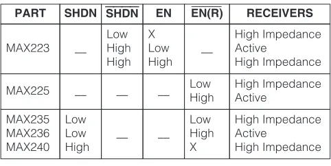
PART SHDN EN EN(R) RECEIVERS
MAX223 __
Low High High
X Low High
High Impedance Active
High Impedance
MAX225 __ __ High Impedance
Active __
MAX235 MAX236 MAX240
Low Low High
__ __
Low High X
High Impedance Active
High Impedance
Table 2. Three-State Control of Receivers
Low High
SHDN
MAX220–MAX249
nominal 5k
Ω
values. The receivers implement Type 1
interpretation of the fault conditions of V.28 and
EIA/TIA-232E.
The receiver input hysteresis is typically 0.5V with a
guaranteed minimum of 0.2V. This produces clear
out-put transitions with slow-moving inout-put signals, even
with moderate amounts of noise and ringing. The
receiver propagation delay is typically 600ns and is
independent of input swing direction.
Low-Power Receive Mode
The low-power receive mode feature of the MAX223,
MAX242, and MAX245–MAX249 puts the IC into
shut-down mode but still allows it to receive information. This
is important for applications where systems are
periodi-cally awakened to look for activity. Using low-power
receive mode, the system can still receive a signal that
will activate it on command and prepare it for
communi-cation at faster data rates. This operation conserves
system power.
Negative Threshold—MAX243
The MAX243 is pin compatible with the MAX232A,
differ-ing only in that RS-232 cable fault protection is removed
on one of the two receiver inputs. This means that control
lines such as CTS and RTS can either be driven or left
unconnected without interrupting communication.
Different cables are not needed to interface with different
pieces of equipment.
The input threshold of the receiver without cable fault
protection is -0.8V rather than +1.4V. Its output goes
positive only if the input is connected to a control line
that is actively driven negative. If not driven, it defaults
to the 0 or “OK to send” state. Normally‚ the MAX243’s
other receiver (+1.4V threshold) is used for the data line
(TD or RD)‚ while the negative threshold receiver is
con-nected to the control line (DTR‚ DTS‚ CTS‚ RTS, etc.).
Other members of the RS-232 family implement the
optional cable fault protection as specified by
EIA/TIA-232E specifications. This means a receiver output goes
high whenever its input is driven negative‚ left
uncon-nected‚ or shorted to ground. The high output tells the
serial communications IC to stop sending data. To
avoid this‚ the control lines must either be driven or
connected with jumpers to an appropriate positive
volt-age level.
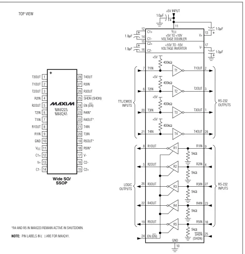
Shutdown—MAX222–MAX242
On the MAX222‚ MAX235‚ MAX236‚ MAX240‚ and
MAX241‚ all receivers are disabled during shutdown.
On the MAX223 and MAX242‚ two receivers continue to
operate in a reduced power mode when the chip is in
shutdown. Under these conditions‚ the propagation
delay increases to about 2.5µs for a high-to-low input
transition. When in shutdown, the receiver acts as a
CMOS inverter with no hysteresis. The MAX223 and
MAX242 also have a receiver output enable input (
EN
for the MAX242 and EN for the MAX223) that allows
receiver output control independent of
SHDN
(SHDN
for MAX241). With all other devices‚
SHDN
(SHDN for
MAX241) also disables the receiver outputs.
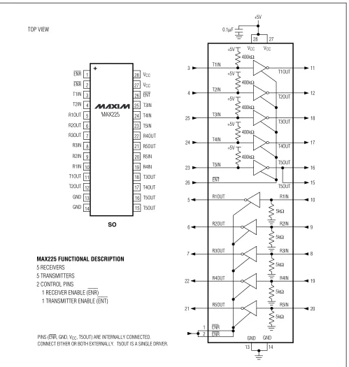
The MAX225 provides five transmitters and five
receivers‚ while the MAX245 provides ten receivers and
eight transmitters. Both devices have separate receiver
and transmitter-enable controls. The charge pumps
turn off and the devices shut down when a logic high is
applied to the ENT input. In this state, the supply
cur-rent drops to less than 25µA and the receivers continue
to operate in a low-power receive mode. Driver outputs
enter a high-impedance state (three-state mode). On
the MAX225‚ all five receivers are controlled by the
ENR
input. On the MAX245‚ eight of the receiver
out-puts are controlled by the
ENR
input‚ while the
remain-ing two receivers (RA5 and RB5) are always active.
RA1–RA4 and RB1–RB4 are put in a three-state mode
when
ENR
is a logic high.
Receiver and Transmitter Enable
Control Inputs
The MAX225 and MAX245–MAX249 feature transmitter
and receiver enable controls.
MAX220–MAX249
Tables 1a–1d define the control states. The MAX244
has no control pins and is not included in these tables.
The MAX246 has ten receivers and eight drivers with
two control pins, each controlling one side of the
device. A logic high at the A-side control input (
ENA
)
causes the four A-side receivers and drivers to go into
a three-state mode. Similarly, the B-side control input
(
ENB
) causes the four B-side drivers and receivers to
go into a three-state mode. As in the MAX245, one
A-side and one B-A-side receiver (RA5 and RB5) remain
active at all times. The entire device is put into
shut-down mode when both the A and B sides are disabled
(
ENA
=
ENB
= +5V).
The MAX247 provides nine receivers and eight drivers
with four control pins. The
ENRA
and
ENRB
receiver
enable inputs each control four receiver outputs. The
ENTA
and
ENTB
transmitter enable inputs each control
four drivers. The ninth receiver (RB5) is always active.
The device enters shutdown mode with a logic high on
both
ENTA
and
ENTB
.
The MAX248 provides eight receivers and eight drivers
with four control pins. The
ENRA
and
ENRB
receiver
enable inputs each control four receiver outputs. The
ENTA
and
ENTB
transmitter enable inputs control four
drivers each. This part does not have an always-active
receiver. The device enters shutdown mode and
trans-mitters go into a three-state mode with a logic high on
both
ENTA
and
ENTB
.
The MAX249 provides ten receivers and six drivers with
four control pins. The
ENRA
and
ENRB
receiver enable
inputs each control five receiver outputs. The
ENTA
and
ENTB
transmitter enable inputs control three
dri-vers each. There is no always-active receiver. The
device enters shutdown mode and transmitters go into
a three-state mode with a logic high on both
ENTA
and
ENTB
. In shutdown mode, active receivers operate in a
MAX220–MAX249
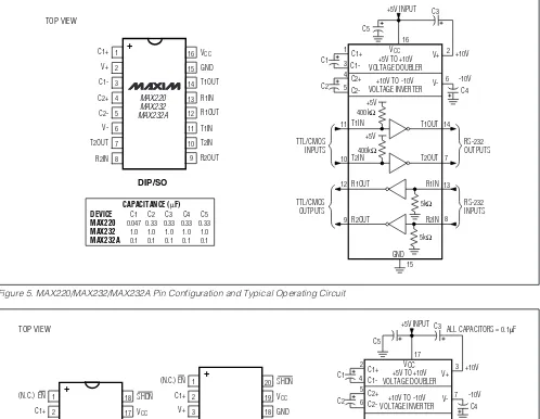
TOP VIEW
16
MAX232A R1OUT
T1IN +5V INPUT
C2+ -10V VOLTAGE INVERTER
+5V TO +10V VOLTAGE DOUBLER
16 C3
C5
CAPACITANCE (µF) DEVICE
9 R2OUT
R2IN
PIN NUMBERS IN TYPICAL OPERATING CIRCUIT ARE FOR DIP/SO PACKAGES ONLY.
V+ (EXCEPT MAX220)
(EXCEPT MAX220)
R1IN T2OUT
R2IN +5V INPUT
C2+ -10V VOLTAGE INVERTER
VCC +5V TO +10V VOLTAGE DOUBLER
17 TOP VIEW
Figure 5. MAX220/MAX232/MAX232A Pin Configuration and Typical Operating Circuit
MAX220–MAX249
13
14
28
27
26
25
24
23
22
21 1
2
3
4
5
6
7
8
VCC
VCC VCC
400kΩ
400kΩ
400kΩ
400kΩ
400kΩ
T1OUT +5V
+5V 0.1µF
+5V
3
28 27
4
25
24
23
26
5
6
7
22
GND ENR
ENR
GND 21
+5V
+5V
+5V
T2OUT
T3OUT
T4OUT
5kΩ
5kΩ
5kΩ
5kΩ
5kΩ
14 13 2
1
T5OUT T5OUT
R1IN
R2IN
R3IN
R4IN
R5IN T1IN
11
12
18
17
16
15
10
9
8
19
20 T2IN
T3IN
T4IN
T5IN
ENT
R2OUT
R3OUT
R4OUT
PINS (ENR, GND, VCC, T5OUT) ARE INTERNALLY CONNECTED.
CONNECT EITHER OR BOTH EXTERNALLY. T5OUT IS A SINGLE DRIVER.
R5OUT R1OUT VCC
ENT
T3IN T2IN
T1IN ENR ENR
T4IN
T5IN
R4OUT
R5OUT R3IN
R3OUT R2OUT R1OUT
20
19
18
17 9
10
11
12
R5IN
R4IN
T3OUT
T4OUT T2OUT
T1OUT R1IN R2IN
SO
MAX225
16
15 T5OUT
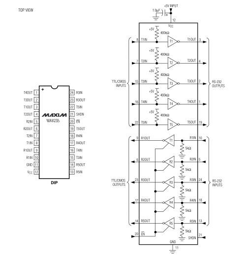
MAX225 FUNCTIONAL DESCRIPTION
5 RECEIVERS 5 TRANSMITTERS 2 CONTROL PINS
1 RECEIVER ENABLE (ENR) 1 TRANSMITTER ENABLE (ENT)
T5OUT GND
GND
TOP VIEW
+
MAX220–MAX249
GND
10
27 R3OUT
23 R4OUT
R3IN
R4IN
5kΩ
5kΩ
5 R2OUT R2IN 4
5kΩ
RS-232 INPUTS LOGIC
OUTPUTS
RS-232 OUTPUTS TTL/CMOS
INPUTS
R2
8 R1OUT R1IN 9
5kΩ
R1
R3
R4
19 R5OUT R5IN 18
5kΩ
R5
2
7 T1IN T1OUT
+5V
400kΩ
+5V
6 T2IN T2OUT 3
T2 400kΩ
20 T3IN T3OUT 1
+5V
T3 400kΩ
C1+
C1-1.0µF
12
VCC
+5V INPUT
11
17
1.0µF 13
1.0µF
+5V TO +10V VOLTAGE DOUBLER
26 1.0µF
T1
28
21 T4IN T4OUT
+5V
400kΩ
T4 14
C2+
C2-15
1.0µF 16
+10V TO -10V VOLTAGE INVERTER
V+
22
EN (EN)
24 25
28
27
26
25
24
23
22
21
20
19
18
17
16
15 1
2
3
4
5
6
7
8
9
10
11
12
13
14
T4OUT
R3IN
R3OUT
SHDN (SHDN)
R4IN*
C2+ R4OUT*
T4IN
T3IN
R5OUT*
R5IN*
V-
C2- C1-V+ C1+ VCC
GND R1IN R1OUT T1IN T2IN R2OUT R2IN T2OUT T1OUT T3OUT
Wide SO/ SSOP
MAX223 MAX241
EN (EN)
SHDN (SHDN) *R4 AND R5 IN MAX223 REMAIN ACTIVE IN SHUTDOWN.
NOTE: PIN LABELS IN ( ) ARE FOR MAX241.
V-+
TOP VIEW
MAX220–MAX249
+5V INPUTC2+ VOLTAGE INVERTER
VCC +5V TO +10V VOLTAGE DOUBLER
7
T3OUT T4OUT
18
N.C. SHDN
T1 +
TOP VIEW
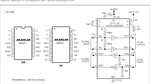
Figure 9. MAX230 Pin Configuration and Typical Operating Circuit
V+
T1IN T1OUT
T2OUT +5V INPUT
RS-232 VOLTAGE CONVERTER
13 (15)
TOP VIEW
MAX220–MAX249
T1IN T1OUT
T2OUT +5V INPUT
RS-232 INPUTS TTL/CMOS
OUTPUTS
GND GND
6 9
T2IN R2OUT
C1+ DO NOT MAKE
CONNECTIONS TO THESE PINS
INTERNAL -10V POWER SUPPLY
INTERNAL +10V POWER SUPPLY
1.0µF TOP VIEW
+
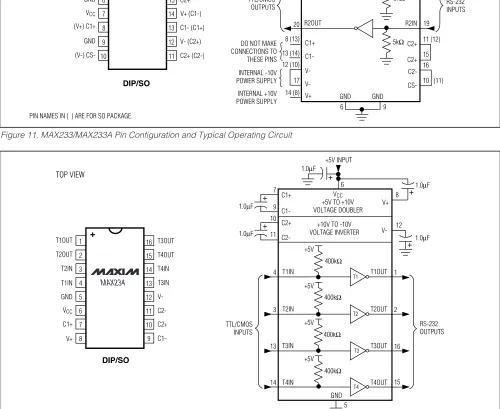
Figure 11. MAX233/MAX233A Pin Configuration and Typical Operating Circuit
16 +5V INPUT
C2-VOLTAGE INVERTER
VCC
+5V TO +10V VOLTAGE DOUBLER
6 TOP VIEW
MAX220–MAX249
1.0µF
+5V INPUT
GND
11 6
23
5 R2OUT
RS-232 INPUTS TTL/CMOS
OUTPUTS
14 13
21 R5OUT
5kΩ
17 R4OUT 18
5kΩ
24 R3OUT
5kΩ
24
23
22
21
20
19
18
17 1
2
3
4
5
6
7
8
R3IN
R3OUT
T5IN
SHDN T2OUT
T1OUT T3OUT T4OUT
EN
T5OUT
R4IN
R4OUT T1IN
T2IN R2OUT R2IN
16
15
14
13 9
10
11
12
T4IN
T3IN
R5OUT
R5IN VCC
GND R1IN R1OUT
DIP
MAX235
5kΩ
9 R1OUT R1IN 10
R2IN
R3IN
R4IN
R5IN 5kΩ
7
15
3
4 T2IN
T3OUT RS-232 OUTPUTS TTL/CMOS
INPUTS
22 T5IN T5OUT 19
+5V
16 T4IN T4OUT 1
+5V
2 T3IN
+5V +5V
8 T1IN T1OUT
+5V
T2OUT T1
T1
R2
R3
R4
R5 T2
T3
T5 T4 400kΩ
400kΩ
400kΩ
400kΩ
400kΩ
SHDN EN
20
12
VCC
+
TOP VIEW
MAX220–MAX249
GND
8
23
R2OUT RS-232
INPUTS TTL/CMOS
OUTPUTS
17 16
21 R3OUT
R2IN
R3IN
5kΩ
5kΩ
5 R1OUT R1IN 4
5kΩ
RS-232 OUTPUTS TTL/CMOS
INPUTS
R1
R2
R3
2
7 T1IN T1OUT
+5V
T1 400kΩ
6 T2IN 3
+5V
T2OUT T2
400kΩ
18 T3IN T3OUT 1
+5V
T3 400kΩ
19 T4IN T4OUT 24
+5V
T4 400kΩ
SHDN EN
20
11 C1+
C1-1.0µF
10
12
13
14
15 +5V INPUT
C2+
C2-VCC
+5V TO +10V VOLTAGE DOUBLER
9 1.0µF
1.0µF +10V TO -10V
VOLTAGE INVERTER
22 24
23
22
21
20
19
18
17 1
2
3
4
5
6
7
8
T4OUT
R2IN
R2OUT
SHDN R1IN
T2OUT T1OUT T3OUT
T4IN
T3IN
R3OUT GND
T1IN T2IN R1OUT
16
15
14
13 9
10
11
12
R3IN
V-
C2-C2+
C1-V+ C1+ VCC
DIP/SO
MAX236 EN
1.0µF
1.0µF
TOP VIEW
V+
V-+
MAX220–MAX249
GND
8
23
R2OUT RS-232
INPUTS TTL/CMOS
OUTPUTS
17 R3OUT 16
R2IN
R3IN
5kΩ
5kΩ
5 R1OUT R1IN 4
5kΩ
RS-232 OUTPUTS TTL/CMOS
INPUTS
R1
R2
R3
2
7 T1IN T1OUT
+5V
T1 400kΩ
6 T2IN 3
+5V
T2OUT T2
400kΩ
18 T3IN T3OUT 1
+5V
T3 400kΩ
21 T5IN T5OUT 20
+5V
T5 400kΩ
11 C1+
C1-1.0µF
10
12
13
14
15 +5V INPUT
C2+
C2-VCC
+5V TO +10V VOLTAGE DOUBLER
9 1.0µF
1.0µF +10V TO -10V
VOLTAGE INVERTER
22 24
23
22
21
20
19
18
17 1
2
3
4
5
6
7
8
T4OUT
R2IN
R2OUT
T5IN R1IN
T2OUT T1OUT T3OUT
T4IN
T3IN
R3OUT GND
T1IN T2IN R1OUT
16
15
14
13 9
10
11
12
R3IN
V-
C2-C2+
C1-V+ C1+ VCC
DIP/SO
MAX237 T5OUT
1.0µF
1.0µF
19 T4IN T4OUT 24
+5V
T4 400kΩ
V+
V-+
TOP VIEW
MAX220–MAX249
GND
8
3 R2OUT
22 R3OUT 23
R2IN
R3IN
5kΩ
5kΩ
6 R1OUT R1IN 7
5kΩ
RS-232 OUTPUTS TTL/CMOS
INPUTS
RS-232 INPUTS TTL/CMOS
OUTPUTS
R1
R2
R3
17 R4OUT R4IN 16
5kΩ
R4
2
5 T1IN T1OUT
+5V 400kΩ
+5V
18 T2IN T2OUT 1
T2 400kΩ
19 T3IN T3OUT 24
+5V
T3 400kΩ
11 C1+
C1-1.0µF
10
12
13
14
15 +5V INPUT
C2+
C2-VCC
+5V TO +10V VOLTAGE DOUBLER
9 1.0µF
1.0µF +10V TO -10V
VOLTAGE INVERTER
4 1.0µF
1.0µF
21 T4IN T4OUT 20
+5V
T4 400kΩ
T1 24
23
22
21
20
19
18
17 1
2
3
4
5
6
7
8
T3OUT
R3IN
R3OUT
T4IN R2OUT
R2IN T1OUT T2OUT
TOP VIEW
T3IN
T2IN
R4OUT GND
R1IN R1OUT T1IN
16
15
14
13 9
10
11
12
R4IN
V-
C2-C2+
C1-V+ C1+ VCC
DIP/SO
MAX238 T4OUT
+
V+
MAX220–MAX249
GND
3
18 R3OUT
12 R4OUT
R3IN
R4IN
5kΩ
5kΩ
22 R2OUT R2IN 21
5kΩ
RS-232 OUTPUTS TTL/CMOS
INPUTS
RS-232 INPUTS TTL/CMOS
OUTPUTS
R2
1 R1OUT R1IN 2
5kΩ
R1
R3
R4
10 R5OUT R5IN 9
5kΩ
R5
19
24 T1IN T1OUT
+5V 400kΩ
+5V
23 T2IN T2OUT 20
T2 400kΩ
16 T3IN T3OUT 13
+5V
T3 400kΩ
C1+
C1-1.0µF
6 VCC 8
+5V INPUT
4 5
1.0µF +10V TO -10V
VOLTAGE INVERTER
17 1.0µF
T1
24
23
22
21
20
19
18
17 1
2
3
4
5
6
7
8
T1IN
T2IN
R2OUT
R2IN VCC
GND R1IN R1OUT
T1OUT
R3IN
R3OUT
V- C-C+ V+
16
15
14
13 9
10
11
12
T3IN
N.C.
EN
T3OUT R4IN
R4OUT R5OUT R5IN
DIP/SO
MAX239 T2OUT
+7.5V TO +13.2V INPUT
7
V+
11
EN
14 15
N.C.
V-+
TOP VIEW
MAX220–MAX249
13 R2OUT R2IN 10
5kΩ
16 R1OUT R1IN 17
5kΩ
R1
R3
R4
36 R5OUT R5IN 35
5kΩ
R5
7
15 T1IN T1OUT
+5V 400kΩ
+5V
14 T2IN T2OUT 8
T2 400kΩ
37 T3IN T3OUT 6
+5V +5V INPUT
19 VOLTAGE DOUBLER
3 1.0µF
T1
+5V
2 T5IN T5OUT 41
T5 400kΩ
5
38 T4IN T4OUT
+5V VOLTAGE INVERTER
V+
39
EN
42 43
Plastic FP
MAX240
R2IN N.C. T2OUT T1OUT T3OUT T4OUT
N.C. R3IN R3OUT T5IN N.C.
N.C. C1+ V+ C1- C2+ C2
TOP VIEW
V-+
MAX220–MAX249
V+
V-2 +10V C1+
C1-1
3
4
5
11
10
12
9
6
14
7
13
8 T1IN
R1OUT T2IN
R2OUT
T1OUT
R1IN T2OUT
R2IN +5V INPUT
C2+
C2--10V
RS-232 OUTPUTS
RS-232 INPUTS TTL/CMOS
INPUTS
TTL/CMOS OUTPUTS
GND
15 5kΩ
5kΩ
400kΩ
400kΩ
+5V
+5V
+10V TO -10V VOLTAGE INVERTER
+5V TO +10V VOLTAGE DOUBLER
16
16
15
14
13
12
11
10
9 1
2
3
4
5
6
7
8
C1+ VCC
GND
T1OUT
R1IN
R1OUT
T1IN
T2IN
R2OUT MAX243
DIP/SO
V+
C1- V-C2+
C2-T2OUT
R2IN
0.1µF
0.1µF
0.1µF 0.1µF
0.1µF
RECEIVER INPUT
≤ -3V OPEN
≥ +3V
R1 OUTPUT HIGH HIGH LOW
R2 OUTPUT HIGH LOW LOW
TOP VIEW
VCC
+
MAX220–MAX249
400kΩ
+10V TO -10V VOLTAGE INVERTER +5V TO +10V VOLTAGE DOUBLER
VCC
9 RA1IN
10 RA1OUT
8 RA2IN
11 RA2OUT
7 RA3IN
12 RA3OUT
6 RA4IN
13 RA4OUT
5 RA5IN
14 MAX249 FUNCTIONAL DESCRIPTION
10 RECEIVERS 5 A-SIDE RECEIVERS 5 B-SIDE RECEIVERS 8 TRANSMITTERS 4 A-SIDE TRANSMITTERS 4 B-SIDE TRANSMITTERS NO CONTROL PINS
44 TOP VIEW
TA4OUT TA3OUT TA2OUT TA1OUT TB1OUT TB2OUT TB3OUT TB4OUT RB5IN
GND C1+ V+ C1- C2+ C2- V- TB4IN TB3IN
MAX220–MAX249
11 RA1IN
10 RA1OUT
12 RA2IN
9 RA2OUT
13 RA3IN
8 RA3OUT
14 RA4IN
7 RA4OUT
15 RA5IN
6
RA4OUT
RA3OUT
RA2OUT
RA1OUT
RA1IN
RA2IN
RA3IN
RA4IN
RA5IN
TA1OUT
TA2OUT
TA3OUT
TA4OUT
GND
TOP VIEW
MAX245
MAX245 FUNCTIONAL DESCRIPTION
10 RECEIVERS
5 A-SIDE RECEIVERS (RA5 ALWAYS ACTIVE) 5 B-SIDE RECEIVERS (RB5 ALWAYS ACTIVE) 8 TRANSMITTTERS
4 A-SIDE TRANSMITTERS 2 CONTROL PINS
1 RECEIVER ENABLE (ENR) 1 TRANSMITTER ENABLE (ENT)
39
+
ENR ENT
MAX220–MAX249
11 RA1IN
10 RA1OUT
12 RA2IN
9 RA2OUT
13 RA3IN
8 RA3OUT
14 RA4IN
7 RA4OUT
15 RA5IN
6 RA5OUT
29
RA4OUT
RA3OUT
RA2OUT
RA1OUT
RA1IN
RA2IN
RA3IN
RA4IN
RA5IN
TA1OUT
TA2OUT
TA3OUT
TA4OUT
GND
TOP VIEW
MAX246
MAX246 FUNCTIONAL DESCRIPTION
10 RECEIVERS
5 A-SIDE RECEIVERS (RA5 ALWAYS ACTIVE) 5 B-SIDE RECEIVERS (RB5 ALWAYS ACTIVE) 8 TRANSMITTERS
4 A-SIDE TRANSMITTERS 4 B-SIDE TRANSMITTERS 2 CONTROL PINS
ENABLE A-SIDE (ENA) ENABLE B-SIDE (ENB)
ENA ENB
+
MAX220–MAX249
6 RB5OUT
12 RA1IN
10 RA1OUT
13 RA2IN
9 RA2OUT
14 RA3IN
8 RA3OUT
15 RA4IN
7
RA4OUT
RA3OUT
RA2OUT
RA1OUT
RA1IN
RA2IN
RA3IN
RA4IN
TA1OUT
TA2OUT
TA3OUT
TA4OUT
GND
TOP VIEW
MAX247
MAX247 FUNCTIONAL DESCRIPTION
9 RECEIVERS
4 A-SIDE RECEIVERS
5 B-SIDE RECEIVERS (RB5 ALWAYS ACTIVE) 8 TRANSMITTERS
4 A-SIDE TRANSMITTERS 4 B-SIDE TRANSMITTERS 4 CONTROL PINS
ENABLE RECEIVER A-SIDE (ENRA) ENABLE RECEIVER B-SIDE (ENRB) ENABLE RECEIVER A-SIDE (ENTA) ENABLE RECEIVER B-SIDE (ENTB)
+
MAX220–MAX249
400kΩ
+10V TO -10V VOLTAGE INVERTER +5V TO +10V VOLTAGE DOUBLER
VCC
8 RA1IN
10 RA1OUT
7 RA2IN
11 RA2OUT
6 RA3IN
12 RA3OUT
5 RA4IN
13 TOP VIEW
TA4OUT TA3OUT TA2OUT TA1OUT TB1OUT TB2OUT TB3OUT TA4OUT RB4IN
GND C1+ V+ C1- C2+ C2- V- ENTB TB4IN
MAX248 FUNCTIONAL DESCRIPTION
8 RECEIVERS
4 A-SIDE RECEIVERS 4 B-SIDE RECEIVERS 8 TRANSMITTERS
4 A-SIDE TRANSMITTERS 4 B-SIDE TRANSMITTERS 4 CONTROL PINS
ENABLE RECEIVER A-SIDE (ENRA) ENABLE RECEIVER B-SIDE (ENRB) ENABLE RECEIVER A-SIDE (ENTA) ENABLE RECEIVER B-SIDE (ENTB
)
+
MAX220–MAX249
400kΩ
+10V TO -10V VOLTAGE INVERTER +5V TO +10V VOLTAGE DOUBLER
VCC
8 RA1IN
10 RA1OUT
7 RA2IN
11 RA2OUT
6 RA3IN
12 RA3OUT
5 RA4IN
13 RA4OUT
4 RA5IN
14
RA4IN RA5IN
MAX249
PLCC TOP VIEW
TA3OUT TA2OUT TA1OUT TB1OUT TB2OUT TB3OUT RB5IN RB4IN
GND C1+ V+ C1- C2+ C2-
V-MAX249 FUNCTIONAL DESCRIPTION
10 RECEIVERS 5 A-SIDE RECEIVERS 5 B-SIDE RECEIVERS 6 TRANSMITTERS
3 A-SIDE TRANSMITTERS 3 B-SIDE TRANSMITTERS 4 CONTROL PINS
ENABLE RECEIVER A-SIDE (ENRA)
MAX220–MAX249
___________________________________________Ordering Information (continued)
PART
MAX222CPN+ 0°C to +70°C
TEMP RANGE PIN-PACKAGE PART TEMP RANGE PIN-PACKAGE
18 Plastic DIP
MAX222CWN+ 0°C to +70°C 18 Wide SO
MAX222C/D 0°C to +70°C Dice*
MAX222EPN+ -40°C to +85°C 18 Plastic DIP
MAX222EWN+ -40°C to +85°C 18 Wide SO
MAX222EJN -40°C to +85°C 18 CERDIP
MAX222MJN -55°C to +125°C 18 CERDIP
MAX223CAI+ 0°C to +70°C 28 SSOP
MAX223CWI+ 0°C to +70°C 28 Wide SO
MAX223C/D 0°C to +70°C Dice*
MAX223EAI+ -40°C to +85°C 28 SSOP
MAX223EWI+ -40°C to +85°C 28 Wide SO
MAX225CWI+ 0°C to +70°C 28 Wide SO
MAX225EWI+ -40°C to +85°C 28 Wide SO
MAX230CPP+ 0°C to +70°C 20 Plastic DIP
MAX230CWP+ 0°C to +70°C 20 Wide SO
MAX230C/D 0°C to +70°C Dice*
MAX230EPP+ -40°C to +85°C 20 Plastic DIP
MAX230EWP+ -40°C to +85°C 20 Wide SO
MAX230EJP -40°C to +85°C 20 CERDIP
MAX230MJP -55°C to +125°C 20 CERDIP
MAX231CPD+ 0°C to +70°C 14 Plastic DIP
MAX231CWE+ 0°C to +70°C 16 Wide SO
MAX231CJD 0°C to +70°C 14 CERDIP
MAX231C/D 0°C to +70°C Dice*
MAX231EPD+ -40°C to +85°C 14 Plastic DIP
MAX231EWE+ -40°C to +85°C 16 Wide SO
MAX231EJD -40°C to +85°C 14 CERDIP
MAX231MJD -55°C to +125°C 14 CERDIP
MAX232CPE+ 0°C to +70°C 16 Plastic DIP
MAX232CSE+ 0°C to +70°C 16 Narrow SO
MAX232CWE+ 0°C to +70°C 16 Wide SO
MAX232C/D 0°C to +70°C Dice*
MAX232EPE+ -40°C to +85°C 16 Plastic DIP
MAX232ESE+ -40°C to +85°C 16 Narrow SO
MAX232EWE+ -40°C to +85°C 16 Wide SO
MAX232EJE -40°C to +85°C 16 CERDIP
MAX232MJE -55°C to +125°C 16 CERDIP
MAX232MLP+ -55°C to +125°C 20 LCC
MAX232ACPE+ 0°C to +70°C 16 Plastic DIP
MAX232ACSE+ 0°C to +70°C 16 Narrow SO
MAX232ACWE+ 0°C to +70°C 16 Wide SO
MAX232AC/D
MAX232AEPE+ -40°C to +85°C 16 Plastic DIP MAX232AESE+
0°C to +70°C Dice*
-40°C to +85°C 16 Narrow SO
MAX232AEWE+ -40°C to +85°C 16 Wide SO
MAX232AEJE -40°C to +85°C 16 CERDIP
MAX232AMJE -55°C to +125°C 16 CERDIP
MAX232AMLP+ -55°C to +125°C 20 LCC
MAX233CPP+ 0°C to +70°C 20 Plastic DIP
MAX233EPP+ -40°C to +85°C 20 Plastic DIP
MAX233ACPP+ 0°C to +70°C 20 Plastic DIP
MAX233ACWP+ 0°C to +70°C 20 Wide SO
MAX233AEPP+ -40°C to +85°C 20 Plastic DIP
MAX233AEWP+ -40°C to +85°C 20 Wide SO
MAX234CPE+ 0°C to +70°C 16 Plastic DIP
MAX234CWE+ 0°C to +70°C 16 Wide SO
MAX234C/D 0°C to +70°C Dice*
MAX234EPE+ -40°C to +85°C 16 Plastic DIP
MAX234EWE+ -40°C to +85°C 16 Wide SO
MAX234EJE -40°C to +85°C 16 CERDIP
MAX234MJE -55°C to +125°C 16 CERDIP
MAX235CPG+ 0°C to +70°C 24 Wide Plastic DIP
MAX235EPG+ -40°C to +85°C 24 Wide Plastic DIP
MAX235EDG -40°C to +85°C 24 Ceramic SB
MAX235MDG -55°C to +125°C 24 Ceramic SB
MAX236CNG+ 0°C to +70°C 24 Narrow Plastic DIP
MAX236CWG+ 0°C to +70°C 24 Wide SO
MAX236C/D 0°C to +70°C Dice*
MAX236ENG+ -40°C to +85°C 24 Narrow Plastic DIP
MAX236EWG+ -40°C to +85°C 24 Wide SO
MAX236ERG -40°C to +85°C 24 Narrow CERDIP
MAX236MRG -55°C to +125°C 24 Narrow CERDIP
MAX237CNG+ 0°C to +70°C 24 Narrow Plastic DIP
MAX237CWG+ 0°C to +70°C 24 Wide SO
MAX237C/D 0°C to +70°C Dice*
MAX237ENG+ -40°C to +85°C 24 Narrow Plastic DIP
MAX237EWG+ -40°C to +85°C 24 Wide SO
MAX237ERG -40°C to +85°C 24 Narrow CERDIP
MAX237MRG -55°C to +125°C 24 Narrow CERDIP
MAX238CNG+ 0°C to +70°C 24 Narrow Plastic DIP
MAX238CWG+ 0°C to +70°C 24 Wide SO
MAX238C/D 0°C to +70°C Dice*
MAX220–MAX249
MAX238ENG+ -40°C to +85°C 24 Narrow Plastic DIP
___________________________________________Ordering Information (continued)
18 CERDIP -55°C to +125°C
MAX242MJN
18 CERDIP -40°C to +85°C
MAX242EJN
18 Wide SO -40°C to +85°C
MAX242EWN+
18 Plastic DIP -40°C to +85°C
18 Plastic DIP 0°C to +70°C
MAX242CPN+
20 SSOP 0°C to +70°C
MAX242CAP+
28 Wide SO -40°C to +85°C
MAX241EWI+
28 SSOP -40°C to +85°C
28 SSOP 0°C to +70°C
MAX241CAI+
Dice* 0°C to +70°C
MAX240C/D
44 Plastic FP 0°C to +70°C
MAX240CMH+
24 Narrow CERDIP -55°C to +125°C
MAX239MRG
24 Narrow CERDIP -40°C to +85°C
MAX239ERG
24 Wide SO -40°C to +85°C
MAX239EWG+
24 Narrow Plastic DIP -40°C to +85°C
24 Narrow Plastic DIP 0°C to +70°C
MAX239CNG+
24 Narrow CERDIP -55°C to +125°C
24 Wide SO
PIN-PACKAGE TEMP RANGE
-40°C to +85°C
MAX238MRG
24 Narrow CERDIP -40°C to +85°C
MAX238ERG MAX238EWG+
PART PART TEMP RANGE PIN-PACKAGE
44 PLCC -40°C to +85°C
MAX249EQH+
44 PLCC 0°C to +70°C
MAX249CQH+
44 PLCC -40°C to +85°C
MAX248EQH+
Dice* 0°C to +70°C
MAX248C/D
44 PLCC 0°C to +70°C
MAX248CQH+
40 Plastic DIP -40°C to +85°C
MAX247EPL+
Dice* 0°C to +70°C
MAX247C/D
40 Plastic DIP 0°C to +70°C
MAX247CPL+
40 Plastic DIP -40°C to +85°C
MAX246EPL+
Dice* 0°C to +70°C
MAX246C/D
40 Plastic DIP 0°C to +70°C
MAX246CPL+
40 Plastic DIP -40°C to +85°C
MAX245EPL+
Dice* 0°C to +70°C
MAX245C/D
40 Plastic DIP 0°C to +70°C
MAX245CPL+
44 PLCC -40°C to +85°C
MAX244EQH+
Dice* 0°C to +70°C
MAX244C/D
44 PLCC 0°C to +70°C
MAX244CQH+
16 CERDIP -55°C to +125°C
MAX243MJE
16 CERDIP -40°C to +85°C
MAX243EJE
16 Wide SO -40°C to +85°C
MAX243EWE+
16 Narrow SO -40°C to +85°C
MAX243ESE+
16 Plastic DIP -40°C to +85°C
16 Plastic DIP 0°C to +70°C
MAX243CWE+
16 Narrow SO 0°C to +70°C
MAX243CSE+
MAX243CPE+
MAX220–MAX249
Package Information
For the latest package outline information and land patterns, go to www.maxim-ic.com/packages. Note that a “+”, “#”, or “-” in the package code indicates RoHS status only. Package drawings may show a different suffix character, but the drawing pertains to the package regardless of RoHS status.PACKAGE TYPE PACKAGE CODE OUTLINE NO. LAND PATTERN NO.
14 PDIP P14+3
21-0043
—
16 PDIP P16+1
16 PDIP P16+2
16 PDIP P16+3
18 PDIP P18+5
20 PDIP P20+3
20 PDIP P20M+1
24 PDIP N24+3
24 PDIP P24M+1
21-0044
28 PDIP P28+2
40 PDIP P40+1
40 PDIP P40M+2
14 CERDIP J14-3
21-0045
16 CERDIP J16-3
18 CERDIP J18-2
20 CERDIP J20-2
24 CERDIP R24-4
16 SO(N) S16+3
21-0041 90-0097
16 SO(N) S16+5
16 SO(W) W16+1
21-0042
90-0107
16 SO(W) W16+2
16 SO(W) W16+3
18 SO(W) W18+1 90-0181
20 SO(W) W20+3
90-0108
20 SO(W) W20M+1
24 SO(W) W24+2 90-0182
28 SO(W) W28+1
90-0109
28 SO(W) W28+2
28 SO(W) W28M+1
20 LCC L20+3 21-0658 90-0177
20 SSOP A20+1
21-0056
90-0094
24 SSOP A24+2 90-0110
28 SSOP A28+1 90-0095
16 TSSOP U16+1 90-0117
16 FPCK F16-3 21-0013 —
44 MQFP M44+5 21-0826 90-0169
44 PLCC Q44+1
21-0049 90-0236