INTRODUCTION TO
DIGITAL SYSTEMS
Modeling, Synthesis, and Simulation
Using VHDL
Mohammed Ferdjallah
The Virginia Modeling, Analysis and Simulation Center Old Dominion University
Suffolk, Virginia
CopyrightÓ2011 by John Wiley & Sons, Inc. All rights reserved. Published by John Wiley & Sons, Inc., Hoboken, New Jersey. Published simultaneously in Canada.
No part of this publication may be reproduced, stored in a retrieval system, or transmitted in any form or by any means, electronic, mechanical, photocopying, recording, scanning, or otherwise, except as permitted under Sections 107 or 108 of the 1976 United States Copyright Act, without either the prior written permission of the Publisher, or authorization through payment of the appropriate per-copy fee to the Copyright Clearance Center, Inc., 222 Rosewood Drive, Danvers, MA 01923, (978) 750-8400, fax (978) 750-4470, or on the web at www.copyright.com. Requests to the Publisher for permission should be addressed to the Permissions Department, John Wiley & Sons, Inc., 111 River Street, Hoboken, NJ 07030, (201) 748-6011, fax (201) 748-6008, or online at http://www.wiley.com/go/permission. Limit of Liability/Disclaimer of Warranty: While the publisher and author have used their best efforts in preparing this book, they make no representations or warranties with respect to the accuracy or completeness of the contents of this book and specifically disclaim any implied warranties of merchantability or fitness for a particular purpose. No warranty may be created or extended by sales representatives or written sales materials. The advice and strategies contained herein may not be suitable for your situation. You should consult with a professional where appropriate. Neither the publisher nor author shall be liable for any loss of profit or any other commercial damages, including but not limited to special, incidental, consequential, or other damages.
For general information on our other products and services or for technical support, please contact our Customer Care Department within the United States at (800) 762-2974, outside the United States at (317) 572-3993 or fax (317) 572-4002.
Wiley also publishes its books in a variety of electronic formats. Some content that appears in print may not be available in electronic formats. For more information about Wiley products, visit our web site at www.wiley.com.
Library of Congress Cataloging-in-Publication Data: Ferdjallah, Mohammed.
Introduction to digital systems : modeling, synthesis, and simulation using VHDL / Mohammed Ferdjallah.
p. cm.
Includes bibliographical references and index. ISBN 978-0-470-90055-0 (cloth)
1. Digital electronics. 2. Digital electronics–Computer simulation. 3. VHDL (Computer hardware description language) I. Title.
TK7868.D5F47 2011
621.39’2–dc22 2010041036
CONTENTS
Preface ix
1 Digital System Modeling and Simulation 1
1.1 Objectives 1
1.2 Modeling, Synthesis, and Simulation Design 1 1.3 History of Digital Systems 2
1.4 Standard Logic Devices 2
1.5 Custom-Designed Logic Devices 3 1.6 Programmable Logic Devices 3 1.7 Simple Programmable Logic Devices 4 1.8 Complex Programmable Logic Devices 5 1.9 Field-Programmable Gate Arrays 6 1.10 Future of Digital Systems 7 Problems 8
2 Number Systems 9
2.1 Objectives 9
2.2 Bases and Number Systems 9 2.3 Number Conversions 11 2.4 Data Organization 13
2.5 Signed and Unsigned Numbers 13 2.6 Binary Arithmetic 16
2.7 Addition of Signed Numbers 17
2.8 Binary-Coded Decimal Representation 19 2.9 BCD Addition 20
Problems 21
3 Boolean Algebra and Logic 24
3.1 Objectives 24 3.2 Boolean Theory 24
3.3 Logic Variables and Logic Functions 25 3.4 Boolean Axioms and Theorems 25 3.5 Basic Logic Gates and Truth Tables 27 3.6 Logic Representations and Circuit Design 27
3.7 Truth Table 28 3.8 Timing Diagram 31 3.9 Logic Design Concepts 31 3.10 Sum-of-Products Design 32 3.11 Product-of-Sums Design 33 3.12 Design Examples 34
3.13 NAND and NOR Equivalent Circuit Design 36 3.14 Standard Logic Integrated Circuits 37
Problems 39
4 VHDL Design Concepts 46
4.1 Objectives 46
4.2 CAD Tool–Based Logic Design 46 4.3 Hardware Description Languages 47 4.4 VHDL Language 48
4.5 VHDL Programming Structure 48 4.6 Assignment Statements 51 4.7 VHDL Data Types 51 4.8 VHDL Operators 55
4.9 VHDL Signal and Generate Statements 56 4.10 Sequential Statements 58
4.11 Loops and Decision-Making Statements 59 4.12 Subcircuit Design 61
4.13 Packages and Components 61 Problems 64
5 Integrated Logic 68
5.1 Objectives 68 5.2 Logic Signals 68 5.3 Logic Switches 69
5.4 NMOS and PMOS Logic Gates 70 5.5 CMOS Logic Gates 72
5.6 CMOS Logic Networks 75
5.7 Practical Aspects of Logic Gates 76 5.8 Transmission Gates 79
Problems 81
6 Logic Function Optimization 87
6.1 Objectives 87
6.2 Logic Function Optimization Process 87 6.3 Karnaugh Maps 87
6.6 Four-Variable Karnaugh Map 91 6.7 Five-Variable Karnaugh Map 93 6.8 XOR and NXOR Karnaugh Maps 94 6.9 Incomplete Logic Functions 94 6.10 Quine–McCluskey Minimization 96 Problems 99
7 Combinational Logic 105
7.1 Objectives 105
7.2 Combinational Logic Circuits 105 7.3 Multiplexers 106
7.4 Logic Design with Multiplexers 111 7.5 Demultiplexers 112
7.6 Decoders 113 7.7 Encoders 115 7.8 Code Converters 116 7.9 Arithmetic Circuits 120 Problems 129
8 Sequential Logic 133
8.1 Objectives 133
8.2 Sequential Logic Circuits 133 8.3 Latches 134
8.4 Flip-Flops 138 8.5 Registers 145 8.6 Counters 149 Problems 158
9 Synchronous Sequential Logic 165
9.1 Objectives 165
9.2 Synchronous Sequential Circuits 165 9.3 Finite-State Machine Design Concepts 167 9.4 Finite-State Machine Synthesis 171 9.5 State Assignment 178
9.6 One-Hot Encoding Method 180 9.7 Finite-State Machine Analysis 182 9.8 Sequential Serial Adder 184 9.9 Sequential Circuit Counters 188 9.10 State Optimization 195
9.11 Asynchronous Sequential Circuits 199 Problems 201
Index 213
PREFACE
Digital system design requires rigorous modeling and simulation analysis that eliminates design risks and potential harm to users. Thus, the educational objective of this book is to provide an introduction to digital system design through modeling, synthesis, and simulation computer-aided design (CAD) tools. This book provides an introduction to analytical and computational methods that allow students and users to model, synthesize, and simulate digital principles using very high-speed integrated-circuit hardware description language (VHDL) programming. We present the prac-tical application of modeling and synthesis to digital system design to establish a basis for effective design and provide a systematic tutorial of how basic digital systems function. In doing so, we integrate theoretical principles, discrete mathematical models, computer simulations, and basics methods of analysis. Students and users will learn how to use modeling, synthesis, and simulation concepts and CAD tools to design models for digital systems that will allow them to gain insights into their functions and the mechanisms of their control. Students will learn how to integrate basic models into more complex digital systems. Although the approach designed in this book focuses on undergraduate students, it can also be used for modeling and simulation students who have a limited engineering background with an inclination to digital systems for visualization purposes.
The book includes nine chapters. Each chapter begins with learning objectives that provide a brief overview of the concepts that the reader is about to learn. In addition, the learning objectives can be used as points for classroom discussion. Each chapter ends with problems that will enable students to practice and review the concepts covered in the chapter. Chapter 1 introduces modeling and simulation and its role in digital system evolution. The chapter provides a brief history of modeling and simula-tion in digital systems, VHDL programming, programmable and reconfigurable systems, and advantages of using modeling and simulation in digital system design. Chapter 2 introduces the mathematical foundations of digital systems and logical reasoning. Described are Boolean theory, its axioms and theorems, and basic logic gates as well as early modeling in digital system design using algebraic manipulations.
Chapter 3 provides an overview of number representations, number conversions, and number codes. The relationships between decimal representation and the less obvious digital number representations are described. Chapter 4 provides a brief history of VHDL programming, the reasons for its creation, and its impact on the evolution of digital systems and modern computer systems. Described are CAD tools, programming structure, and instructions and syntax of VHDL. Chapter 5 provides a simplified view of the progression of integrated systems and their application in
digital logic circuits and computer systems. The role of modeling and simulation in the optimization and verification of digital system design at the transistor level is described. Chapter 6 provides graphical means and Karnaugh maps to streamline and simplify digital system design using visualization schemes. Although these methods are used only when designing circuits with a small number of gates, they provide rudimentary means for the design of automatic CAD tools.
Chapter 7 introduces combinational logic and its applications in multiplexers, decoders, and arithmetic and logic circuits and systems. Chapter 8 introduces sequen-tial logic, with a focus on sequensequen-tial logic elementary circuits and their applications in complex circuits such as counters and registers. Chapter 9 provides an overview of finite-state machines, especially the synchronous sequential circuit models used to design simple finite-state machines. Also described is asynchronous sequential logic and its advantages and disadvantages for digital systems. All chapters illustrate circuit design using VHDL sample codes that allow students not only to learn and master VHDL programming but also to model and simulate digital circuits.
MOHAMMEDFERDJALLAH
1
Digital System Modeling
and Simulation
1.1 OBJECTIVES
The objectives of the chapter are to:
. Describe digital systems
. Provide a brief history of digital systems
. Describe standard chips
. Describe custom-designed chips
. Describe programmable logic devices
. Describe field-programmable gated arrays
1.2 MODELING, SYNTHESIS, AND SIMULATION DESIGN
Modeling and simulation have their roots in digital systems. Long before they became the basis of an interdisciplinary field, modeling and simulation were used extensively in digital system design. As electronic and computer technology advanced, so did modeling and simulation concepts. Today, the many computer-aided design (CAD) tools are pushing the limit of modeling, synthesis, and simulation technology. We focus on the implementation of modeling, synthesis, and simulation in digital systems.
Adigital systemis a system that takes digital signals as inputs, processes them, and produces digital output signals. Adigital signalis a signal in which discrete steps are used to represent information and change values only at discrete (fixed) time intervals. In contrast, analog signalshave “continuous” variations in signal amplitude over time. At a given instant of time, an analog signal has infinite possible values. A digital signal has discrete amplitude and time. Digital systems are very useful in the areas of signal processing (i.e., audio, images, speech, etc.), computing, communication, and data storage, among others. Digital systems are so commonplace in today’s world that we tend to miss seeing them. Almost all electronic systems are partially or totally
Introduction to Digital Systems: Modeling, Synthesis, and Simulation Using VHDL, First Edition. Mohammed Ferdjallah.
Ó2011 John Wiley & Sons, Inc. Published 2011 by John Wiley & Sons, Inc.
digitally based. Of course, real-world signals are all analog, and interfacing to the outside world requires conversion of a signal (information) from digital to analog. However, simplicity, versatility, repeatability, and the ability to produce large and complex (as far as functionality is concerned) systems economically make them excellent for processing and storing information (data).
1.3 HISTORY OF DIGITAL SYSTEMS
One of the earliest digital systems was the dial telephone system. Pulses generated by activating a spinning dial were counted and recorded by special switches in a central office. After all the numbers had been dialed and recorded, switches were set to connect the user to the desired party. A switch is a digital device that can take one of two states: open or closed.
In 1939, Harvard University built the Harvard Mark I, which went into operation in 1943. It was used to compute ballistic tables for the U.S. Navy. In the next few years, more machines were built in research laboratories around the world. The ENIAC (Electronic Numerical Integrator and Computer) was placed in operation at the Moore School of Electrical Engineering at the University of Pennsylvania, component by component, beginning with the cycling unit and an accumulator in June 1944. This was followed in rapid succession by the initiating unit and function tables in September 1945 and the divider and square-root unit in October 1945. Final assembly of this primitive computer system took place during the fall of 1945.
The first commercially produced computer was Univac I, which went into operation in 1951. More large digital computers were introduced in the next decade. These first-generation computers used vacuum tubes and valves as primary electronic components and were bulky, expensive, and consumed immense amounts of power. The invention of the transistor in 1948 at the Bell Telephone Laboratories by physicists John Bardeen, Walter Brattain, and William Shockley revolutionized the way that computers were built. Transistors are used as electrical switches that can be in the “on” or “off” state and so can be used to build digital circuits and systems. Transistors were used initially as discrete components, but with the arrival of integrated circuit (IC) technology, their utility increased exponentially. ICs are inexpensive when produced in large numbers, reliable, and consume much less power than do vacuum tubes. IC technology makes it possible to build complete digital building blocks into single, minute silicon “chips.” The size of transistors has been shrinking ever since their birth, and today, a complete computer is on one chip (microprocessor), and even large systems are being integrated into a single chip (system-on-a-chip).
1.4 STANDARD LOGIC DEVICES
meet agreed-upon standards. These chips generally have a few hundred transistors at most. They can be bought off-the-shelf, and depending on the application, the designer can build supporting circuitry on a PCB (printed circuit board) or bread-board. The advantages of using standard chips are their ease of use and ready availability. However, their fixed functionality has proved disadvantageous. Also, the fact that they generally do not have complex functionality means that many such chips have to be put together on a PCB, leading to a requirement for more area and components. Examples of standard chips are those in the 7400 series, such as the 7404 (hex inverters) and 7432 (quad two-input OR gates).
1.5 CUSTOM-DESIGNED LOGIC DEVICES
Chips designed to meet the specific requirements of an application are known as application-specific integrated circuits(ASICs) or custom-designed chips. The logic chip is designed from scratch. The logic circuitry is designed according to the specifications and then implemented in an appropriate technology. The main ad-vantage of ASICs is that since they are optimized for a specific application, they perform better than do functionally equivalent circuits built from off-the-shelf ICs or programmable logic devices. They occupy very little area, as all of the logic can be built into one chip. Thus, less PCB area would be required, leading to some cost savings. The disadvantage of ASICs is that they can be justifiable economically only when there is bulk production of the ICs. Typically, hundreds of thousands of ASICs must be manufactured to recover the expenditures necessary in the design, manu-facturing and testing stages. Another drawback of the custom-design approach is that it requires the work of highly skilled engineers in the design, manufacturing, and test stages. The design time needed for these chips is also high, as a lot of verification has to be carried out to check for correct functionality. The circuitry in the chip cannot be altered once it is fabricated.
1.6 PROGRAMMABLE LOGIC DEVICES
prototyping purposes. The main disadvantage of PLDs is that they may not be the best performing. The performance of a functionally equivalent ASIC or standard chip is likely to be better. This is because all functions have to be realized from existing blocks of logic inside the PLD. The most popular types of PLDs include:
. Simple programmable logic devices (SPLDs)
. Programmable array logic (PAL)
. Programmable logic array (PLA)
. Generic array logic (GAL)
. Complex programmable logic devices (CPLDs)
. FPGA (field-programmable gate arrays)
. FPIC (field-programmable interconnect)
These different types of PLDs vary in their internal architectures. Different manufacturers of PLDs choose different architectures for implementing the logic blocks and the programmable interconnection switch matrices. FPGAs have the highestgate countamong the various PLDs, which can accommodate much larger designs than can SPLDs and CPLDs. Today’s FPGAs have millions of transistors in one chip. PALs and PLAs generally carry just a few hundred or a few thousand gates. PLD manufacturers include, among others, Altera Corporation, Xilinx Inc., Lattice Semiconductor, Cypress Semiconductor, Atmel, Actel, Lucent Technologies, and QuickLogic.
1.7 SIMPLE PROGRAMMABLE LOGIC DEVICES
Simple programmable logic devices (SPLDs) include programmable logic arrays (PLAs) and programmable array logic (PALs). Early SPLDs were simple and consisted of an array of AND gates driving an array of OR gates. An AND gate (known as an ANDplaneor ANDarray) feeds a set of OR gates (an ORplane). This helps in realizing a function in thesum-of-productsform.
Figure 1.1 shows the general architecture of PLAs and PALs. The most common housing of PLAs and PALs was a 20-pin dual-in-line package (DIP). The difference between PALs and PLAs is that in PLA, both the AND and OR planes are programmable, whereas in PALs, the AND plane is programmable but the OR plane is fixed. PLAs were expensive to manufacture and offered somewhat poor perfor-mances, due to propagation delays. Therefore, PALs were introduced for their ease of manufacturability, lower cost of production, and better performance. PALs usually contain flip-flops connected to the OR gates to implement sequential circuits. Both PLAs and PALs use antifuse switches, which remain in a high-impedance state until programmed into a low-impedance (fused) state. These devices are generally programmed only once. Generic array logic devices (GALs) are similar to PALs but can be reprogrammed. PLAs, PALs, and GALs are programmed using a PAL programmer device (a burner).
1.8 COMPLEX PROGRAMMABLE LOGIC DEVICES
PALs and PLAs are useful for small digital circuits which do not require more than 32 inputs and outputs. To implement circuits that need more inputs and outputs, multiple PLAs or PALs can be used. However, this will compromise the performance of the design and also occupy more area on the PCB. In such situations, a complex programmable device (CPLD) would be a better choice. A CPLD comprises multiple circuit blocks on a single chip. Each block is similar to a PLA or PAL. There could be as few as two such blocks in a CPLD and 100 or more such blocks in larger CPLDs. These logic blocks are interconnected through a programmable switch matrixor interconnection array, which allows all blocks of the CPLD to be interconnected. Figure 1.2 shows the internal structure of a CPLD. As a result of this configuration, the architecture of the CPLD is less flexible. However, the propagation delay of a CPLD is
...
...
...
. . .
InputsBuffers & Inverters
AND Plane
OR
Plane Outputs
Figure 1.1 Schematic Structure of PALs and PLAs
kc
ol
B
O/
I
Logic Block
Logic Block
Logic Block
Logic Block Interconnection Array
kc
ol
B
O/
I
Figure 1.2 CPLD Internal Structure
predictable. This advantage allowed CPLDs to emulate ASIC systems, which operate at higher frequencies.
1.9 FIELD-PROGRAMMABLE GATE ARRAYS
Field-programmable gate arrays (FPGAs) differ from the other PLDs and generally offer the highest logic capacity. An FPGA consists of an array of complex logic blocks (CLBs) surrounded by programmable I/O blocks (IOBs) and connected by a pro-grammable interconnection network. The IOBs provide the control between the input–output package pins and the internal signal lines, and the programmable interconnect resources provide the correct paths to connect the inputs and outputs of CLBs and IOBs into the appropriate networks. The logic cells combinational logic may be implemented physically as a small lookup table memory (LUT) or a set of multiplexers and gates. An LUT is a 1-bit-wide memory array; the memory address lines are logic block inputs and the 1-bit-memory output is the lookup table output. A typical FPGA may contain tens of thousands of (configurable) logic blocks and an even greater number of flip-flops. The user’s logic function is implemented by closing the switches in the interconnect matrix that specify the logic function for each logic cell. Complex designs are then created by combining these basic blocks to create the desired circuit. Typically, FPGAs do not provide a 100% interconnect between logic blocks (Figure 1.3). There are four main categories of FPGAs currently available commercially: symmetrical array, row-based, hierarchical PLD, and sea of gates. Currently, the four technologies in use are static RAM cells, antifuse, EPROM transistors, and EEPROM transistors. Static RAM is common in most FPGAs. It loses all knowledge of the program once power is removed from it. It has no memory built
I/O Block
Interconnecting Switches
Logic Block
into the chip and upon each power-up must depend on some external source to upload its memory. EPROM-based programmable chips cannot be reprogrammed in-circuit and need to be cleared with ultraviolet (UV) erasing. EEPROM chips can be erased electrically but generally cannot be reprogrammed in-circuit.
Some FPGA device manufacturing companies are Altera, Cypress, QuickLogic, Xilinx, Actel, and Lattice Semiconductor. In the early years, Xilinx was a leading manufacturer and designer of FPGAs. Xilinx produced the first static random access memory FPGA. The drawback of a SRAM FPGA is the loss of memory after a loss of power. Actel created a more stable FPGA using antifuse technology. This design provided a buffer to the loss of memory, kept the cost of each gate low, ran extremely fast, and provided protection against industrial pirating. SRAMs, were easy to design however, and the addition of antifuse technology would make the design process longer. SRAM FPGAs are the majority choice of designers today.
A FPGA vendor usually provides software that “places and routes” the logic on the device (similar to the way in which a PCB autorouter would place and route components on a board). There are a wide variety of subarchitectures within the FPGA family. The key to the performance of these devices lies in the internal logic contained in their logic blocks and on the performance and efficiency of their switch matrix. The behavior of an FPGA is accomplished using a hardware descriptive language (HDL) or an electronic design automation tool to create a design schematic. When this process is completed, it can be compiled to generate a net list. The net list can then be mapped to the architecture of the FPGA. The binary file that is generated is used to reconfigure the FPGA device. The most common hardware descriptive languages in the design industry are VHDL and Verilog. The design process of programming an FPGA consists of design entry, simulation, synthesis, place and route, and download. Design libraries are a common part of the software used in programming FPGAs. These libraries contain programs of widely used functions and possess the ability to add new programs provided by the user. Design constraints are preset by the need for the design and the flexibility of the components reproduced that are used by the program.
1.10 FUTURE OF DIGITAL SYSTEMS
methodologies, better fabrication facilities, and newer applications are certainly making things interesting. The Semiconductor Industry Association (SIA) predicts that the worldwide per capita production of transistors will soon be 1 billion per person.
In particular, FPGAs are leading the way to a technological revolution. Many emerging applications in the communication, computing, and consumer electronics industries demand that their functionality stays flexible after the system has been manufactured. Such flexibility is required in order to cope with changing user requirements, improvements in system features, changing standards, and demands to support a variety of user applications. With the vast array that FPGAs provide, hardware design has never been easier to develop or implement. Design revisions can be implemented effortlessly and painlessly. Currently, they are still under develop-ment to become faster and easier to program then their CPLD counterparts are now, but soon the technology will be a reality and the possibility for complete and total reconfigurable systems will become real. One day, a computer could program itself to run faster and more efficiently with no help from the user.
PROBLEMS
1.1 What is a digital system?
1.2 Describe computer-aided design software tools.
1.3 Explain Moore’s law.
1.4 What does “PCB” stand for?
1.5 Describe the advantages and disadvantages of standard chips.
1.6 Describe the advantages and disadvantages of programmable logic devices.
1.7 Describe the advantages and disadvantages of custom logic devices.
1.8 Describe the advantages and disadvantages of reconfigurable logic devices.
2
Number Systems
2.1 OBJECTIVES
The objectives of the chapter are to describe:
. Number systems
. Number conversion
. Data organization
. Unsigned and signed numbers
. Binary arithmetic
. Hexadecimal arithmetic
. Number codes
2.2 BASES AND NUMBER SYSTEMS
The objective of this section is to introduce the various types of number representa-tions used in digital system designs. The general method for numerical representation is calledpositional number representation. Consider the familiar decimal system. A number in decimal representation is made of digits that range from 0 to 9. Consider the following decimal number:
ð4261Þ10¼410 3
þ2102þ6101þ1100
This number is normally written as4261, as the powers of 10 are implied by the position of that particular digit. Therefore, a decimal numberNwithndigits can be expressed as follows:
ðNÞ10 ¼dn 110n 1þdn 210n 2þ þd1101þd0100
Decimal representations are said to bebase-10orradix-10 numbersbecause each digit has 10 possible values, weighted as a power of 10, depending on the position of
Introduction to Digital Systems: Modeling, Synthesis, and Simulation Using VHDL, First Edition. Mohammed Ferdjallah.
Ó2011 John Wiley & Sons, Inc. Published 2011 by John Wiley & Sons, Inc.
the digit in the number. In a similar way, in binary representation, each binary digit has two possible values, 1 and 0, and the digits are weighted as a power of 2, depending on their position in the number. Thebinary systemof representation is also known as a base-2 system. Consider the following binary number:
ð1001Þ2¼12 3þ
022þ021þ120 ¼ ð9Þ10 Similarly, a binary numberNwithndigits can be expressed as follows:
ðNÞ2¼dn 12n 1þdn 22n 2þ þd121þd020
In general, any numberNcan be represented in a basebby the following power series:
ðNÞr¼dn 1rn 1þdn 2rn 2þ þd0r0þd 1r 1þ þd mr m The coefficients (di) are calleddigits, andrrepresents theradixorbase. In the binary system the digits are referred to asbits. There are four types of numerical representa-tions: binary, decimal, octal, and hexadecimal. Numbers in binary form can be rather long, exhausting, and difficult to remember. Binary numbers are often represented in more compact forms using the octal (base 8) and hexadecimal (base 16) systems. The digits 0 through 7 are used in the octal system. The hexadecimal system uses the digits 0 through 9 and the letters A through F, where A represents the decimal 10 and F represents the decimal 15 (Figure 2.1).
Binary representation is by and far the most commonly used system in computer design. The only reason for using octal and hexadecimal numbers is the convenience in programming. The following examples illustrate power series expansions of a binary, decimal, octal and a hexadecimal number.
Decimal Binary Octal Hexadecimal
00 00 0000 00 01 01 0001 01 02 02 0010 02 03 03 0011 03 04 04 0100 04 05 05 0101 05 06 06 0110 06 07 07 0111 07 08 10 1000 08 09 11 1001 09 0A 12 1010 10 0B 13 1011 11 0C 14 1100 12 0D 15 1101 13 0E 16 1110 14 0F 17 1111 15
ð1834Þ10 ¼110 3þ
8102þ3101þ4100 ð1567Þ8 ¼ 18
3þ
582þ681þ780 ¼ ð887Þ10
ð101011Þ2¼12 5
þ024þ123þ022þ121þ120 ¼ ð43Þ10 ð2F3AÞ16 ¼216
3þ
15162þ3161þ10160 ¼ ð5678Þ10
2.3 NUMBER CONVERSIONS
Conversions of binary numbers to other number systems, and vice versa, are common in input–output routines. The following sections illustrate the conversion of numbers between number representation systems.
2.3.1 Decimal-to-Binary Conversion
Learning by example would probably be the best way to become familiar with number conversions. The decimal value of a binary number is easily calculated by summing the power terms with nonzero coefficients. Continuous division by 2 obtains the binary form of a decimal number until the final result is equal to zero. The remainder is saved after each division step. The first remainder is theleast significantbit (LSB) and the last remainder is themost significant bit(MSB) of the resulting binary number. The following example illustrates decimal-to-binary conversion.
ð153Þ102¼76 remainder is 1 LSB 762¼36 remainder is 0 362¼18 remainder is 0 182¼9 remainder is 0 92¼4 remainder is 1 42¼2 remainder is 0 22¼1 remainder is 0
12¼0 remainder is 1 MSB
Therefore,
ð153Þ10¼ ð10010001Þ2
A conversion is carried out by first dividing the given decimal number by 2. The quotient that results from each division step is again divided by 2 and the remainders are noted in each step. The remainders form the actual binary number. The quotient from the first division step forms the least significant bit (LSB) and the quotient from the last division step forms the most significant bit (MSB).
2.3.2 Decimal-to-Octal Conversion
form, but instead of dividing by 2, the quotient is divided by 8. The remainders form the octal equivalent. The following example illustrates decimal-to-octal conversion:
ð3564Þ108¼445 remainder is 4 LSB 4458¼55 remainder is 5
558¼6 remainder is 7
68¼0 remainder is 6 MSB
Therefore,
ð3564Þ10¼ ð6754Þ8
2.3.3 Decimal-to-Hexadecimal Conversion
The same process may be applied to convert decimal numbers to hexadecimal numbers by continuous division by 16. Similarly, the decimal number is divided continuously by 16. The remainders form the hexadecimal equivalent. The following example illustrates decimal-to-hexadecimal conversion.
ð37;822Þ1016 ¼2363 remainder is 14 or E LSB 2;36316 ¼ 147 remainder is 11 or B
14716 ¼ 9 remainder is 3
916 ¼ 0 remainder is 9 MSB
Therefore,
ð37;822Þ10¼ ðEB 39Þ16
2.3.4 Binary-to-Octal and Hexadecimal Conversions
The conversion of a binary number to an octal number or a hexadecimal number requires converting the binary digits in groups of 3 or 4, respectively, starting from the least significant bit. Given a binary number, the octal number is formed by taking groups of 3 bits starting from the LSB and replacing each group with the correspond-ing octal digit. The followcorrespond-ing examples illustrate binary-to-octal conversion.
ð10011001Þ2¼10 011 001¼ ð231Þ8
ð111010000110011Þ2¼111 010 000 110 011¼ ð72063Þ8
Similarly, given a binary number, the hexadecimal number is formed by taking groups of 4 bits starting from the LSB and replacing each group with the correspond-ing hexadecimal digit. The followcorrespond-ing examples illustrate binary-to-hexadecimal conversion:
ð110010001010Þ2¼1100 1000 1010¼ ðC8AÞ16
To convert an octal number or a hexadecimal number to a binary number, each octal or hexadecimal digit is simply converted to its binary form. The following examples illustrate octal-to-binary and hexadecimal-to-binary conversions:
ðF1Þ16 ¼ ð11110001Þ2 ðA8Þ16 ¼ ð10101000Þ2 ð123Þ8¼ ð001010011Þ2 ð247Þ8 ¼ ð010100111Þ2
Once the binary number is formed, it can be converted into any of the other representation systems using the procedures above.
2.4 DATA ORGANIZATION
A binary number is a sequence of bits that may represent an actual binary number, a character, or an instruction. Therefore, microcomputers must use a specific data structure or big groupings to express the various binary representations. As learned earlier, in each binary grouping the rightmost bit is called the least significant bit and the leftmost bit is called the most significant bit. A group of consecutive 4 bits is called a nibble. A nibble is used to represent a BCD or hexadecimal digit. A group of consecutive 8 bits is called a byte, which is the smallest addressable data in memory. A byte is also used to represent an alpha-numeric character. A group of consecutive 16 bits, called aword, can be divided into a high byte and a low byte. For example, in 16-bit general-purpose registers and accumulators, the high and low bytes can be manipulated separately. In general, the size of the microcomputer internal registers determines the size of binary grouping. A 16-bit microcomputer has two bytes, or a 16-bit word size. However, the memory unit is divided into an 8-bit, or byte, word length. For example, to store a 16-bit number, the microcomputer uses two consecutive byte locations in the memory space. High-end (32 and 64-bit) microcomputers use double-word and quad-word data structures. These wide data structures are used mainly in highly pipelined and parallel microcomputers.
2.5 SIGNED AND UNSIGNED NUMBERS
Unsigned binary numbersare, by definition, positive numbers and thus do not require an arithmetic sign. Anm-bit unsigned number represents all numbers in the range 0 to 2m 1. For example, the range of 8-bit unsigned binary numbers is from 0 to 25510in decimal and from 00 to FF16in hexadecimal. Similarly, the range of 16-bit unsigned binary numbers is from 0 to 65,53510 in decimal and from 0000 to FFFF16 in hexadecimal.
2.5.1 Sign–Magnitude Representation
In the sign–magnitude representation method, a number is represented in its binary form. The most significant bit (MSB) represents thesign. A 1 in the MSB bit position denotes a negative number; a 0 denotes a positive number. The remainingn 1 bits are preserved and represent themagnitudeof the number. The following examples illustrate the sign–magnitude representation:
ðþ3Þ ¼0011 ) ð 3Þ ¼1011
ðþ7Þ ¼0111 ) ð 7Þ ¼1111
ðþ0Þ ¼0000 ) ð 0Þ ¼1000
2.5.2 One’s-Complement Representation
In the one’s-complement form, the MSB represents the sign. The remaining bits are inverted for negative numbers only. Positive numbers are represented in the same way as in the sign–magnitude method. The following examples illustrate the one’s-complement representation:
ðþ3Þ ¼0011 ) ð 3Þ ¼1100
ðþ7Þ ¼0111 ) ð 7Þ ¼1000
ðþ0Þ ¼0000 ) ð 0Þ ¼1111
The decimal number equivalent to a binary number represented using the one’s-complement method can be computed using the expression
ðNÞ10¼S ð2n 1Þþ ðdn 22n 2þdn 32n 3þ þd121þd020Þ whereSis the sign bit andnis the number of bits.
2.5.3 Two’s-Complement Representation
In the two’s-complement method, the negative numbers are inverted and augmented by one. The MSB is the sign bit. The positive numbers are similar to those of the sign–magnitude method. The following examples illustrate the one’s-complement representation:
ðþ3Þ ¼0011 ) ð 3Þ ¼1101
ðþ7Þ ¼0111 ) ð 7Þ ¼1001
ðþ0Þ ¼0000 ) ð 0Þ ¼0000
ðNÞ10¼S2 nþ ðd
n 22n 2þdn 32n 3þ þd121þd020Þ whereSis the sign bit andnis the number of bits.
2.5.4 Negative Number Representation
Figure 2.2 summarizes the three methods used for 4-bit signed binary numbers. The sign–magnitude and one’s-complement methods have a major drawback: They both have two different representations for the binary number zero, as indicated in the figure.
Two’s complement does not, however, have such confusing representations. The major advantage of the two’s-complement method, perhaps, is its simple implemen-tation at the logic-level design. Microcomputers therefore use two’s complement to represent n-bit signed binary numbers in the range 2n 1to þ2n 1 1. For example, the range of 8-bit signed binary numbers is from 12810to þ12710in decimal and from 8016 to 7F16in hexadecimal. The range of 16-bit signed binary numbers is from 32,76810 to 32,76710in decimal and from 800016to 8FFF16in hexadecimal.
Signed binary numbers can be sign extended when the data structure size is increased. For example, an 8-bit signed binary number is represented in 16 bits by copying the sign bit in all the bits of the high byte. The examples in Figure 2.3 illustrate the sign extension of signed binary numbers in hexadecimal form.
Similarly, unsigned binary numbers can be zero extended when the data structure size is increased. An 8-bit unsigned binary number is represented in 16 bits by storing zero in all bits of the high byte. The examples in Figure 2.4 illustrate zero extension of unsigned binary numbers in hexadecimal form.
Binary Form Sign Magnitude One’s Complement Two’s Complement 0 +0 +0 0000 +1 +1 +1 0001 +2 +2 +2 0010 +3 +3 +3 0011 +4 +4 +4 0100 +5 +5 +5 0101 +6 +6 +6 0110 +7 +7 +7 0111 –8 –7 –0 1000 –7 –6 –1 1001 –6 –5 –2 1010 –5 –4 –3 1011 –4 –3 –4 1100 –3 –2 –5 1101 –2 –1 –6 1110 –1 –0 –7 1111
Figure 2.2 Four-Bit Signed Binary Numbers in Sign–Magnitude, One’s Complement, and Two’s Complement
Finally, signed binary numbers can be sign contracted when the data structure size is decreased only if the number can be represented in the smaller data structure size. The examples in Figure 2.5 illustrate when signed contraction of signed binary numbers is possible and when it is not.
2.6 BINARY ARITHMETIC 2.6.1 Addition of Unsigned Numbers
Numbers that are always considered to be positive are designated unsigned numbers; numbers that can take up negative values are designatedsigned numbers. An addition operation using unsigned numbers is carried out pretty much like a decimal addition process. The only difference is that in binary arithmetic we use only two digits: 0 and 1. The following examples illustrate the four basic results of adding only 2 bits.
0þ0¼0 with carry¼0 0þ1¼1 with carry¼0 1þ0¼1 with carry¼0 1þ1¼1 with carry¼1
8-bit 16-bit
FF82
82 FFFFFF82 0028
28 00000028 FFF5
F5 FFFFFFF5 005F
5F 0000005F 32-bit
Figure 2.3 Sign Extension
16-bit 32-bit
00000082 0082
82
00000028 0028
28
000000F5 00F5
F5
0000005F 005F
5F 8-bit
Figure 2.4 Zero Extension
16-bit 8-bit
92 FF92
28 0028
contracted n
g si be Cannot FE82
contracted n
g si be Cannot 0200
The following examples illustrate the addition of unsigned binary numbers. Decimal addition was included for arithmetic verification.
1110 carry ðþ5Þ 0101 þ ðþ7Þ þ0111 ðþ12Þ 1100
1110 carry ðþ15Þ 1111 þ ðþ3Þ þ0011 ðþ18Þ 10010
Note that the result of the second example has 5 bits instead of 4. Therefore, we must be careful when dealing with binary arithmetic for large numbers. When implemented in circuits that have fixed number lengths, the last bit will be considered theoverflow. When adding unsigned binary numbers, the resulting sum may be larger than the size of the internal registers of the digital system.
2.6.2 Subtraction of Unsigned Numbers
The subtraction operation is performed as an addition operation using the two’s-complement method. When subtracting unsigned binary numbers, overflow never occurs; however, special attention is given to the carry from the MSB to find the result of the subtraction. If the carry from the MSB is set, the result is the correct answer and the carry is ignored. On the other hand, if the carry from the MSB is reset, the result is the two’s complement of the answer.
2.7 ADDITION OF SIGNED NUMBERS
2.7.1 Addition Using the Sign–Magnitude Method
The addition of signed numbers using the sign–magnitude method is simple if the operands in the addition are of the same sign, wherein the result takes on the sign of the operands. But in case the operands have different signs, the process becomes complicated, and when used in computers it requires logic circuits to compare and subtract the numbers. Since it is possible to carry out the process without this circuitry, this method is not used in computer design.
2.7.2 Addition Using the One’s-Complement Method
This method uses the simplicity of one’s complement in representing the negative of a number. The process of addition using the one’s-complement method may be simple or complicated, depending on the numbers being used. In certain cases, an additional correction may need to be carried out to arrive at the correct answer. The following examples illustrate one’s-complement additions for four cases:
ðþ4Þ 0100 þ ðþ2Þ þ0010 ðþ6Þ 0110
ð 4Þ 1011 þ ðþ2Þ þ0010 ð 2Þ 1101
ðþ4Þ 0100 þ ð 2Þ þ1101 ðþ2Þ ½ 10001
! þ1 carry 0010
ð 4Þ 1011 þ ð 2Þ þ1101 ð 6Þ ½ 11000
! þ1 carry 1001
These examples show how a correction needs to be used in certain cases to form the result expected. The carryout from the MSB is added to the result to obtain the results expected.
2.7.3 Addition Using the Two’s-Complement Method
Using the same examples as above, the two’s-complement method is implemented. Addition by this method is always correct when the carryout from the sign bit is ignored. This is illustrated by examples showing four cases of addition for the same numbers from previous examples of one’s-complement method addition.
ðþ4Þ 0100 þ ðþ2Þ þ0010 ðþ6Þ 0110
ð 4Þ 1100 þ ðþ2Þ þ0010 ð 2Þ 1110
ðþ4Þ 0100
þ ð 2Þ þ1110 ðþ2Þ ½ 10010 Ignorec4
ð 4Þ 1100
þ ð 2Þ þ1110 ð 6Þ ½ 11010 Ignorec4
These examples show that correction is not necessary to find the result expected.
2.7.4 Subtraction Using the Two’s-Complement Method
The process of subtraction is carried out similarly to the addition process. The two’s complement of the subtrahend is computed and added to the minuend. The results desired are obtained after ignoring the carryout from the sign bit.
ðþ4Þ 0100 ð 2Þ þ0010 ðþ6Þ 0110
ð 4Þ 1100 ð 2Þ þ0010 ð 2Þ 1110
ðþ4Þ 0100
ðþ2Þ þ1110 ðþ2Þ ½ 10010 Ignorec4
ð 4Þ 1100
2.7.5 Arithmetic Overflow
When the process of addition or subtraction is carried out forn-bit numbers, the result must be in the range 2n 1to 2n 1. If the result does not fit in this range, an overflow is said to occur. The examples that follow illustrate the various cases and the overflows in each case. Overflow can never occur when the numbers are of different signs, but if they are of the same sign, overflow can occur. There are two carryout that are essential in determining whether overflow occurs. For a 4-bit binary number, the first carryout is C3, which is the carryout from the MSB position, and the other isC4, the carryout from the sign bit position. It is a fact that overflows occur when the values of these carryouts are unequal. The result is correct if they have the same value. The following examples illustrate arithmetic overflow.
ðþ4Þ 0100 þ ðþ2Þ þ0010 ðþ6Þ 0110 c3¼0 c4 ¼0
ð 4Þ 1100 þ ð 2Þ þ1110
ð 2Þ 11010
c3¼1 c4 ¼1 ðþ7Þ 0111
þ ðþ2Þ þ0010 ðþ9Þ 1001 c3¼1 c4 ¼0
ð 7Þ 1001 þ ð 2Þ þ1110
ð 9Þ 10111
c3¼0 c4 ¼1
For n-bit binary numbers, the overflow can be expressed using the following expression:
overflow¼cncn 1
2.8 BINARY-CODED DECIMAL REPRESENTATION
Humans beings use decimal numbers in their daily arithmetic operations. Conversion from binary to decimal is not trivial for the common consumer of digital systems, such as a calculator. Digital systems must therefore allow the frequent user inputs and output to be performed in decimal form. A special number system, binary-coded decimal (BCD), has been designed to represent decimal numbers in a particular binary grouping (Figure 2.6). Digits A through F of the hexadecimal system are considered invalid binary forms in the BCD system. The BCD system has various codes, the most popular of which is the 8421 code. Other codes, such as the 5421 and the excess-3 codes, are also used in special cases.
operations becomes complex and also wastes six other possible code combinations: the codes from 1010 to 1111. The BCD system makes it possible for frequency inputs and output to use the decimal system; however, the digital system still performs arithmetic operations on BCD numbers in binary form. Arithmetic operations in the BCD system may lead to invalid BCD numbers. If a resulting binary nibble is an invalid BCD digit, the binary number 0110, 6 in decimal, is added to the binary nibble and the carryout bit is propagated to the next binary nibble. On the other hand, if there is carryout from a valid BCD nibble to the next, the nibble is augmented by the binary number 0110, or decimal 6. This process is applied to all binary nibbles from right to left.
2.9 BCD ADDITION
In the case of BCD addition, the BCD number is first converted to its binary form prior to performing the addition operation. The resulting binary nibbles are converted to their corresponding BCD digits, and the arithmetic operation is then performed. The addition of two BCD numbers is complicated because of the fact that the resulting sum can be greater than 9, which means that corrections need to be applied. Let us consider two BCD numbers, represented by U¼U3U2U1U0 and V¼V3V2V1V0. If UþV is less than or equal to 9, the process of addition is the same as that of the binary addition of unsigned numbers. But if the sum is greater than 9, we need to add the BCD equivalent of 6 (i.e., 0110) to the first result to get the answer desired. The following examples illustrate BCD addition and the corrections required to obtain the results expected.
ðþ4Þ 0100 þ ðþ7Þ þ0111
ðþ11Þ 1011 invalid þ0110 ðþ6Þ10
10001
ðþ9Þ 1001 þ ðþ7Þ þ0111
ðþ16Þ 10000 with carry þ0110 ðþ6Þ10
10110
Figure 2.7 shows additional examples of the addition of BCD numbers and the adjustment required to obtain the correct BCD numbers.
Decimal Form BCD 8421 BCD 5421 BCD Excess-3 0011 0000 0000 0 0100 0001 0001 1 0101 0010 0010 2 0110 0011 0011 3 0111 0100 0100 4 1000 1000 0101 5 1001 1001 0110 6 1010 1010 0111 7 1011 1011 1000 8 1100 1100 1001 9
PROBLEMS
2.1 What is the range of unsigned integers that can be represented by the following number of bits?
(a) 8 (b) 10 (c) 12 (d) 16 (e) 32 (f) 64 (g) 128
2.2 How many bits are required to represent the following unsigned integers? (a) 255
(b) 515 (c) 1242 (d) 1978 (e) 2004 (f) 13,996 (g) 122,365 (h) 8,261,987 (i) 29,141,991
2.3 Convert the following unsigned binary numbers into decimal, octal, and hexadecimal numbers.
(a) 0.1010 (b) 0.0110 (c) 101100 (d) 111001 (e) 11000.11 (f) 11101.01
BCD Addition BCD Result in
Hexadecimal Adjustment BCD Result Adjusted
(17)BCD+(09) BCD (20) 16 (06) 10 (26) BCD
(27)BCD+(13) BCD (4A) 16 (06) 10 (50) BCD
(76)BCD+(30) BCD (A6) 16 (60) 10 (106) BCD
(78)BCD+(44) BCD (BC) 16 (66) 10 (122) BCD
Figure 2.7 Addition of BCD Numbers
(g) 01110.101 (h) 10101.111 (i) 10110.001 (j) 11100001.1001 (k) 10101001.0101
2.4 Convert the following decimal numbers into binary, octal, and hexadecimal numbers.
(a) 127 (b) 159 (c) 789 (d) 1987 (e) 509.43 (f) 2961.72 (g) 4325.53 (h) 351.827 (i) 612.075
2.5 Convert the following hexadecimal numbers into binary, octal, and decimal numbers.
(a) 32E.15 (b) 1010.AA (c) C0DE.02 (d) 11F8.99 (e) CAFE.45 (f) F0AE.4A (g) EEFF.99 (h) 10EF.75 (i) BABE.01 (j) 2004.FEB
2.6 Compute the following unsigned binary arithmetic operations. (a) 1101011þ100111
2.7 Compute the following signed binary numbers using one’s-complement arithmetic operations.
(a) 011101111 þ101010001 (b) 101110000 þ111100101 (c) 011100111 þ111010011 (d) 110011000 110011101 (e) 011110111 110010011 (f) 101100001 011001100
2.8 Compute the following signed binary numbers using two’s-complement ar-ithmetic operations.
(a) 110111110 þ011100011 (b) 010110010 þ110011101 (c) 100100110 þ010110101 (d) 100100110 010110011 (e) 100111000 110101101 (f) 111000001 001110010
2.9 Compute the following signed hexadecimal arithmetic operations. (a) 918 þ112
(b) 53Fþ3A8 (c) E48 A19 (d) 9F5 6E4 (e) 1EAAþF98C (f) 9A7BþC5A0 (g) 5421þEF9D (h) 6842 7967 (i) 72E4 4A8C (j) CE1E BB09
2.10 Compute the following numbers using BCD arithmetic operations. (a) 58þ28
(b) 95þ82 (c) 6389þ7034 (d) 2380þ1546 (e) 7020 1498 (f) 2004 3156 (g) 3084 8976 (h) 1144 1144
3
Boolean Algebra and Logic
3.1 OBJECTIVES
The objectives of the chapter are to:
. Provide an introduction to Boolean theory
. Describe logic variables and logic functions
. Define Boolean axioms and theorems
. Describe logic gates and their truth tables
. Illustrate algebraic simplifications
. Describe sum of products and product of sums
. Describe NAND and NOR equivalent circuit design
3.2 BOOLEAN THEORY
Boolean theory provides the basic fundamentals for logic operators and operations to perform Boolean algebra.Boolean algebrais a branch of mathematics that includes methods for manipulating logical variables and logical expressions. The Greek philosopher Aristotle founded a system of logic based on only two types of propositions: true and false. Hisbivalent(two-mode) definition of truth led to the four foundational laws of logic: the Law of Identity (A is A); the Law of Noncon-tradiction (A is not non-A); the Law of the Excluded Middle (either A or non-A); and the Law of Rational Inference. These “laws” function within the scope of logic where a proposition is limited to one of two possible values, but may not apply in cases where propositions can hold values other than “true” or “false.”
The English mathematician George Boole (1815–1864) sought to give symbolic form to Aristotle’s system of logic—hence the name Boolean algebra. Starting with his investigation of the laws of thought, Boole constructed a “logical algebra.” This investigation into the nature of logic and ultimately of mathematics led subsequent mathematicians and logicians into several new fields of mathematics. Two of these, known as the “algebra of propositions” and the “algebra of classes,” were based principally on Boole’s work. The algebra now used in the design of logical circuitry is known as Boolean algebra.
Introduction to Digital Systems: Modeling, Synthesis, and Simulation Using VHDL, First Edition. Mohammed Ferdjallah.
2011 John Wiley & Sons, Inc. Published 2011 by John Wiley & Sons, Inc.
In the mid-twentieth century, Claude Shannon, an electrical engineer and math-ematician, applied Boole’s ideas to manipulating logical expressions to the analysis of what are now calleddigital circuits, the foundation of digital electronic devices. The fact that the two distinct logical values, true and false, are also represented by 1 and 0, should hint that Boolean algebra has an application in binary systems, a fundamental feature of modern digital electronic devices.
3.3 LOGIC VARIABLES AND LOGIC FUNCTIONS
Boolean algebra is a scheme for the algebraic description of processes involved in logical thought and reasoning. Like algebra, Boolean algebra is based on a set of rules that are derived from a small number of basic assumptions.Logic values involve elements that take on one of two values, 0 and 1. Therefore, a logic variable can only be equal to 0 or 1. Alogic functionis an expression, that describes the logic operations between its logic variables. Similarly, a logic function can only be equal to 0 or 1.
3.4 BOOLEAN AXIOMS AND THEOREMS
The basic logic operations include logic sum, logic product, and logic complement. If a logic variable is true, its logic complement is false. The following set of logic expressions illustrates the axioms of Boolean algebra:
. 00¼ 0
. 0þ0¼ 0
. 11¼ 1
. 1þ1¼ 1
. 01¼ 10¼ 0
. 0þ1¼ 1þ0¼ 1
. if x¼ 0; then x¼ 1
. if x¼ 1; then x¼ 0
The character () represents the AND logic product, and the character (þ) stands for the OR logic sum. A bar over a character represents the NOT logic. From these logic axioms, basic Boolean identities were formulated. The following expressions illustrate these identities.
Identity Property
. xþ0¼ x
. x1¼ x
. xþ1¼ 1
. x0¼ 0
Idempotent Property
. xþx¼ x
. xx¼ x
Complement Property
. xþx¼ 1
. xx¼ 0
Involution Property
. x ¼ x
Commutative Property
. xþy¼ yþx
. xy¼ yx
Associative Property
. xþ ðyþzÞ ¼ ðxþyÞ þz
. x ðyzÞ ¼ ðxyÞ z
Distributive Property
. x ðyþzÞ ¼ ðxyÞ þ ðxzÞ
. xþ ðyzÞ ¼ ðxþyÞ ðxþzÞ
Absorption Property
. xþ ðxyÞ ¼ x
. x ðxþyÞ ¼ x
Simplification Property
. xþ ðxyÞ ¼ xþy
. x ðxþyÞ ¼ xy
Consensus Theorem
. xyþxzþyz¼ xyþxz
DeMorgan’s Theorem
. xþy¼ xy
. xy¼ xþy
In general, DeMorgan’s theorem states that any logical expression remains unchanged if:
. All variables are changed to their complements
. All AND operations are changed to OR
. All OR operations are changed to AND
. The complement of the entire expression is taken
Example: ðAþBþCÞ D¼ ðAþBþCÞ þD ¼ ABCþD
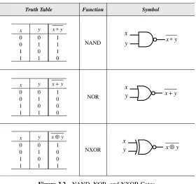
3.5 BASIC LOGIC GATES AND TRUTH TABLES
Logic expressions describe an output as a function of the input and are calledlogic functions. In the digital world, logic gates are used to implement logic functions. There are seven types of logic gates: NOT, AND, OR, NAND, NOR, XOR, and NXOR. These circuit diagrams are symbolic representations of their corresponding logic functions (Figures 3.1 and 3.2).
The logic gates of AND, OR, XOR, NAND, NOR, and NXOR may have more than two inputs. The circuits in Figure 3.3 illustrate multi-input AND and OR logic gates.
3.6 LOGIC REPRESENTATIONS AND CIRCUIT DESIGN
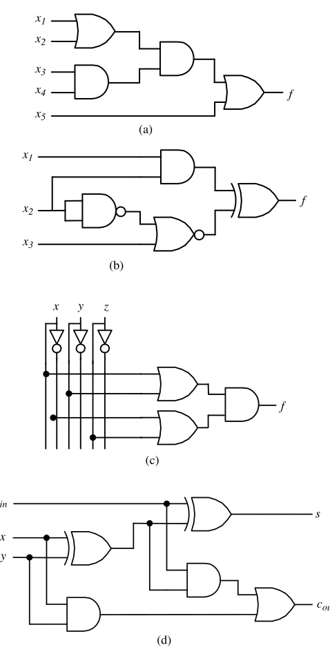
Logic gates are used to represent and implement logic expression into digital circuit diagrams. Consider the following logic function:
fðx;y;zÞ ¼ xyzþxz
The digital circuit (Figure 3.4) implements the function f. The digital circuit consists of elementary logic functions, which are implicit in the logic function. The conversion from logic expressions to circuit diagrams obeys the operator precedence rules shown in Figure 3.5. These precedence rules dictate the order in which the implicit elementary logic functions are implemented.
the input variables through the gates to the output of the circuit. The logic output expression of a gate is determined by the logic expressions at its inputs. Consider the digital circuit shown in Figure 3.6. The logic expression, which represents the logic circuit diagram in Figure 3.6, is expressed as
fðx;y;zÞ ¼ ðxyÞ ðyþzÞ
The XOR function is not listed in Figure 3.5, but since the XOR function is a composite logic function consisting of two AND functions and one OR function, it has the same level of precedence as the AND function.
3.7 TRUTH TABLE
A truth table is generally the first design step. The designer begins with a word statement that describes the function of a digital system. Next, he or she identifies the inputs and outputs of the system and draws a truth table. The inputs and outputs may be single bits or a collection of bits. The truth table consists of input and output
Truth Table Function Symbol
x x
1 0
0 1
NOT
x y x∗y
0 0 0
0 1 0
0 0 1
1 1 1
AND
x y x+y
0 0 0
1 1 0
1 0 1
1 1 1
OR
x y x⊕y
0 0 0
1 1 0
1 0 1
0 1 1
XOR
x
y x y
+ x
y x∗y
x x
x
y x⊕y
Truth Table Function Symbol
x y x∗y
1 0 0
1 1 0
1 0 1
0 1 1
NAND
x y x+y
1 0 0
0 1 0
0 0 1
0 1 1
NOR
x y x⊕y
1 0 0
0 1 0
0 0 1
1 1 1
NXOR
x
y x∗y
x
y x+y
x
y x⊕y
Figure 3.2 NAND, NOR, and NXOR Gates
Figure 3.3 Multi-input AND and OR Logic Gates
x y z
f(x,y,z)
Figure 3.4 Conversion from Logic Function to Circuit Diagram
columns, which characterize the function of the digital circuit. The input columns consist of all possible combinations of inputs. The maximum number of all possible combinations of inputs is 2n, wherenis the number of inputs.
Consider the truth table in Figure 3.7. The digital circuit described by this truth table has three inputs (single bit) and one output (single bit). Since there are three input variables, the maximum combinations of inputs possible is eight. Although one could list the possible combinations of inputs randomly, it is generally strongly recom-mended to use the pattern shown in Figure 3.7. Notice that the right most input column changes every row, the next input column every two rows, and the next input column every four rows. A fourth input column would change every eight rows, and so on. The truth table in Figure 3.7 actually represents Figure 3.4. The process of designing a digital circuit from a truth table is described in Section 3.9.
Order
Precedence Algebra Boolean Algebra
Parentheses Parentheses
First
NOT Exponent
Second
AND Multiplication/division
Third
OR Addition
Last
Figure 3.5 Precedence Rules for Elementary Logic Function Conversion
x y z
f(x,y,z)
Figure 3.6 Conversion from Circuit Diagram to Logic Expression
Row x y z f
1 0
0 0 0
0 1
0 0 1
0 0
1 0 2
0 1
1 0 3
0 0
0 1 4
1 1
0 1 5
0 0
1 1 6
1 1
1 1 7
3.8 TIMING DIAGRAM
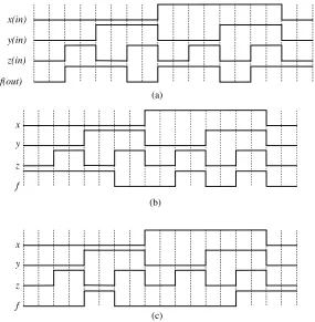
A timing diagram is the graphical representation of input and output signals as functions of time. Since the inputs and outputs can only take the values 0 or 1, their graphical representations are series of square pulses with a variety of time lengths. The inputs and outputs are drawn on the same diagram to show the input–output behavior of the digital system. A timing diagram is usually generated by an oscilloscope or logic analyzer. Computer-aided design tools have software simulator that generate timing diagrams. A timing diagram shows all possible input and output patterns, not necessarily in an order similar to that of a truth table.
Consider the timing diagram in Figure 3.8. Notice that the time intervals are equally separated. Notice also that the output transitions do not occur at exactly the same time that the input transitions occur, but a very short time later. The delay in the output transitions, referred to as the propagation delay, is the time difference between the time of input application and the time when the outputs become valid. The propagation delay is a real physical effect of electronic components that make a logic gate or a circuit. Timing diagrams should show propagation delays. However, during the initial design of a logic circuit, the actual circuit components are not well defined, and therefore any propagation delay can only be estimated. Propagation delays are explored further in Chapter 5.
3.9 LOGIC DESIGN CONCEPTS
If a function is specified in the form of a truth table, an expression that realizes the function can be obtained by considering the rows in the table for which the function is equal to 1 or 0, called thesum-of-productsand theproduct-of-sums,respectively. For a function ofnvariables, a product term in which each of thenvariables appears once is called aminterm. For each row of the truth table, a minterm is formed by the product of the variables (if equal to 1) or their complements (if equal to 0). Similarly, for each row of the truth table, amaxtermis formed by the sum of the variables (if equal to 0) or their complements (if equal to 1). The construction of minterms and maxterms for a logic function is independent of its output. This concept of minterm and maxterm evaluation is illustrated in Figure 3.9, where the rows have been numbered 0 through 7 for reference. All possible combinations of the inputs for a three-variable minterm and maxterms are shown in the figure. The first row, row 0, showsx¼ y¼ z¼ 0 , which
x(input)
y(input)
z(input)
f(output)
Figure 3.8 Timing Diagram
has a corresponding minterm represented by xyzand a corresponding maxterm represented by xþyþz. To further simplify reference to individual minterms and maxterms, they are identified by an index that corresponds to the row numbers. For example, the minterm for row 0 will be referred to asm0, and the maxterm for the same row will be referred to asM0.
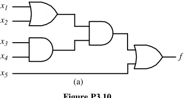
3.10 SUM-OF-PRODUCTS DESIGN
A function can be represented by an expression that is a sum of minterms only, where each minterm is ANDed with every other minterm to represent the function when it is equal to 1. The resulting implementation is functionally correct and unique but not necessarily the lowest-cost realization of the function. The sum of products (SOP) is a logic expression consisting of product (AND) terms that are summed (ORed) with each other. If each product term is a minterm, the expression is called acanonicalsum of products for the function. For example, consider the truth table in Figure 3.10 of a logic functionfof three variables. Using the minterms for which the function is equal to 1, the function can be written explicitly as follows:
fðx;y;zÞ ¼ xyzþxyzþxyzþxyz
Row x y z Minterms Maxterms
0 0 0
0 m0=x⋅y⋅z M x y z
0= + +
1 0 0
1 m1=x⋅y⋅z M1=x+y+z
0 1 0
2 m2=x⋅y⋅z M x y z
2= + +
1 1 0
3 m3=x⋅y⋅z M x y z
3= + +
0 0 1
4 m4 =x⋅y⋅z M4 =x+y+z
1 0 1
5 m5 =x⋅y⋅z M5 =x+y+z
0 1 1
6 m6 =x⋅y⋅z M x y z
6 = + +
1 1 1
7 m7 =x⋅y⋅z M x y z
7 = + +
Figure 3.9 Minterms and Maxterms for Three Variables
Row x y z f
0 0 0 0 0 1 1 0 0 1 0 0 1 0 2 0 1 1 0 3 1 0 0 1 4 1 1 0 1 5 1 0 1 1 6 0 1 1 1 7
Through the use of Boolean algebra identities, this expression can be simplified algebraically as follows:
fðx;y;zÞ ¼ xyzþxyzþxyzþxyz
¼ ðxþxÞ yzþx ðyþyÞ z
¼ 1yzþx1z
¼ yzþxz
This is the minimum-cost sum-of-products expression forf. The cost of a logic circuit is the total number of gates plus the total number of inputs to all gates in the circuit. Minterms, given their row-number subscripts, can be used to specify a given function in a more concise form. The logic function can also be expressed as
fðx;y;zÞ ¼ X
ðm1;m4;m5;m6Þ
or as
fðx;y;zÞ ¼ X
mð1;4;5;6Þ
The symbol Prepresents the logical sum (OR) operation.
3.11 PRODUCT-OF-SUMS DESIGN
Contrary to minterms, which represent the product of variables that set the function to 1, the function can also be represented by the sum of variables, which set the function to 0. Variables used to represent the function using the complement to minterms are calledmaxterms. All possible maxterms for three-variable functions are listed in Figure 3.9. Consider the function specified by a truth table in Figure 3.10; its complement function can be represented by a sum of minterms for which the function is equal to 0. For example, the complement of functionfcan be represented as
fðx;y;zÞ ¼ xyzþxyzþxyzþxyz
¼ m0þm2þm3þm7
Using DeMorgan’s theorem, the functionfcan be represented as
fðx;y;zÞ ¼ m0þm2þm3þm7
¼ m0m2m3m7
¼ M0M2M3M7
¼ ðxþyþzÞ ðxþyþzÞ ðxþyþzÞ ðxþyþzÞ
Using Boolean algebra identities, the function can be reduced:
fðx;y;zÞ ¼ ðxþyþzÞ ðxþyþzÞ ðxþyþzÞ ðxþyþzÞ ¼ ½ðxþzÞ þy ½ðxþzÞ þy ½xþ ðyþzÞ ½xþ ðyþzÞ ¼ ðxþzÞ ðyþzÞ
Using the shorthand method to express the function for the product of sums yields
fðx;y;zÞ ¼ Y
ðM0;M2;M3;M7Þ
¼ YMð0;2;3;7Þ
The symbolQ represents the logical product (AND) operation. More algebraic manipulations and simplifications are explored in the Karnaugh mapping sections in Chapter 6.
3.12 DESIGN EXAMPLES
3.12.1 Multiplexer
Amultiplexeris a combinatorial circuit that has a number (usually, a power of 2) of
data inputs(2n) and nselect inputsused as a binary number to select one of the data inputs. The multiplexer has a single output, which has the same value as the data input selected. Now let us consider a2 : 1 multiplexer. As the name indicates, it has two data inputs,x1andx2, a select input,s,and a single output,y. The output of the circuit will be same as the value of inputx1ifs¼0; otherwise the output will be equal tox2. We can construct a truth table based on these requirements. The truth table of a 2 : 1 multiplexer is shown in Figure 3.11.
From the truth table we can derive the logical expression for the outputy:
yðs;x2;x1Þ ¼ sx2x1þsx2x1þsx2x1þsx2x1
After simplification, the expression is reduced to
yðs;x2;x1Þ ¼ ½sx1 ðx2þx2Þ þ ½sx2 ðx1x1Þ ¼sx1þsx2
s x2 x1 y
0 0 0 0
1 1 0 0
0 0 1 0
1 1 1 0
0 0 0 1
0 1 0 1
1 0 1 1
1 1 1 1
which can be realized using one OR gate and two AND gates. The logic diagram for a 2 : 1 multiplexer is shown in Figure 3.12.
3.12.2 Half-Adder
The half-adder is an example of a simple functional digital circuit built from two logic gates. A half-adder adds two 1-bit binary numbers,xandy. The output is the sum of the two bitssand the carrycout. The truth table for a 1-bit half-adder is shown in Figure 3.13. The logical expressions for the outputs sumsand carrycoutare as follows:
sðx;yÞ ¼ xyþxy¼ xy coutðx;yÞ ¼ xy
These logical expressions can be realized using one XOR gate and one AND gate. The circuit diagram of a 1-bit half-adder is shown in Figure 3.14. The half-adder does not take into account the carry-in from another half-adder. In Chapter 7 we explore full-adder circuits, which can be used to implement the addition of numbers with larger bit sizes.
s x1
x2
y
Figure 3.12 Logic Diagram of a 2 : 1 Multiplexer
x y cout s
0 0
0 0
1 0
1 0
1 0
0 1
0 1
1 1
Figure 3.13 Truth Table of a 1-Bit Half-Adder
x
y s
cout
Figure 3.14 Logic Diagram of a 1-Bit Half-Adder
3.13 NAND AND NOR EQUIVALENT CIRCUIT DESIGN
Through the use of Boolean algebra, it is possible to convert an AND to an OR by inverting the inputs or outputs (DeMorgan’s theorem). The same condition holds true for the logical gates NAND and NOR. Figure 3.15 shows equivalencies for AND and OR. Using DeMorgan’s theorem, one can generate equivalent logic gates for NAND and NOR gates, as shown in Figure 3.16. The circles at the inputs of the AND and OR gates in Figures 3.15 and 3.16 represent inverters. These inverters are referred to as
invert bubbles. Because of the gate equivalency, any logic circuit implemented with NOT, AND, and OR gates could be converted to a logic circuit containing only NAND gates or only NOR gates. This conversion is practical when only one type of gate (NAND or NOR) is available to the designer. In addition, fewer integrated circuits are needed when implementing a logic circuit with NAND or NOR gates.
Often, the final logic circuit is implemented with o