Transport of
Information-Carriers
in Semiconductors and
Nanodevices
Muhammad El-Saba
Ain-Shams University, Egypt
Published in the United States of America by IGI Global
Engineering Science Reference (an imprint of IGI Global) 701 E. Chocolate Avenue
Hershey PA, USA 17033 Tel: 717-533-8845 Fax: 717-533-8661 E-mail: [email protected] Web site: http://www.igi-global.com
Copyright © 2017 by IGI Global. All rights reserved. No part of this publication may be reproduced, stored or distributed in any form or by any means, electronic or mechanical, including photocopying, without written permission from the publisher. Product or company names used in this set are for identification purposes only. Inclusion of the names of the products or companies does not indicate a claim of ownership by IGI Global of the trademark or registered trademark.
Library of Congress Cataloging-in-Publication Data
British Cataloguing in Publication Data
A Cataloguing in Publication record for this book is available from the British Library.
All work contributed to this book is new, previously-unpublished material. The views expressed in this book are those of the authors, but not necessarily of the publisher.
For electronic access to this publication, please contact: [email protected]. Names: El-Saba, Muhammad, 1960- author.
Title: Transport of information-carriers in semiconductors & nanodevices / by Muhammad El-Saba.
Description: Hershey, PA : Engineering SCience Reference, 2017. | Includes bibliographical references.
Identifiers: LCCN 2016057816| ISBN 9781522523123 (hardcover) | ISBN 9781522523130 (ebook)
Subjects: LCSH: Electron transport. | Photon transport theory. | Semiconductors--Transport properties.
Classification: LCC QC611.6.E45 E423 2017 | DDC 621.3815/2--dc23 LC record available at https://lccn.loc. gov/2016057816
Advances in Computer and
Electrical Engineering (ACEE)
Book Series
The fields of computer engineering and electrical engineering encompass a broad range of interdisci-plinary topics allowing for expansive research developments across multiple fields. Research in these areas continues to develop and become increasingly important as computer and electrical systems have become an integral part of everyday life.
The Advances in Computer and Electrical Engineering (ACEE) Book Series aims to publish research on diverse topics pertaining to computer engineering and electrical engineering. ACEE encour-ages scholarly discourse on the latest applications, tools, and methodologies being implemented in the field for the design and development of computer and electrical systems.
Mission
Srikanta Patnaik
SOA University, India
ISSN:2327-039X
EISSN:2327-0403
• Applied Electromagnetics • Algorithms
• VLSI Design • Analog Electronics • VLSI Fabrication • Qualitative Methods • Electrical Power Conversion • Computer Architecture • Programming
• Chip Design
Coverage
IGI Global is currently accepting manuscripts for publication within this series. To submit a pro-posal for a volume in this series, please contact our Acquisition Editors at [email protected] or visit: http://www.igi-global.com/publish/.
Titles in this Series
For a list of additional titles in this series, please visit: www.igi-global.com/book-series
Handbook of Research on Nanoelectronic Sensor Modeling and Applications
Mohammad Taghi Ahmadi (Urmia University, Iran) Razali Ismail (Universiti Teknologi Malaysia, Malaysia) and Sohail Anwar (Penn State University, USA)
Engineering Science Reference • copyright 2017 • 579pp • H/C (ISBN: 9781522507369) • US $245.00 (our price) Field-Programmable Gate Array (FPGA) Technologies for High Performance Instrumentation
Julio Daniel Dondo Gazzano (University of Castilla-La Mancha, Spain) Maria Liz Crespo (International Centre for Theoretical Physics, Italy) Andres Cicuttin (International Centre for Theoretical Physics, Italy) and Fernando Rincon Calle (University of Castilla-La Mancha, Spain)
Engineering Science Reference • copyright 2016 • 306pp • H/C (ISBN: 9781522502999) • US $185.00 (our price) Design and Modeling of Low Power VLSI Systems
Manoj Sharma (BVC, India) Ruchi Gautam (MyResearch Labs, Gr Noida, India) and Mohammad Ayoub Khan (Sharda University, India)
Engineering Science Reference • copyright 2016 • 386pp • H/C (ISBN: 9781522501909) • US $205.00 (our price) Reliability in Power Electronics and Electrical Machines Industrial Applications and Performance Models Shahriyar Kaboli (Sharif University of Technology, Iran) and Hashem Oraee (Sharif University of Technology, Iran) Engineering Science Reference • copyright 2016 • 481pp • H/C (ISBN: 9781466694293) • US $255.00 (our price) Handbook of Research on Emerging Technologies for Electrical Power Planning, Analysis, and Optimization Smita Shandilya (Sagar Institute of Research Technology & Science, India) Shishir Shandilya (Bansal Institute of Research & Technology, India) Tripta Thakur (Maulana Azad National Institute of Technology, India) and Atulya K. Nagar (Liverpool Hope University, UK)
Engineering Science Reference • copyright 2016 • 410pp • H/C (ISBN: 9781466699113) • US $310.00 (our price) Sustaining Power Resources through Energy Optimization and Engineering
Pandian Vasant (Universiti Teknologi PETRONAS, Malaysia) and Nikolai Voropai (Energy Systems Institute SB RAS, Russia)
Engineering Science Reference • copyright 2016 • 494pp • H/C (ISBN: 9781466697553) • US $215.00 (our price) Environmental Impacts on Underground Power Distribution
Osama El-Sayed Gouda (Cairo University, Egypt)
Engineering Science Reference • copyright 2016 • 405pp • H/C (ISBN: 9781466665095) • US $225.00 (our price)
Table of Contents
Preface ... vii Chapter 1
Introduction to Information-Carriers and Transport Models ... 1
Chapter 2
Semiclassical Transport Theory of Charge Carriers, Part I: Microscopic Approaches ... 72
Chapter 3
Semiclassical Transport Theory of Charge Carriers, Part II: Macroscopic Approaches ... 138
Chapter 4
Quantum Transport Theory of Charge Carriers ... 188
Chapter 5
Carrier Transport in Low-Dimensional Semiconductors (LDSs) ... 274
Chapter 6
Carrier Transport in Nanotubes and Nanowires ... 334
Chapter 7
Phonon Transport and Heat Flow ... 379
Chapter 8
Photon Transport ... 450
Chapter 9
Chapter 10
Plasmons, Polarons, and Polaritons Transport ... 587
Chapter 11
Carrier Transport in Organic Semiconductors and Insulators ... 617
Preface
During the last decade, rapid development of electronics has produced new high-speed devices at nanoscale dimensions. These nanodevices have tremendous applications in modern communication systems and computers.
This book, Transport of Information-Carriers in Semiconductors and Nanodevices, is intended to be the first in a series of 3 volumes titled Semiconductor Nanodevices: Physics, Modeling, and Simulation Techniques.
The main purpose of this course is to develop an appreciation and a deep understanding for the con-ceptual foundations underlying the operation of emerging nanoelectronic devices.
I’ve decided to dedicate the first volume to talk about transport modelling, which can serve both academicians and professionals. The next book will cover the Modeling and Simulation Techniques, and will be rather dedicated for professionals and postgraduate students in device simulation. The third book is about Physics and Operation of Modern Nanodevices. However, for the matter of completeness in each book, I squeeze other volumes in a single chapter or as illustrative case studies.
In this book, we study the transport models of information carriers (e.g., electrons and photons) in semiconductors and nanodevices. It contains a comprehensive discussion about carrier transport phe-nomena and includes some topics not previously assembled, altogether, in a single book.
I mean by information carriers, the particles or particle characteristics that carry and transport signals in semiconductor materials and solid-state devices. For instance, the electronic charge in conventional semiconductor devices, the electronic spin in spintronic devices and photons in optoelectronic devices. In fact, the characteristic of any particle may be utilized for information transport. For example, a quan-tum bit (or qubit) of information can be manipulated and encoded in any of several degrees of freedom, notably the photon polarization. In addition, other quasi particles, such as phonons (lattice vibration waves) may be considered as information carriers, because they are capable of transporting thermal energy from point to another in solid-state devices. In fact, some or all of these information carriers may interact in the same device. Indeed, electrons and phonons interact in all semiconductors devices. They also intervene, together with photons in photonic devices, like laser diodes. In the so-called spin light emitting diode (spin LED), the electron spin plays a basic role with all the aforementioned types of information carriers.
Preface
The utilization of TCAD tools is essential because they accelerate the R&D cycle and nowadays, they become essential more than ever. In fact, the device simulation has three main purposes; to understand the underlying physics of a device, to depict the device characteristics and to predict the behavior of new devices. Actually, the advent of new nanodevices has been an everyday occurrence. For example, some versions of the 6th generation of Intel Core processors, is manufactured using a 14nm process. Projecting the advance of semiconductor industry for the next few years, we expect to see nanodevices approaching the size of a few atoms (1nm). The devices at such nanoscale display special quantum properties which are completely different from the case of bulk systems. Therefore, the availability of powerful transport models, which account for the underlying quantum effects, is very important for the simulation of such nanodevices. Everybody working in the field of modeling and simulation of state-of-the-art devices feels that current TCAD tools should be pushed beyond their present limits.
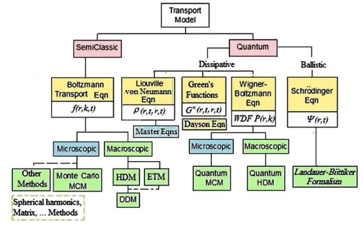
Almost all scientists in the field of semiconductors, agrees that a rigorous study of carrier transport in nanodevices needs a many-body quantum description. Such a description requires the solution of a huge number of equations describing each carrier of the system. Actually, the description of transport in a real device should include the real number of carriers in both the device and its contacts to the external world, and this is beyond the ability of typical computing platforms. Therefore, many levels of approximation that sacrifice some vital information about the physics of transport process are necessary. The figure below illustrates the hierarchy of main transport approaches, which are used in describing carrier transport in semiconductors and nanodevices.
Many authors distinguish between three classes of transport models, namely;
• Quantum models, • Kinetic models, and
• Macroscopic (fluid dynamics) models.
The quantum approach lies at the top level of transport theories, for many-body problems. To treat quantum problems, a mean-field (e.g., the Hartee-Fock potential) approximation is usually adopted to
Preface
transform the many-body system into one-electron problem. The Non-equilibrium Green function (NEGF) method is very popular as a quantum approaches. Above this are quantum kinetic approaches such as the Liouville-von Neumann equation of motion for the density matrix, or Wigner distribution that contain quantum correlations but retain the form of semiclassical approaches. When we move from quantum to classical description of carrier transport, information concerning the phase of the electron and its non-local behavior are lost, and electronic transport is treated in terms of a non-localized particle framework.
The semiclassical transport theory is based on the Boltzmann transport equation (BTE), which rep-resents a kinetic equation describing the time evolution of the distribution function of particle. The BTE has been the primary framework for describing transport in semiconductors and semiconductor devices with micro-scale dimensions. There are then approximations to the BTE, given by moment expansions of the BTE which lead to the hydrodynamic, the drift-diffusion, and relaxation time approximation ap-proaches to transport. Finally, the so-called compact models come at an empirical level as circuit models for circuit simulation.
This book consists of 11 chapters, which are organized as follows.
Chapter 1: Introduction to Information-Carriers and Transport Models
Chapter 2: Semiclassical Transport Theory of Charge Carriers (Part I: Microscopic Approaches) Chapter 3: Semiclassical Transport Theory of Charge Carriers (Part II: Macroscopic Approaches) Chapter 4: Quantum Transport Theory of Charge Carriers
Chapter 5: Carrier Transport in LDS and Nanostructures Chapter 6: Carrier Transport in Nanotubes and Nanowires Chapter 7: Phonon Transport and Heat Flow
Chapter 8: Photon Transport
Chapter 9: Spin Transport and Spintronic Devices
Chapter 10: Polarons, Plasamons, and Polaritons Transport
Chapter 11: Carrier Transport in Organic Semiconductors and Insulators
Preface
I start with the classical approaches and end with the quantum description for composite quasi par-ticles, such as polarons, plasmons, and polaritons.
Each chapter starts with a recap of concerned concepts and provides the state of the art advances in the field as well as some case studies and overview of the literature. Some physical and mathematical notes are inserted (without interrupting the main context) to clarify the jargons, that are unavoidably utilized in such a specialized book.
In Chapter 1, I review the fundamental properties of semiconductors, and explain the transport phe-nomena within the framework of the classical Drudé model. The Drudé classical model is frequently introduced to describe the electrical conductivity in solids. This model is still very relevant because free particle picture can still be used as far as we can assume parabolic energy bands with a suitable effective mass, near equilibrium. In fact, the Drudé model succeeded to explain (to some extent) the electrical conductivity, the thermal conductivity, the Hall Effect, as well as the dielectric function and the optical response of solids. Everything we explain in this chapter about semiconductor properties and carrier transport is correct to the zero order approximation. In order to get into the details of carrier transport in semiconductor devices, we proceed in the following chapters, and search for a master transport equation, in two vertices, namely: the semiclassical and quantum transport theories.
In Chapter 2, I cover the essential aspects of charge carrier transport through solid materials, within the semiclassical transport theory. We start with a review of the semiclassical approaches that leads to the concepts of drift velocity, drift mobility, electrical conductivity and thermal conductivity of charge carriers in metals and semiconductors. The semiclassical transport theory is based on the Boltzmann transport equation (BTE). The Boltzmann transport equation can be derived from the Lowville equation, which describes the evolution of the distribution function changes in phase space and time. I discuss the various approximations and phenomenological approaches which make the equation useful and solv-able for semiconductor devices. For instance, I present the spherical harmonic expansion (SHE) and the Monte Carlo (MC) stochastic Methods as well as the microscopic relaxation-time approximation (RTA), which leads to the conventional drift-diffusion model (DDM).
In Chapter 3, I discuss the hydrodynamic model (HDM) for semiconductor devices, which plays an important role in simulating the behavior of the charge carrier in nano devices. This model consists of a set of nonlinear conservation laws for the particle density, current density, and energy density. The hy-drodynamic model for semiconductors is an inexpensive alternative tool for two- and three-dimensional device simulation. The set of hydrodynamic equations (HDEs), which is derived from the first few mo-ments of the semiclassical BTE, is indeed more accurate than the conventional DDM and less complex than the direct solution of the BTE (by e.g., the SHE and Monte Carlo Methods).
Preface
is called the Wigner-Boltzmann transport function (WBTE). After solving the WBTE, and calculating the Wigner distribution function (WDF), we can calculate the spatial density of carriers and current, as well as the average value of any microscopic physical parameter.
Based on the WBTE, the quantum corrected Boltzmann equation, the quantum hydrodynamic model (QHDM), and the density gradient (DG) approximation can be obtained. Also, the WDF may be defined as the energy integral of the Green’s function. The Green’s function approach can be used to give the response of a system to a constant perturbation in the Schrödinger equation. The so-called non-equilibrium Green’s function (NEGF) formalism is a very powerful technique to evaluate the transport properties of quantum systems in both thermodynamic equilibrium and non-equilibrium conditions. At the end of this chapter, I present the multi-band transport models and the major band structure calcula-tion methods. This includes the ab initio models, such as the density funccalcula-tional theory (DFT), and the approximate methods, such as, the tight binding (TB) model, pseudopotential methods, as well as the GW approximation.
In Chapter 5, I demonstrate the carrier transport phenomena in low-dimensional semiconductors (LDS), where, free electrons are only permitted to move in one or two dimensions. I describe some LDS structures, such as quantum wells, quantum wires and quantum dots and the transport models of charge carriers across them. I discuss the conductance of LDS systems, using the Landauer formalism (for 2-terminal devices) or the generalized Landauer-Büttiker formalism (for multi-terminal devices). I also describe some quantum effects that take place in such nanostructures, such as quantum Coulomb blockade, Aharonov–Bohm, Shubnikov-De Haas oscillations and Kondo effects.
In Chapter 6, I handle transport across Carbon nanotubes (CNT’s), which are one of the most inter-esting materials in nanotechnolog. Nanotubes and nanowires with dimensions on the nanometer length scale cannot be treated as classical conductors because their diameters are as small as the mean free path length (between collisions), but their length is large for the full quantum treatment. Therefore, such mesoscopic structures need a special framework of transport models, which we discuss in this Chapter.
In Chapter 7, I investigate phonon transport and thermal conductivity in semiconductor structures and nanodevices. Microscopic approaches such as the Peierls-Boltzmann transport equation (phonon BTE) and phonon Monte-Carlo simulation can capture quasi-ballistic phonon transport. These models are valid only when heat transport is diffusive and the characteristic length scales are much larger than the phonon mean free path. When phase coherence effects cannot be ignored, these semiclassical ap-proaches fail and result in erroneous results. Therefore, I handle the topic of ballistic (non-diffusive) phonon transport for nanoscale structures and nanodevices.
Preface
The so-called radiative transport equation (RTE) is an integro-differential equation that describe the diffusion and scattering of photons inside matter. The diffusion approximation alleviates the solution of this equation. Also, the optical Bloch equations, which are sometimes called the Maxwell-Bloch equa-tions (MBEs), describe the dynamics of two-state quantum systems interacting with the electromagnetic modes of an optical system. Within a semiclassical approach, where the light field is treated as a classi-cal electromagnetic field and the material excitations are described quantum mechaniclassi-cally, all quantum effects can be treated microscopically on the basis of the semiconductor Bloch equations (SBEs). The quantum approaches are based on some sort of dynamic wave equations (Schrodinger-like or Heisenberg-like) in the microscopic level or the SBEs in the macroscopic level. The so-called dynamics-controlled truncation (DCT) formalism is another successful microscopic approach that describes coherent cor-relations in optically excited semiconductors. On the other hand, the most successful approach to study incoherent effects and correlations in highly excited semiconductors is the nonequilibrium Green’s functions (NEGF) approach. We discuss these models with illustrative examples, to show the features and weakness of each model.
In Chapter 9, I present a full quantum and a semiclassical description of spin transport, which explains how the motion of carriers gives rise to a spin current. The so-called two-component spin-drift-diffusion model (SDDM) is a simple semiclassical and straight-forward method for spin transport modeling. The semiclassical models can be useful for investigation of a broad class of transport problems in semicon-ductors, but they do not include effects of a spin phase memory. The quantum approach of spin density matrix with spin polarization vector of a spin state is more appropriate for this case. The classical Bloch equations for spin transport are the analogue of the classical BTE for particle transport. They can be ex-tended to time-dependent non-equilibrium quantum transport equations, using a suitable non-equilibrium quantum distribution function, like the spin magnetization quantum distribution function (SMQDF). The so-called spinor-BTE resembles the Boltzmann kinetic equation with spin-orbit coupling in a magnetic field together with spin-dependent scattering terms. By taking the macroscopic moments of the spinor-BTE, we can get a density-matrix based version of the SDDM. The last section of this chapter covers the latest proven spintronic devices, such as spin-FET, MRAM and spin LED.
In Chapter 10, I present the semiclassical and full quantum models of composite quasi particles, such as polarons, plasmons and polaritons. These information carriers play a significant role in the emerging nanoelectronic and nanophotonic devices and systems.
In Chapter 11, I focus the attention on the carrier transport in organic semiconductors and insulator materials. Organic semiconductors are hydrocarbon molecular crystals or polymers. In order to under-stand charge transport in organic solids, I review the transport and tunneling mechanisms in disordered materials. Thereupon, I discuss the recent transport models, such as the semiclassical and quantum formalisms of Marcus theory.
Preface
mathematical proofs. In fact, the basic interest of the readers who have an engineering background, is to discover and then to know when and how to apply the different transport models. For these readers I wrote this book. However, when, some mathematical details are important I mention them, in brief, as a note, so that the reader can bypass them without interrupting the main subject.
Although this book is primarily theoretical in approach, I frequently refer to experimental results, which show the variation of transport parameters as well as their measurement methods. I also supple-ment each chapter, with one or two case studies of real devices that aid understanding of the treated theory in this chapter. The book has many illustrations and diagrams to clarify the presented transport models, and comprehensively referenced for further study.
This one-stop book (for almost all semiconductor transport models) is dedicated for engineers and researchers in solid-state physics and nanodevices, as well as students in nanoelectronics and nanotech-nology.
Muhammad El-Saba
1
Chapter 1
DOI: 10.4018/978-1-5225-2312-3.ch001
1. OVERVIEW AND CHAPTER OBJECTIVES
During the last decade, the rapid development of electronics technology has produced several new devices at nanoscale dimensions (nanodevices). Nanodevices, are the tiny devices whose dimensions are in the order of nanometers (or less than 100nm however). The information carriers in these devices are the particles or quasi particles that can carry and transport information objects or signals. The most famous example of an information carrier is the electron charge in conventional semiconductor devices. Also, photons in photonic and optoelectronic devices and the electron spin in spintronic devices can be considered as information carriers. In addition, other quasi particles, such as phonons (quasi par-ticles associated with lattice vibration waves) may be considered as information carriers, because they are capable of transporting energy from point to another in solid-state devices. The recent research in nanodevices is focused around the control of such information carriers and to exploit their features to build new devices with superior characteristics in terms if speed and integration density. Naturally, great efforts have been dedicated to understanding the transport mechanisms of such information carriers in semiconductors and nanostructures.
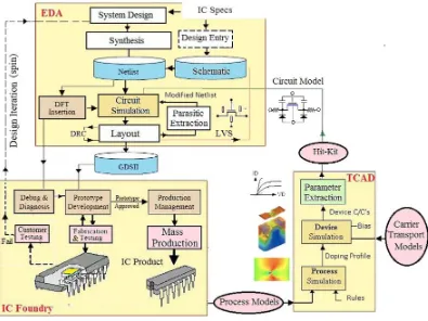
The transport theory of information carriers forms the basis of any physical device model. The transport models are used in Technology/Computer-Aided Design (TCAD) tools to simulate the device behavior, in terms of its structure and geometry as well as external boundary conditions of voltage and current. In fact, the transport of information carriers is a non-equilibrium phenomenon, where the role of external forces plays a crucial role. External forces which drive the device out of equilibrium may be electromagnetic in origin, such as the electric fields associated with an applied bias, or the excitations of electrons by optical sources. Alternately, thermal gradients and electrochemical potentials may also provoke the transport of charge carriers and therefore create external currents and voltages drops, across the device. The Figure1 depicts the role of carrier transport models in TCAD simulation tools and how they are used to calculate the current-voltage (I-V) and capacitance-voltage (C-V) characteristics of a
Introduction to Information-Carriers and Transport Models
certain device and interact with other electronic design automation (EDA) tools. Also, Figure 2 depicts the different levels of transport models, in device simulation. As shown, the TCAD tools are based on semiclassical and quantum transport models. These models range from ab-initio physical models, which
describe the transport of information carriers from first principles down to compact models that describe the outer behavior (usually the I-V and C-V) of devices and circuits. The success of nanotechnology to produce well-functioning nanodevices and systems is mortgaged by the availability of suitable and efficient transport models that meet the challenges at the nanoscale.
As shown in Figure 2, the transport models cover a wide scale, from classical to quantum transport, according to their accuracy and the required computational costs. Actually, a single description in the hierarchy of transport models may not be suitable to provide the correct behavior of all devices.
Depending on the device length scale, the carrier transport may be semiclassical or purely quantum. Nowadays, the most famous semiclassical approaches for the simulation of charge-carrier transport in semiconductor devices are the drift-diffusion model (DDM), the hydrodynamic model (HDM), the Spherical harmonic expansion (SHE) as well as the Monte Carlo method (MCM). DDM and HDM descriptions of particle transport are macroscopic in nature and enable a quick computation of device characteristics (in terms of macroscopic quantities like the carrier density). Depending on the particular application, the macroscopic transport models are applicable to devices with characteristic lengths in
Introduction to Information-Carriers and Transport Models
the range of micrometers or some hundred nanometers, where microscopic-size and quantum effects are not dominant. For even smaller devices, it is necessary to resort to microscopic approaches, which are based on the semiclassical Boltzmann transport equation (BTE) or its quantum counterparts, e.g., the quantum Liouville equation (QBTE) or the Wigner BTE (WBTE).
The solution of the BTE by MCM or SHE approaches may yield accurate results for the transport characteristics in many small devices. However, the semiclassical approaches (both microscopic and macroscopic) fail as soon as quantum mechanical effects dominate and a description of the information carriers as localized particles becomes invalid. Indeed, the description of carrier transport in modern nanodevices requires sophisticated many–body quantum approaches. Clearly, the full quantum description including the actual number of carriers in a device is beyond the ability of any computational platform nowadays1. Therefore, approximations are necessary to simulate and predict the behavior of such devices.
In order to construct a successful approximation (model), we need to understand the phenomena behind the real problem, and under which physical limits, the approximation can be assumed.
Hence, successive levels of approximation, that sacrifice some information about the exact nature of transport, are sometimes utilized in any nanodevices. As shown in Figure 2, the quantum models range from ab-initio models, such as density-functional theory (DFT), and the tight-binding (TB) models that
predict the band structure, to the quantum Liouville equation (QBTE) and its variant master equations as well as the non-equilibrium green functions (NEGF) to predict the device characteristics.
When the appropriate transport model is selected and utilized by a suitable device simulator, we can get the device input/output characteristics and understand the device behavior. Finally, the so-called compact models are non-linear circuit models that capture the device behavior, and are suitable for circuit simulation.
Although we assume a basic knowledge of solid-state physics in this Book, we start with the theoreti-cal fundamentals of semiconductors. This Chapter is a general review of the fundamentals physics of charge carrier transport in semiconductors, with emphasis on the classic transport models.
Upon completion of this chapter, students will
Introduction to Information-Carriers and Transport Models
• Understand the concept of transport modeling and information carriers in semiconductors and
nanodevices.
• Be familiar with the different models of information carrier transport.
• Review the fundamentals of semiconductor physics, such as energy band structure, density of states, drift and diffusion of charge carriers and carrier scattering mechanisms.
• Explain the advantages and disadvantages of the classical transport theory of charge carriers in metals and semiconductors.
• Describe the electrical, thermal, magnetic and optical properties of metals and semiconductors, on the basis of the simple Drudé model.
• Decide what evidence can be used to support or refuse a carrier transport model.
2. CLASSIFICATION OF INFORMATION CARRIERS
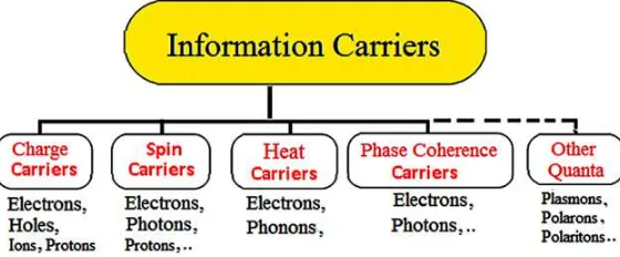
The term Information Carriers has its origin in computer science and information technology and has been applied in many different ways. In computer science, an information carrier is a means to keep (store) information. However, I mean by information carriers in electronic devices, the particles or par-ticle characteristics that can carry, transport or store signals within a device. For instance, the electron charge in conventional semiconductor devices and the spin of electrons in spintronic devices as well as photons in photonic devices are all examples of information carriers. In addition, other quasi particles, such as phonons (quasi particles associated with lattice vibration waves) may be considered as informa-tion carriers, because they are capable of transporting energy from point to another in solid-state devices. Other examples of information carriers are shown in Figure 3.
A charge carrier is a moving particle, which carries an electric charge. Examples are moving electrons, ions and holes. In a conducting medium, an electric field can exert work (force) on the free particles, causing a net motion of their charge through the medium; this is what is referred to as electric current. In metals, the charge carriers are electrons. Free (or more precisely quasi free) electrons in good conduc-tors are able to move about freely within the material. Free electrons can also be generated in vacuum and act as charge carriers. As well as charge, an electron has another intrinsic property, called spin. A spinning charge carrier produces a magnetic field similar to that of a tiny bar magnet.
Introduction to Information-Carriers and Transport Models
In melted ionic solids or electrolytes, such as salt water, the charge carriers are ions, atoms or molecules that have gained or lost electrons so they are electrically charged. Atoms that have gained electrons and become negatively charged are called anions, while atoms that have lost electrons become positively charged and called cations.
In semiconductors, electrons and holes (moving vacancies in the valence band) are the charge carriers. In fact, holes are considered as mobile positive carriers in semiconductors. In semiconductor devices, most of the electrical, thermal and electrical properties of interest have their origins from electrons (in the conduction band) and holes (in the valence band).
Of course electrons and holes carry electrical charges as well energy. Other important energy carri-ers are phonons (lattice vibrations). Actually, the thermal energy transport in crystals occurs primarily due to the vibration of atoms about their equilibrium positions. In semiconductors, the heat conduction process takes place, primarily, through lattice vibrations (phonons).
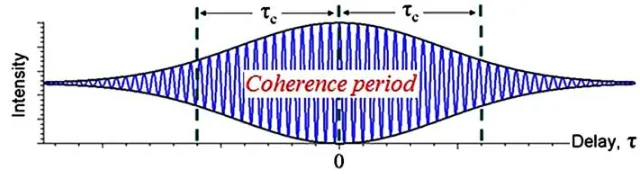
The property of coherence was originally connected with light propagation in optics but now it is defined in all types of waves. In quantum mechanics coherence is due to the nature of the wave functions, which are associated with moving particles. Coherence means that the phase difference between wave functions is kept constant for coherent particles. The delay over which the phase or amplitude wanders by a significant amount is defined as the coherence time (usually termed τc), as shown in Figure 5. The coherence length λc is defined as the distance the wave travels in time τc. The spatial coherence of a wave is defined as the cross-correlation between two points in the wave for all times. The most popular experimental technique which provides direct information about charge carrier coherence in semicon-ductors is four-wave-mixing (FWM) spectroscopy.
Figure 4. Information-carriers in electronics and spintronics
Introduction to Information-Carriers and Transport Models
3. CLASSIFICATION OF TRANSPORT MODELS
The nature of transport in a semiconductor device depends on the characteristic length of the device active region. The carrier motion can be described with classical laws, when the length of the device active region is much larger than the corresponding carrier wavelength. When the device dimensions (or one of them) are comparable to the carrier wavelength, the carriers can no longer be treated as clas-sical point-like particles, and the effects originating from the quantum- nature of propagation begin to determine transport.
The appearance of quantum effects can be determined by comparing the device size2, L, to the
elec-tron mean-free path (λn), or the dephasing length (λϕ) or the de Broglie wavelength (λdB =h/p, where h is
Planck’s constant and p is the electron momentum). The dephasing length (or phase coherence length), λϕ, is a physical quantity which describes the quantum interference and may be defined as follows:
Dephasing length → λϕ = √(Dn τϕ) (1)
where Dn is the electron diffusion constant and τϕ is the dephasing (or phase-breaking) time. One way
to obtain the dephasing time (τϕ,) is to measure the magneto-resistance of the material (Pierret, 2003).
The quantum interference and strong coherence phenomena can be observed in nanostructures, when
λdB≈ L, λn << λϕ (2)
As the temperature is raised, the quantum interference smears out and the coherent states start to appear and participate in conduction. The so-called “weak localization” is expected at the following conditions:
L > λT, λdB≈ λn < λϕ , (3)
where λT is called the temperature length (or thermal correlation length) which is defined as follows:
Temperature length →λT =< ℏ Dn/kBTL (4)
where ℏ=h/2π and kB is Boltzmann’s constant.
On the other hand, the semiclassical approach can be still used in small devices as long as:
λdB << λn, , , λϕ<<L (5)
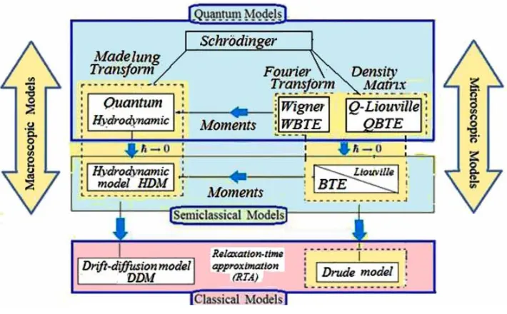
Figure 6 depicts the hierarchy of transport models, which are currently known and utilized to describe electronic transport in semiconductors and nanodevices. At the top level we find the Schrodinger equation3
for many-body problems, which are only tractable for tiny structures with a few numbers of electrons. In order to treat the many-body quantum problem, some sort of mean- approximation is necessary to transform the problem into an effective one-electron problem. This is done in the so-called Hartee-Fock (H-F) equation and other variant methods, such as the Kohn-Sham (K-S) functional approach.
Introduction to Information-Carriers and Transport Models
In semiclassical approaches, we assume that the spatial extent (Δx) of the wave packet, which is as-sociated with the motion of an information carrier, is much smaller than the mean free path between collisions (Δx << λn) in the device area. This means that we can talk about the motion of localized (or
point-like) quasi-particles. Therefore, the main feature size of the device (L) should be much greater than
the mean free length between collisions (L >>λn). The motion should also be localized in the k-space
so that we can talk about a mean wavenumber k>>Δk (satisfying the Heisenberg uncertainty principle Δx.Δk ≈1). This is the level of the Boltzmann transport equation (BTE), which is a kinetic equation
describing the time evolution of the distribution function of particles. The BTE has been the primary framework for describing transport in semiconductors devices down to submicron scale. There are then approximations to the BTE, given by hydrodynamic moments of the BTE which lead to the hydrodynamic model (HDM), the drift-diffusion model (DDM), and relaxation time approximation approaches (RTA).
Figure 8 illustrates the details of transport models of different sophistication levels to describe the transport of charge carriers in semiconductor devices.
Figure 6. Hierarchy of information-carrier transport models
Introduction to Information-Carriers and Transport Models
4. CHARGE-CARRIER TRANSPORT MODELS IN SEMICONDUCTORS
We know that any thermodynamic system is in thermal equilibrium forever unless it is acted upon by
external forces, i.e. when no exchange of energy is done with the exterior. We may consider a semicon-ductor in state of thermal equilibrium, as long as it is not acted upon by any external force field (e.g., electric field, magnetic field, electromagnetic field or light). However, the individual atoms and electrons in a solid still exchange energy between themselves, even when no external force is applied. Therefore, the equilibrium state is called “dynamic thermal equilibrium”.
4.1 Semiconductor Conductivity Model
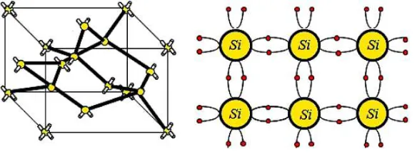
A semiconductor is neither a true conductor nor an insulator, but half way between. The discovery of semiconductor properties, dated back to Michael Faraday (1839) who noticed that the conductivity of some materials decreases as temperature increases, inverse to the behavior of known metals. A variety of substances, such as germanium (Ge), silicon (Si) and gallium arsenide (GaAs), exhibit semiconducting
properties. In this section we first review the model of conduction in semiconductors using the silicon as an example. In fact silicon was established as a good semiconductor material about 80 years ago (the 1930s). At this time, Alan Wilson applied Felix Bloch energy band theory to study the energy band struc-ture of silicon. Actually, the Si atom has 14 electrons distributed over energy levels of different orbitals
(1s2, 2s2, 2p6, 3s2, 3p2). The incomplete outer shell of silicon atom contains 4 electrons (3s2, 3p2). The
silicon lattice has a diamond lattice and its atoms have tetrahedral covalent bonds as shown in Figure 9. In pure silicon lattice all electrons are bound, in the valence band, and there are no free charge car-riers (no free electrons!) at zero absolute temperature (0K). Therefore, behaves like an insulator and the application of an electric field does not result in electric current. In order to produce an electrical
Introduction to Information-Carriers and Transport Models
current in a semi-conductor, some valence electrons must be freed from their bonds. This can be done by supplying the crystal by external energy, usually in the form of heat or light. The minimum energy that is required to free an electron in a pure semiconductor is equal to the height of its energy gap Eg. In
Si, the energy gap is about 1.2eV at 300K. Each free electron in a pure semiconductor leaves a broken bond (or a hole) as shown in Figure 10. Such a free electron roams everywhere in the crystal with equal probability in all directions. A free electron can also recombine with a vacant bond (a hole) to produce a bond, while transmitting its excess energy in the form of light quanta (photons) or lattice vibrations (phonons)
e +hole→bond
←
Recombination
Generation
(6)
If an electric field ζ is applied to a crystal, the free electrons will be acted upon by a force F = -e.ζ
and they begin to drift against the field direction. If the concentration of free electrons in the conduction band is n electrons per unit volume (electrons/cm3) and their average drift velocity is vn, then the electron
current density Jn (A/cm2) is given by:
Jn = - e n vn = σn .ζ (7a)
where σn = - e n (vn / ζ) is called the electrical conductivity of electrons. Unlike metals the conductivity
of semiconductors depends actually on many ambient parameters such as temperature, illumination, etc.
Figure 9. Diamond lattice and covalent bonds in pure elemental semiconductors, like silicon
Introduction to Information-Carriers and Transport Models
Regarding the valence band, it is more convenient to consider the motion of holes instead of the motion
of valence electrons, as shown in Figure 11. This is because the number of holes is usually much less than the number of valence electrons4. If there are p holes (vacant bonds in the crystal lattice) per unit
volume in the valence band, then the current produced by the motion of valence electrons to fill in these holes, against field direction, is equal to the current produced by the motion of holes, along the field direction. Therefore, the hole current density Jp is given by:
Jp = e p vp = σp ζ (7b)
where σp = e p (vp / ζ) is called the electrical conductivity of holes and vp is their average velocity .
Therefore, there exist two types of charge carriers in semiconductors, Electrons in the conduction band, and Holes in the valence band.
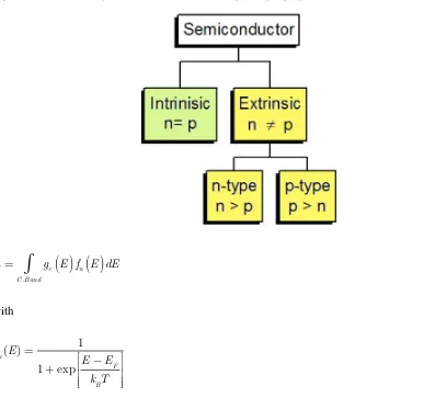
The conduction electrons (and valence holes) in pure semiconductors can be produced by thermal or optical excitations. Extra conduction electrons (or valence holes) can also be obtained in semicon-ductors by doping them with impurity atoms. Accordingly, semiconsemicon-ductors are called intrinsic (pure) semiconductors or extrinsic (impure) semiconductors.
4.2 Concentration of Electrons and Holes
In intrinsic semiconductors, the charge carriers (electrons and holes) are mainly generated by thermal excitation of the valence electrons. When the supplied thermal energy is high enough, some covalent bonds are broken and electron-hole pairs are produced. Therefore, the number of broken bonds and hence the concentration of generated electron-hole pairs is proportional the ambient temperature. Consequently, the concentration of electrons (n) must equal to the concentration of holes (p) in intrinsic semiconductors:
n = p = ni (8)
where ni is called the intrinsic carrier concentration. The intrinsic carrier concentration is temperature
dependent and is given by:
ni = A T3/2 exp (-E
g / 2kBT) (9a)
Introduction to Information-Carriers and Transport Models
where A is a constant. Hence, the value of ni is strongly dependent on temperature and the type of
semi-conductor material. For the matter of comparison, we can express ni by the following relations for Si
and 4H-SiC:
ni (Si) = 3.67x10¹⁶ T3/2 exp (-7020 / T) (9b)
ni (SiC) = 1. 7x10¹⁶ T3/2 exp (-20800 / T) (9c)
In silicon, ni is almost 1.38 x10¹⁰ (electron/cm3) at T= 300 K. On the other hand, n
i is as small as
6.74 x10⁻¹¹ (electron/cm3) or practically zero in SiC at 300 K. For this reason, SiC is more suitable for
high temperature devices.
At thermal equilibrium, the process of electron-hole pair thermal generation is compensated by an opposite electron-hole recombination process, such that the rate of thermal generation gth is equal to
the rate of recombination R. Therefore, the net rate of change of electron-hole pair concentration ∂n/∂t =(gth - R) is null at thermal equilibrium and the intrinsic carrier concentration remains fixed.
In order to increase the number of free charge carriers (electrons or holes) in a semiconductor, and hence to increase its conductivity, semiconductors are usually doped with impurity atoms. In this case the semiconductor is called an extrinsic semiconductor. In extrinsic semiconductors extra conduction electrons are typically produced by doping the semiconductor with impurity atoms of the group V of
the periodic table of elements, like phosphorous (P). This type of impurities is called donors. A
semi-conductor which is doped with donors is said to be of n-type.
Similarly, extra valence holes can be produced by doping the semiconductor with impurity atoms of the group III, like Boron (B). This type of impurities is called acceptors. A semiconductor which is doped with acceptors is said to be of p-type. The more abundant charge carriers in a piece of semiconductor are called majority carriers, which are primarily responsible for current transport. In n-type semiconductors majority carriers are electrons, while in p-type semiconductors they are holes. The less abundant charge carriers are called minority carriers. Minority carriers in n-type semiconductors are holes, while in p-type semiconductors they are electrons.
The density of electrons in the conduction band is equal to the density of occupied states5. Also the
density of occupied states is equal to the density of states in the conduction band gc(E) multiplied by the
probability of occupation which is given by the Fermi-Dirac energy distribution function for electrons
fn(E). Therefore, the density of electrons is given by the following integration:
Introduction to Information-Carriers and Transport Models
The Fermi energy, EF, refers to the energy of the highest occupied energy level at absolute zero
temperature (0K). Also, the density of holes in the valence band is equal to the density of vacant states. The density of vacant states is equal to the density of states in the valence band gv(E) multiplied by the
probability of non-occupation by electrons, which is given by the Fermi-Dirac distribution for holes fp(E)=1-fn(E),
Introduction to Information-Carriers and Transport Models
The density of states g(E) in a certain band can be deduced from the E-k relation of the material,
using the relation.
g E
E k
( )
=( )
∇
∫∫
1 2 3
π
ds
k Const.E.Surface
(14)
Here, the surface integral is taken over a constant energy surface (CES), where E(k) = constant. Figure
14 shows the density of occupied state, which is the product of the density of sates by the Fermi-Dirac distribution function of the concerned carriers. The Figure 15 illustrates this for electrons and holes.
Usually free charge carriers (electrons or holes) reside at the bottom of conduction bands or the top of valence bands. Therefore, we assume that the E(k) relation of the semiconductor is almost
qua-dratic close to extreme points, which concave up conduction bands or concave down valence bands. The approximated E(k) relation is then similar to the dispersion relation of free electrons in free space
(E=p2/2m o=ℏ
2k2/2m
o). However, in order to account for the internal lattice field, the free electron mass
(mo) should be replaced with the carrier effective mass (m*), which depends on the curvature of the
semiconductor E(k) relation. When the semiconductor is anisotropic, the carrier effective mass is a 2nd
order tensor, whose components are given by:
Figure 14. Schematic illustration of the carrier occupation and carrier density
Introduction to Information-Carriers and Transport Models
m E
k k
ij
i j *−1 = 1
2 2 ℏ
∂
∂ ∂ with (i, j = x, y, z) (15)
When the semiconductor is isotropic then the effective mass tensor reduces to a scalar quantity (zero-order tensor), such that: m* = mxx = myy= mzz and other coefficients are null. Therefore, the inverse
effective mass m*-1= (1/ℏ2).∂2E/∂k2.
It comes from the above discussion that the effective mass and so many other characteristics of charge carriers, depend on the band structure E(k), or more precisely, the shape of constant energy surfaces of
the material. In cubic semiconductors, like Si and GaAs, we can distinguish three types of constant energy
surfaces: spherical, ellipsoidal and warped energy bands. Figure 17 shows a general band structure model of cubic semiconductors (near main extreme points). Note that the energy gap may be direct or indirect. The Figure 18 is a schematic of the real band structure, E(k) of Si and GaAs, in certain directions of the
k-space. Also, Figure 19 shows the shape of constant energy surfaces of main conduction and valence bands of such semiconductors. As we’ll see in Chapter 7, the application of strain on a semiconductor shifts the energy levels of the conduction and valence bands and can remove the band degeneracy.
Case 1: Spherical Constant Energy Surfaces
In certain direct-gap semiconductors, like GaAs, the constant energy surfaces of the E-K relation are
almost spherical and isotropic, near extreme points. The E-k relation in this case may be approximated
as follows:
E E
m k k
o o
= ± ℏ
(
−)
2
2
2 * (16a)
Introduction to Information-Carriers and Transport Models
Figure 17. Schematic representation of the band structure of a cubic semiconductor
Figure 18. Energy band structure of Si and GaAs
Introduction to Information-Carriers and Transport Models
where Eo is a constant and the ± sign denotes either the conduction or the valence bands. If the number
of equivalent minima (or valleys) in the conduction band is denoted by Mc, and the effective mass of
electrons is denoted by mn*, then the density of states in the conduction band is given by:
g E M m
Similarly, the density of states in the valence band is given by:
g E M m
Case 2: Ellipsoidal Constant Energy Surfaces
In indirect gap semiconductors, like Si, the constant energy surfaces are ellipsoidal (or approximated
so). The E-k relation is hence a more complicated than the spherical isotropic case. The effective mass
is no longer a scalar quantity but depends on the direction (a tensor). If the directions are chosen such that m* is a diagonalized tensor with diagonal elements mxx*, myy* and mzz*, then, the E-k relation is
Introduction to Information-Carriers and Transport Models
where mnd* is called the density-of-states effective-mass in the conduction band.
mnd* =Mc2 3/
(
m m mxx* yy* zz*)
1 3/ . (19)Case 3: Warped Constant Energy Surfaces
The valence bands of cubic semiconductors (like Si) are approximately quadratic. The constant energy surfaces of the two upper warped bands (for heavy and light holes) are fluted spheres. The E(k) relation
of such semiconductors may be described by the following relations near k= 0,
E k E
where A, B and C are constants and the ± signs correspond to light holes and heavy holes bands,
respec-tively. For the valence band of light holes (with plus sign and designated by the letter l), the effective
mass is usually denoted mlh*. At the band edge, the light holes mass mlh* (for Si) 6 is given by:
Introduction to Information-Carriers and Transport Models
Also, for the valence band of heavy holes (with minus sign and designated by the letter h), the
ef-fective mass is usually denoted mhh*. At the band edge, the heavy hole mass mhh* (for Si) is given by:
mhh* =mo
(
A− B2+1 6 C2)
=0 537. mo (21b)Equation (20), which describes the E(k) relation of the two upper valence bands (the l and h valence
bands) in cubic semiconductors, is sometimes written using polar k-coordinates as follows:
E k E k
m g v
v
( , , )θ ϕ = −ℏ * ( , )θ φ
2 2
2 (22)
where mv* is the isotropic hole effective mass, while g(θ, ϕ) contains the l and h valence bands anisotropy
information. As shown in the following figure, the constant-energy surfaces of l and h hole bands are
warped, like a cube with rounded corners and dented-in faces. This is more pronounced in heavy holes. The third valence band in cubic semiconductors is called the split-off band (s-band). This band is only populated at higher hole energies, and its E(k) relation may be described by the following simple parabolic relation:
E k E k
m A v s
o ( )= −∆ −ℏ
2 2
2 (23)
where Δs is the shift between the top of the s-band and the top of the l and h valence bands. In Si, Δs =0.044
eV below the l and h bands. The effective mass of split-off holes in Si is given by mh,so* = 0.234 mo.
The density of states in the valence band is generally given by:
Introduction to Information-Carriers and Transport Models
where mpd is the density-of-states effective-mass in the valence band:
mpd*3 Mv2 mlh* mhh*3/2 2
=
(
3/2 +)
. (25)where mlh* is the effective mass of light holes and mhh* is the effective mass of heavy holes. For Si, mlh* = 0.16 mo and mhh*=0.49 mo, so that mpd*=0.81mo.
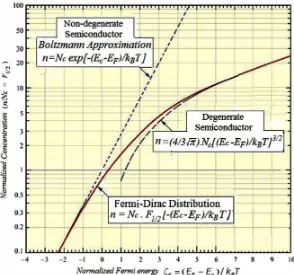
Substituting gc(E) from Equation (18) into (10) yields the following expression for the density of
electrons in the conduction band:
n m
where NC is called the effective density of states in the conduction band:
N m k T
Also F1/2(ζn) is the Fermi-Dirac integral of order ½. The Fermi-Dirac integral is defined as follows7:
F
In non-degenerate semiconductors, where (E-EF) >> kBT, the number of electrons is much smaller
than the effective density of states in conduction band. Then, we have n << Nc (diluted gas of electrons)
Introduction to Information-Carriers and Transport Models
Therefore, the density of electrons may be written as follows:
n N E E k T
c c F B
= −
(
−)
exp (28a)
Similarly, the density of holes in the valence band, in non-degenerates semiconductors, is given by:
p=NV −
(
EF −Ev)
k TB
exp (28b)
where NV is effective density of states in the valence band and given by:
N m k T
some semiconductors at 300K.
In compound semiconductors and alloys, like GaAs, which have upper and lower energy valleys with
different band edges (e.g., Ec1 and Ec2), the density of states in the conduction band maybe expressed
as follows:
It worth notice that equations (28a) and (28b) are not ready for the calculation of the electron and hole concentrations (n, p) because we don’t know yet the Fermi level position (Ec - EF or EF -Ev). In the
Table 1. Effective density of states in conduction and valence bands of some semiconductors at 300K
Semiconductor Eg (eV) mnd / mo mpd / mo Nc (cm-3) N
Introduction to Information-Carriers and Transport Models
following sections we show how to determine the electron and hole concentrations in equilibrium, by an alternative method, from the mass action law and the neutrality condition.
4.3 Mass Action Law in Semiconductors
It follows from the above discussion that the concentration of electrons and holes depends on the loca-tion of Fermi level Ef. In thermal equilibrium, the np product is independent of the Fermi-level position
and given by:
n p Thermal equilibrium n p N N E
k T
o o c v
g
B
. ( )= = exp −
(30)
Here, the subscript ‘o’ denotes the values of n, p at the thermal-equilibrium state.
The above equation is called the mass-action law in semiconductors. According to this law, the n.p
product is equal to a constant independent of time and of the type of added impurities. In intrinsic semi-conductors we have no=po= ni, then the mass-action law can be written as follows:
no po = ni2 (31)
Introduction to Information-Carriers and Transport Models
This means that the n.p product in semiconductor, at thermal equilibrium, is constant equal to the
square of the intrinsic carrier concentration.
4.4 Neutrality Equation in Semiconductors
The electron and hole concentrations as well as the location of the Fermi-energy level in a semicon-ductor can be calculated by the aid of the so-called “neutrality condition”. According to the neutrality
condition, the total charge in a semiconductor at thermal equilibrium is zero. If the charge density (per unit volume) is labeled by ρ then:
- are the densities of ionized donors (bound positive charges) and ionized acceptors
(bound negative charges), respectively. For the calculation of the Fermi-level, each term in the above equation must be expressed in terms of EF. For non-degenerate semiconductors, if the impurity atoms
are localized and singly ionized, then the neutrality equation may be written as follows:
2
where we substituted the ionization ratios for donors and acceptors (Nd+/N
d and Na -/N
a,, respectively)
using Gib’s law8, for singly-ionized impurities (Sze, 1969):
N N
semiconductors). Like most of V-group impurities Ed is close to the bottom of conduction band (44 meV
for P in Si). Such impurities are called shallow-level impurities. Also, Ea is the acceptors energy level
Introduction to Information-Carriers and Transport Models
and heavy holes). For most III-group impurities, Ea is close to the top of valence band (about 10meV),
so that Na- ≈ N
a at room temperature.
The Figure 23 depicts shallow acceptor and donor levels in p-type and n-type semiconductors. Shal-low impurities are of great interest in semiconductors, since they define the conductivity and the type of semiconductor.
The neutrality Equation (33a) can be solved graphically, to find out the Fermi level EF. In special
cases, the analytical solution of this equation may be simple.
4.5 Carrier Density and Fermi Level in Intrinsic Semiconductors
In intrinsic semiconductors, the number of electrons is equal to the number of holes (vacant places or broken bonds). Thus, in thermal equilibrium we have:
no = po = ni (34)
where ni is the intrinsic-carrier concentration in the semiconductor
n np N N E E
Substituting both Nv and Nc expressions into (35) yields the following expression for ni
n m m
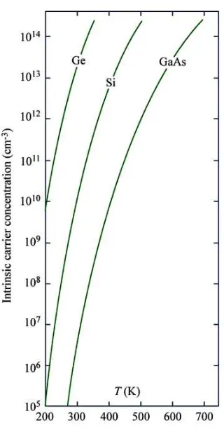
The Figure 24 shows the intrinsic carrier concentration of Si, Ge, and GaAs as a function of
tem-perature. Naturally, the Fermi level in intrinsic materials is almost midway between the conduction and valence band (EF≈ Ei = EV +½ Eg). More precisely, we have:
Introduction to Information-Carriers and Transport Models
Figure 24. Intrinsic carrier concentrations of Si, Ge and GaAs vs. temperature Source: Semiconductors (Smith, 1979).
Introduction to Information-Carriers and Transport Models
Note 1: Meaning of the Fermi Level and Chemical Potential
The Fermi level is the term used to describe the top of the collection of electron energy levels in a solid at absolute zero temperature. At absolute zero temperature (T=0K), electrons pack into the lowest available energy states and build up a Fermi gas, just like a sea of energy states. The Fermi level is the surface of that sea at 0K where no electrons will have enough energy to rise above the surface.
The concept of the Fermi energy is a crucially important concept for understanding the electrical and thermal properties of solids. The Figure 26 shows the Fermi-Dirac energy distribution, f(E), at different
temperatures over the energy band diagram of an intrinsic semiconductor.
According to statistical thermodynamics, the term (μ) that actually appears in the Fermi-Dirac
dis-tribution (f(E)=1/[1+exp-(E-μ)/kBT]), is called the chemical potential of the gas of electrons. However,
the Fermi energy of a free electron gas is related to the chemical potential by the following equation (Kireev, 1979):
Hence, the chemical potential is approximately equal to the Fermi energy at temperatures much less than the characteristic Fermi temperature TF = EF/kB. At room temperature, the Fermi energy and
chemi-cal potential are essentially equivalent.
4.6 Fermi-Level and Carrier Density in Extrinsic Semiconductors
The density of charge carriers (electrons and holes) in an extrinsic semiconductor at thermal equilibrium can be calculated by solving two basic equations, namely, the mass-action law:
nopo =ni2 (37)
Introduction to Information-Carriers and Transport Models
and the neutrality equation:
no +Na− =po +Nd+ (38)
Combining these two equations yields:
n N n
By solving the above two algebraic equation, we get the equilibrium concentrations no and po= ni2/n o
where the ± sign (inside the square brackets) stands for the type of majority carries. That is the + sign is taken when we calculate no from (40a) in n-type materials or po from (40b) in p-type materials. The
minority carriers can be then calculated, simply from the relation po no = ni2.
Case 1: Fermi Level in n-Type Semiconductors
For n-type semiconductors, the electrons are majorities. At moderate temperatures, where all impurities
are ionized (Nd+=N
Therefore, the Fermi level decreases linearly as the temperature is raised. However, at very low temperature, the Fermi level in n-type semiconductors rises initially with temperatures and reaches a maximum and then begins to go down towards the intrinsic level at high temperature. The initial rise of
EF with T is due to the fact that, the donor atoms are not all yet ionized at low temperature. Then, the
Introduction to Information-Carriers and Transport Models
This equation reduces to the following relation at very low temperature, where kBT << (Ec –Ed),
E low temperature E E k T N
Hence, the Fermi level lies at the mid-point between the conduction band edge Ec and the donor level Ed at 0K, and raising the temperature will result in an increase in EF. Substituting this EF into Equation
(26), gives us an expression of electron concentration, n, at very low temperatures.
n N E E
Case 2: Fermi Level in p-Type Semiconductors
Similarly, for p-type semiconductors, holes are majorities. At moderate temperatures, where all acceptors
are ionized (Na- =N
At very low temperature, the fraction of ionized impurities is given by the Gibbs law and the Fermi
level is given by:
This may be approximated as follows:
Introduction to Information-Carriers and Transport Models
Therefore, at T=0, the Fermi level in p-type materials lies midway between the valence band edge Ev and the acceptor level Ea. Substituting this EF into Equation (27), gives us an expression of hole
con-centration, p, at very low temperatures.
p N E E
The Figure 27 depicts the variation of Fermi level in the above three cases with temperature. Also, Figure 28 depicts the variation of electron and hole densities with temperature in n-type and p-type semiconductors.
4.7 Scattering of Charge Carriers
The motion of free charge carriers in a solid (e.g., electrons in a metal or electrons and holes in a semi-conductor) is different from their motion in free space because of collisions with the vibrating nuclei of the solid, as shown in Figure 29. Carriers may also collide with impurity atoms or themselves as well as other crystal defects. These collisions cause the free electrons to scatter in different directions and the resulting motion of electrons is equally probable in all directions (random!) so that there is no net displacement.
Figure 27. Variation of the Fermi level position in semiconductors with temperature