Small Signal Zener Diodes
FEATURES
• Silicon planar power Zener diodes
• Standard Zener voltage tolerance is ± 5 % with
a “B” suffix in the ordering code (e.g.: 1N5221B),
suffix “C” is ± 2 % tolerance
• These diodes are also available in MiniMELF
case with the type designation TZM5221 to
TZM5267, SOT-23 case with the type
designations MMBZ5225 to MMBZ5267 and
SOD-123 case with the types designations MMSZ5225 to
MMSZ5267
• AEC-Q101 qualified
• Material categorization: for definitions of compliance
please see
www.vishay.com/doc?99912
APPLICATIONS
• Voltage stabilization
PRIMARY CHARACTERISTICS
PARAMETER VALUE UNIT
VZ range nom. 2.4 to 75 V
Test current IZT 1.7 to 20 mA
VZ specification Thermal equilibrium
Int. construction Single
ORDERING INFORMATION
DEVICE NAME ORDERING CODE TAPED UNITS PER REEL MINIMUM ORDER QUANTITY 1N5221B to 1N5267B 1N5221B to 1N5267B-series-TR
10 000 per 13" reel
30 000/box 1N5221C to 1N5267C 1N5221C to 1N5267C-series-TR
1N5221B to 1N5267B 1N5221B to 1N5267B-series-TAP 10 000 per ammopack (52 mm tape) 1N5221C to 1N5267C 1N5221C to 1N5267C-series-TAP
PACKAGE
PACKAGE NAME WEIGHT MOLDING COMPOUND
FLAMMABILITY RATING
MOISTURE SENSITIVITY LEVEL
SOLDERING CONDITIONS
DO-35 125 mg UL 94 V-0 MSL level 1
(according J-STD-020) 260 °C/10 s at terminals
ABSOLUTE MAXIMUM RATINGS
(T
amb= 25 °C, unless otherwise specified)
PARAMETER TEST CONDITION SYMBOL VALUE UNIT
Power dissipation TL 25 °C Ptot 500 mW
Zener current IZ Ptot/VZ mA
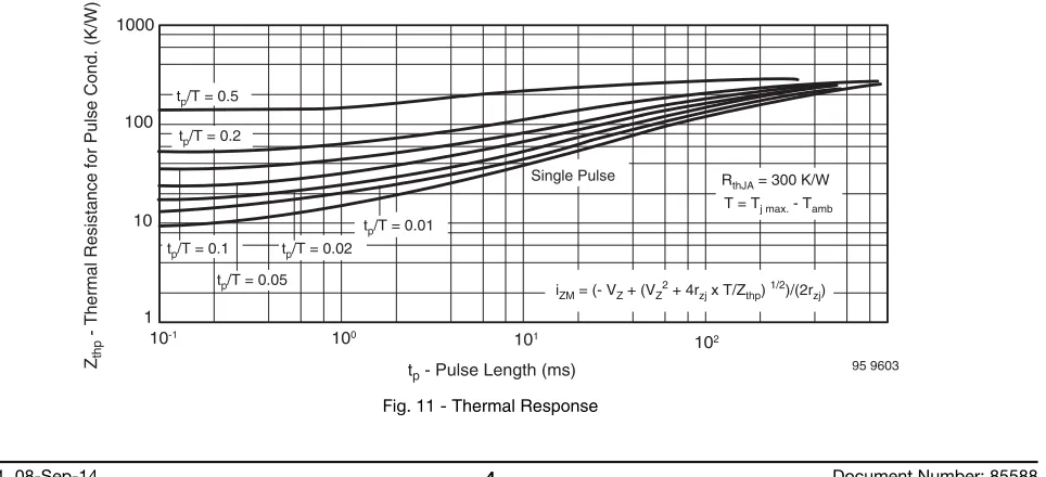
Thermal resistance junction to ambient air I = 4 mm, TL = constant RthJA 300 K/W
Junction temperature Tj 175 °C
Storage temperature range Tstg -65 to +175 °C
Note
(1) Based on DC measurement at thermal equilibrium; lead length = 9.5 (3/8"); thermal resistance of heat sink = 30 K/W
ELECTRICAL CHARACTERISTICS
(T
amb= 25 °C, unless otherwise specified)
PART NUMBER
ZENER VOLTAGE
RANGE (1) TEST CURRENT
REVERSE
NOM. MAX. MAX. MAX. TYP.
1N5221 2.4 20 0.25 100 1 30 1200 - 0.085
1N5261 47 2.7 0.25 0.1 36 105 1000 0.095
1N5262 51 2.5 0.25 0.1 39 125 1100 0.096
1N5263 56 2.2 0.25 0.1 43 150 1300 0.096
1N5264 60 2.1 0.25 0.1 46 170 1400 0.097
1N5265 62 2 0.25 0.1 47 185 1400 0.097
1N5266 68 1.8 0.25 0.1 52 230 1600 0.097
(T
amb= 25 °C, unless otherwise specified)
Fig. 1 - Thermal Resistance vs. Lead Length
Fig. 2 - Typical Change of Working Voltage under Operating Conditions at Tamb= 25 °C
Fig. 3 - Typical Change of Working Voltage vs. Junction Temperature
Fig. 4 - Total Power Dissipation vs. Ambient Temperature
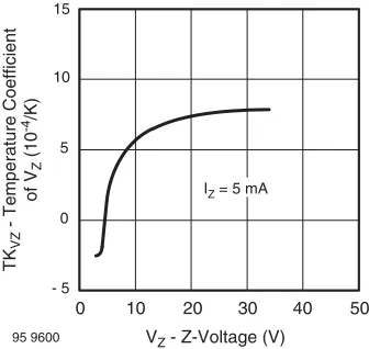
Fig. 5 - Temperature Coefficient of VZ vs. Z-Voltage
Fig. 6 - Diode Capacitance vs. Z-Voltage
95 9611
oltage Change (m
V
- Relative Voltage Change
Tj - Junction Temperature (°C)
240
er Dissipation (m
W
- Diode Capacitance (pF)
Fig. 7 - Forward Current vs. Forward Voltage
Fig. 8 - Z-Current vs. Z-Voltage
Fig. 9 - Z-Current vs. Z-Voltage
Fig. 10 - Differential Z-Resistance vs. Z-Voltage
Fig. 11 - Thermal Response 0 0.2 0.4 0.6 0.8
- Differential Z-Resistance (
Ω
- Thermal Resistance for P
in millimeters (inches):
94 12648
Rev. 1 - Date: 19. December 2011 Document no.: S8-V-3906.04-031(4)
26 min. [1.024] 3.9 max. [0.154] 26 min. [1.024]
Cathode Identification
1.
7
[
0
.0
6
7
]
1
.5 [
0.
059]
3.1 min. [0.120]
Ø
0.
55
m
a
x.
[
0
.022]
Ø
0.
4 m
in.
[
0