The fast growing of technology, specially in communication technology
has help people to get closer and communicate easier one to each other. One of
the most develop in communication system is cellular technology system. SMS as
one of the facility to send a message in cellular technology currently use for SMS
polling system.
In this Final Project, writer will discuss about the assembly process,
design, software of the SMS polling system based on ATMega 16, MMC as data
storage, and seven segment as visual media. Microcontroller ATMega 16 as one
of the processor will act as a “brain” in this SMS polling system. With the simple
and small form, and with it fast ability to process the system, it expected to create
some simple, portable, and useful SMS polling system. The price of
microcontroller that less than personal computer also expected to reduce the cost
of the polling system.
ABSTRAK
Perkembangan teknologi yang semakin pesat, khususnya di bidang
teknologi komunikasi memudahkan orangorang untuk berkomunikasi satu dan
yang lain. Salah satu teknologi komunikasi yang berkembang sangat pesat adalah
teknologi selular. SMS sebagai salah satu fasilitas berkirim pesan dalam teknologi
selular sering kali digunakan sebagai fasilitas untuk melakukan poling SMS.
Dalam Tugas Akhir kali ini akan dibahas mengenai perancangan, desain
dan pemrograman sistem poling SMS berbasis mikrokontroler ATMega 16 dan
MMC sebagai penyimpan data, serta sebagai media visual digunakan
seven
segment
untuk menampilkan hasil poling SMS. Mikrokontroler ATMega 16
sebagai salah satu prosesor berperan sebagai ”otak” dalam sistem poling SMS,
ukuran yang kecil dan sederhana serta kemampuan dalam memproses diharapkan
dapat menciptakan suatu sistem poling yang sederhana,
portabel
, dan mudah
untuk digunakan. Harganya yang relatif lebih murah dari PC pun dapat menekan
harga dari sistem poling tersebut.
LEMBAR PENGESAHAN
SURAT PERNYATAAN
ABSTRAK
i
ABSTRACT
ii
KATA PENGANTAR
iii
DAFTAR ISI
v
DAFTAR TABEL
viii
DAFTAR GAMBAR
ix
BAB I PENDAHULUAN
1
I.1. Latar Belakang
1
I.2. Identifikasi Masalah
1
I.3. Tujuan
1
I.4. Pembatasan Masalah
2
I.5. Spesifikasi Alat
2
I.6. Metodologi
2
I.7. Sistematika Penulisan
2
BAB II DASAR TEORI
4
II.3.2. Format PDU
16
II.4.
Software
pendukung
17
II.4.1. AVR Studio 4
17
II.4.2. PonyProg2000 V1.5
18
BAB III PERANCANGAN DAN REALISASI
19
III.1. Diagram Blok dan Cara Kerja
19
III.2. Perancangan
Hardware
20
III.2.1. Mikrokontroler ATMega 16
20
III.2.2.
Interface
ATMega 16 ke HP Siemens C35i
22
III.2.3.
Interface
ATMega 16 ke MMC
23
III.3.4.
Interface
ATMega 16 ke
Seven Segment
23
III.3. Perancangan
Software
24
BAB IV DATA PENGAMATAN DAN ANALISA
28
IV.1. Data PDU SMS
28
IV.2. Analisa Percobaan
29
BAB V KESIMPULAN DAN SARAN
32
V.1. Kesimpulan
32
V.2. Saran
32
DAFTAR PUSTAKA
33
LAMPIRAN A
FOTO ALAT
A1
LAMPIRAN B
BAHASA ASSEMBLY
B1
Tabel II.1. Fungsi dan Karakteristik pinpin pada MMC
13
Tabel II.2. Beberapa perintah
command
MMC yang biasa digunakan
14
Tabel II.3. Format PDU terima
16
Tabel II.4. Format PDU kirim
17
Tabel III.1. Pinpin mikrokontroler yang digunakan
21
Tabel III.2. Nilai register untuk mode operasi 19200 bps
22
Tabel III.3. Hubungan Port C ke
seven segment
24
Tabel IV.1. Data nomer
user
28
DAFTAR GAMBAR
Gambar II.1. Arsitektur ATMega 16
5
Gambar II.2. Konfigurasi pin ATMega 16
6
Gambar II.3. Konfgurasi Memori Data ATMega 16
8
Gambar II.4. Perubahan shift register saat komunikasi SPI
12
Gambar II.5. Gambar posisi pinpin pada MMC
14
Gambar III.1. Diagram Blok Sistem
19
Gambar III.2. Desain skematik sistem
21
Gambar III.3. Pinpin pada seven segment
23
Gambar III.4. Diagram alir program utama
25
Gambar III.5. Diagram alir kirim perintah ke ponsel
26
Gambar III.6. Diagram alir kirim data PDU ke ponsel
26
Gambar III.7. Diagram alir inisialisasi MMC
27
Gambar III.8. Diagram alir simpan dan ambil data ke MMC
27
Gambar IV.1. Contoh SMS “POLLING” dan SMS pertanyaan
30
Gambar IV.2. Contoh SMS jawaban dan SMS respon penutup
30
.def data = r23 .def teg = r24 .def tmmcbyte = r21 .def rmmcbyte = r22 .equ a = 0b01000001 .equ b = 0b00110001 .equ c = 0b01110011 .equ satu = 0b11101101 .equ dua = 0b01000011 .equ tiga = 0b01001001 .equ empat = 0b00101101 .equ lima = 0b00011001 .equ enam = 0b00010001 .equ tujuh = 0b11001101 .equ lapan = 0b00000001 .equ bilan = 0b00001001 .equ nol = 0b10000001
.org 0x0000 rjmp main
main:
ldi r16, low(ramend) out spl, r16
ldi r16, high(ramend) out sph, r16
ldi r16,0xFF out ddra, r16 out ddrc,r16
clear:
ldi r16, 0x00 ldi r23, 0x00 ldi Xl, low(0x0200) ldi Xh, high(0x0200) clir:
st X+, r16 inc r23
cpi r23,0x8F breq main2 rcall clir
main2:
tunggu_SMS: rcall usart_rx cpi rxbyte,$31 breq read
rjmp tunggu_SMS
read:
rcall kirim_CMGR
skip_cmgr1: rcall usart_rx cpi rxbyte,$30 breq skip_cmgr2 rjmp skip_cmgr1 skip_cmgr2: rcall usart_rx cpi rxbyte,$30 breq Simpan_1 rjmp skip_cmgr2
simpan_1:
ldi r16,0
ldi Xl, low(SRAM) ldi Xh, high(SRAM) simpan1:
rcall usart_rx st X+, rxbyte cpi r16,0x40 breq pisahkannomer inc r16
rjmp simpan1
pisahkannomer: ldi r16, 0x00 ldi Xl, low(0x0100) ldi Xh, high(0x0100) ldi Yl, low(0x0071) ldi Yh, high(0x0071) pisah:
ld r19, Y+ st X+, r19 cpi r16, 0x0F breq simpannommc1 inc r16
brne cek_nomer cpi r16, 0x05 breq kirimtanya inc zl
inc r16 rjmp loopcek kirimtanya:
rjmp kirimtanya1
cek_nomer: ldi r16, 0x00 ldi Xl, low(0x0100) ldi Xh, high(0x0100) ldi Yl, low(0x0071) ldi Yh, high(0x0071) ceknomer:
ld r19, Y+ ld r20, X+ cp r20, r19 brne tunggu cpi r16, 0x0F breq ceknotanya inc r16
rcall ceknomer tunggu:
rjmp tunggu_SMS
ceknotanya:
ldi Xl, low(0x009E) ldi Xh, high(0x009E) loopcekjwb1: ld r16,X cpi r16,$43 breq jwbtanya1 cpi r16,$34 breq jwbtanya2 rjmp tunggu_SMS
;=================== ;jawaban pertanyaan 1 ;=================== jwbtanya1:
jawaban_1A:
ldi Xl, low(0x0200) ldi Xh, high(0x0200) ld r16, X
inc r16 st X, r16 rcall kirimtanya2 rjmp tunggu_SMS jawaban_1B:
ldi Xl, low(0x0202) ldi Xh, high(0x0202) ld r16, X
inc r16 st X, r16 rcall kirimtanya2 rjmp tunggu_SMS jawaban_1C:
ldi Xl, low(0x0204) ldi Xh, high(0x0204) ld r16, X
inc r16 st X, r16 rcall kirimtanya2 rjmp tunggu_SMS
;==================== ;jawaban pertanyaan 2 ;==================== jwbtanya2:
ldi Xl, low(0x0200) ldi Xh, high(0x0200) ld r16,X cpi r16,$35 breq jawaban_2A cpi r16,$39 breq jawaban_2B cpi r16,$44 breq jawaban_2C rjmp tunggu_SMS
jawaban_2A:
ldi Xl, low(0x0206) ldi Xh, high(0x0206) ld r16, X
ld r16, X inc r16 st X, r16 rcall kirimmakasih rjmp tunggu_SMS
;=================== ;kirim pertanyaan 1 ;=================== kirimtanya1:
ldi Xl, low(0x020C) ldi Xh, high(0x020C) ld r16, X
cpi r16,0x01 breq tunggu_SMS1 inc r16
st X, r16 tunggu_SMS1: rjmp tunggu_SMS
rcall timer1d simpannommc: rcall cmd24 rcall tulis
rcall kirim_cmgs
tunggu1: rcall usart_rx cpi rxbyte,$3E breq kirimheadanno1 rjmp tunggu1
kirimheadanno1: rcall kirimheader
kirim_pertanyaan:
ldi zl, low(2*datapertanyaan1) ldi zh, high(2*datapertanyaan1) loop_kirimpertanyaan:
lpm
mov txbyte,r0 cpi txbyte,0 breq cntrlZ1 rcall usart_tx inc zl
;================= ;kirim pertanyaan 2 ;================= kirimtanya2:
rcall timer1d rcall kirim_cmgs
tunggu2: rcall usart_rx cpi rxbyte,$3E breq kirimheadanno2 rjmp tunggu2
kirimheadanno2: rcall kirimheader
kirim_tanya2:
ldi zl, low(2*datapertanyaan2) ldi zh, high(2*datapertanyaan2) loop_kirimatanya2:
lpm
mov txbyte,r0 cpi txbyte,0 breq cntrlZ2 rcall usart_tx inc zl
rjmp loop_kirimatanya2 cntrlZ2:
rcall cntrl_z inc r25
rcall tampildata1 rjmp tunggu_SMS
;================= ;kirim terimakasih ;================= kirimmakasih:
ldi Xl, low(0x020C) ldi Xh, high(0x020C) ld r16, X
dec r16 st X, r16 rcall timer1d rcall kirim_cmgs
cpi txbyte,0 breq cntrlZ3 rcall usart_tx inc zl
rjmp loop_kirimakasih cntrlZ3:
rcall cntrl_z rcall tampildata2 rjmp tunggu_SMS
;======================= ;kirim header dan nomer
;======================= kirimheader:
rcall timer1d
ldi zl, low(2*headerkirim) ldi zh, high(2*headerkirim) loop_header:
lpm
mov txbyte,r0 cpi txbyte,0 breq kirim_nomer rcall usart_tx inc zl
rjmp loop_header
kirim_nomer: rcall cmd17 rcall baca ldi r16, 0x00 ldi Xl, low(0x0100) ldi Xh, high(0x0100) loop_kirimnomer:
ld txbyte, X+ rcall usart_tx cpi r16,0x0F breq endheadno inc r16
rjmp loop_kirimnomer endheadno:
ret
cpi txbyte,0 breq tunggueror rcall usart_tx inc zl
rjmp load_CNMI tunggueror:
rcall usart_rx cpi rxbyte,$52 breq endcnmi rjmp tunggueror endcnmi:
ret
;============= ;kirim at+cmgd ;============= kirim_cmgd: rcall timer1d rcall timer1d rcall timer1d
ldi zl, low(2*cmgd) ldi zh, high(2*cmgd) loop_cmgd:
lpm
mov txbyte,r0 cpi txbyte,0 breq tunggu_ok rcall usart_tx inc zl
rjmp loop_cmgd tunggu_ok:
rcall usart_rx cpi rxbyte,$4B breq enddel rjmp tunggu_ok enddel:
ret
;=============== ;kirim at+cmgr=1 ;=============== kirim_CMGR:
ldi zl, low(2*CMGR) ldi zh, high(2*CMGR) load_CMGR:
lpm
ldi zl, low(2*cmgs) ldi zh, high(2*cmgs) loop_cmgs:
lpm
mov txbyte,r0 cpi txbyte,0 breq endcmgs rcall usart_tx inc zl
rjmp loop_cmgs endcmgs:
ret
;============= ;kirim cntrl Z ;============= cntrl_Z:
ldi txbyte,$1A rcall usart_tx tungguok: rcall usart_rx cpi rxbyte,$4B breq endz rjmp tungguok endz:
ret
tampildata1: ldi r19,0x0F rcall data1a ldi r16,0xff out portc,r16 rcall timer1d ldi r19,0x0F rcall data1b ldi r16,0xff out portc,r16 rcall timer1d ldi r19,0x0F rcall data1c ldi r16,0xff out portc,r16 rcall timer1d ret
rcall data2b ldi r16,0xff out portc,r16 rcall timer1d ldi r19,0x0F rcall data2c ldi r16,0xff out portc,r16 rcall timer1d ret
;======================= ;tampilkan data poling 1
;======================= data1a:
dec r19 cpi r19,0x00 breq return1a ldi r20,0xFF loop1a:
dec r20
ldi Xl, low(0x0200) ldi Xh, high(0x0200) ld r16, X
ldi teg,0x10 ldi data,satu rcall display ldi teg,0x08 ldi data,a rcall display ldi teg, 0x04 ldi data, nol rcall display ldi teg, 0x02 ldi data, nol rcall display rcall banding00x cpi r20,0x00 breq data1a rjmp loop1a return1a: ret
data1b: dec r19 cpi r19,0x00 breq return1b ldi r20,0xFF loop1b:
rcall display ldi teg, 0x02 ldi data, nol rcall display rcall banding00x cpi r20,0x00 breq data1b rjmp loop1b return1b: ret
data1c: dec r19 cpi r19,0x00 breq return1c ldi r20,0xFF loop1c:
dec r20
ldi Xl, low(0x0204) ldi Xh, high(0x0204) ld r16, X
ldi teg,0x10 ldi data,satu rcall display ldi teg,0x08 ldi data,c rcall display ldi teg, 0x04 ldi data, nol rcall display ldi teg, 0x02 ldi data, nol rcall display rcall banding00x cpi r20,0x00 breq data1c rjmp loop1c return1c: ret
;======================= ;tampilkan data poling
;======================= data2a:
ldi data,dua rcall display ldi teg,0x08 ldi data,a rcall display ldi teg, 0x04 ldi data, nol rcall display ldi teg, 0x02 ldi data, nol rcall display rcall banding00x cpi r20,0x00 breq data2a rjmp loop2a return2a: ret
data2b: dec r19 cpi r19,0x00 breq return2b ldi r20,0xFF loop2b:
dec r20
ldi Xl, low(0x0208) ldi Xh, high(0x0208) ld r16, X
ldi teg,0x10 ldi data,dua rcall display ldi teg,0x08 ldi data,b rcall display ldi teg, 0x04 ldi data, nol rcall display ldi teg, 0x02 ldi data, nol rcall display rcall banding00x cpi r20,0x00 breq data2b rjmp loop2b return2b: ret
rcall display ldi teg, 0x04 ldi data, nol rcall display ldi teg, 0x02 ldi data, nol rcall display rcall banding00x cpi r20,0x00 breq data2c rjmp loop2c return2c: ret
;================ ;bandingkan hasil ;================ banding00x:
display:
out PORTA,teg out PORTC,data rcall timer ret
;================ ;inisialisasi SPI ;================ spi_init:
cbi PortB,6 sbi PortB,5 sbi PortB,7 sbi PortB,4
ldi r16, 0b01010011 out spcr,r16
cbi PortB,4 ret
;=========== ;kirim CMD0 ;=========== cmd0:
ldi tmmcbyte,0xFF rcall transmmc ldi tmmcbyte,0x40 rcall transmmc ldi tmmcbyte,0x00 rcall transmmc rcall transmmc ldi tmmcbyte,0x95 rcall transmmc cpi rmmcbyte,0x01 breq kembalimmc1 rjmp cmd0
kembalimmc1: ret
;=========== ;kirim CMD24 ;=========== cmd24:
ldi tmmcbyte,0xFF rcall transmmc ldi tmmcbyte,0x58 rcall transmmc mov tmmcbyte,r25 rcall transmmc
;=========== cmd17:
ldi tmmcbyte,0xFF rcall transmmc ldi tmmcbyte,0x51 rcall transmmc mov tmmcbyte,r25 rcall transmmc
di tmmcbyte, high(0x200) rcall transmmc
ldi tmmcbyte, low(0x200) rcall transmmc
ldi tmmcbyte,0xFF rcall transmmc cpi rmmcbyte,0x01 breq kembalimmc3 rjmp cmd17
kembalimmc3: ret
;============ ;MMC initial ;============ mmc_init: sbi portb,4 ldi r16, 0 dummy: inc r16
ldi tmmcbyte,0xFF rcall transmmc cpi r16,80 brne dummy rcall cmd0 ret
transmmc:
out spdr,tmmcbyte sbis spsr,spif rjmp transmmc in rmmcbyte,spdr ret
;========== ;tulis mmc ;========== tulis:
rcall transmmc loopwrite:
ld tmmcbyte,X+ rcall transmmc inc r16 cpi r16,0x0F brne loopwrite ldi tmmcbyte,0xFF rcall transmmc rcall transmmc mov r16,rmmcbyte andi r16,0x1F cpi r16,0x05 breq tulis ret
;========= ;baca mmc ;========= baca:
ldi tmmcbyte, 0xFF rcall transmmc cpi rmmcbyte, 0xFE brne baca
ldi xl,low(0x100) ldi xh,high(0x100) ldi r16,0
loopbaca: sbis ucsra,udre rjmp loopbaca ldi tmmcbyte, 0xFF rcall transmmc st x+,rmmcbyte inc r16 cpi r16,0x0F breq slesaibaca rjmp loopbaca slesaibaca: ldi tmmcbyte,0xFF rcall transmmc rcall transmmc ret
;================== ;inisialisasi USART ;================== init_usart:
sbis UCSRA,UDRE rjmp usart_tx out UDR,txbyte ret
;============ ;receive data ;============ usart_rx:
sbis UCSRA,RXC rjmp usart_rx in rxbyte, UDR ret
;====== ;Timer ;====== timer1d:
ldi r16, 0b00000100 out TIMSK, r16 ldi r16, high(0xD5D0) out TCNT1H, r16 ldi r16, low(0xD5D0) out TCNT1L, r16 ldi r16, 0b00000101 out TCCR1B, r16 looptimer:
in r19, TIFR sbrs r19, TOV1 rjmp looptimer
ldi r16, 0b00000100 out TIFR, r16 ret
timer:
ldi r16, 0b00000100 out TIMSK, r16 ldi r16, high(0xFFFF) out TCNT1H, r16 ldi r16, low(0xFFFF) out TCNT1L, r16 ldi r16, 0b00000101 out TCCR1B, r16 looptimer2:
datasms:
.db "07D0279399741E01",0 ;POLLING headerkirim:
.db "07912618485400F91100",0 datapertanyaan1:
.db
"00000047D3F49C5E6E83E065F93DCC4E87DDA069900A0AAFC36E90B82C5787D9613748 1C4EAF5DA0A06B5EA6D7D57590D0250F9FEBA0A18B9E2687D7A079995E57D701",0
datapertanyaan2: .db
"00000047D32015D42EB7C565797A1D7683E66F767D9E0691C3EC701B042FCBEF61763AE C76814041D7BC4CAFABEB20A14B1E3ED74143173D4D0EAF41F332BDAEAE8300",0
makasih: .db
"00000048D4B23CDD0EAFC3F3341A14A687E72078584E4FCFD3F0F03C0D0ABBC96117881CA687 416137390C0AAFC36ED0BC7C2ECBC320721A2E7FCFCB7317284C6EA7DD",0
CNMI:
.db "at+cnmi=1,1,0,1,1",13,10,0 CMGR:
.db "at+cmgr=1",13,10,0 cmgs:
.db "at+cmgs=77",13,10,0 cmgd:
– 32 x 8 General Purpose Working Registers – Fully Static Operation
– Up to 16 MIPS Throughput at 16 MHz – On-chip 2-cycle Multiplier
• Nonvolatile Program and Data Memories
– 16K Bytes of In-System Self-Programmable Flash Endurance: 10,000 Write/Erase Cycles
– Optional Boot Code Section with Independent Lock Bits In-System Programming by On-chip Boot Program True Read-While-Write Operation
– 512 Bytes EEPROM
Endurance: 100,000 Write/Erase Cycles – 1K Byte Internal SRAM
– Programming Lock for Software Security
• JTAG (IEEE std. 1149.1 Compliant) Interface
– Boundary-scan Capabilities According to the JTAG Standard – Extensive On-chip Debug Support
– Programming of Flash, EEPROM, Fuses, and Lock Bits through the JTAG Interface
• Peripheral Features
– Two 8-bit Timer/Counters with Separate Prescalers and Compare Modes – One 16-bit Timer/Counter with Separate Prescaler, Compare Mode, and Capture
Mode
– Real Time Counter with Separate Oscillator – Four PWM Channels
– 8-channel, 10-bit ADC 8 Single-ended Channels
7 Differential Channels in TQFP Package Only
2 Differential Channels with Programmable Gain at 1x, 10x, or 200x – Byte-oriented Two-wire Serial Interface
– Programmable Serial USART – Master/Slave SPI Serial Interface
– Programmable Watchdog Timer with Separate On-chip Oscillator – On-chip Analog Comparator
• Special Microcontroller Features
– Power-on Reset and Programmable Brown-out Detection – Internal Calibrated RC Oscillator
– External and Internal Interrupt Sources
– Six Sleep Modes: Idle, ADC Noise Reduction, Power-save, Power-down, Standby and Extended Standby
• I/O and Packages
– 32 Programmable I/O Lines
– 40-pin PDIP, 44-lead TQFP, and 44-pad MLF
• Operating Voltages
– 2.7 - 5.5V for ATmega16L – 4.5 - 5.5V for ATmega16
• Speed Grades
– 0 - 8 MHz for ATmega16L – 0 - 16 MHz for ATmega16
8-bit
Microcontroller
with 16K Bytes
In-System
Programmable
Flash
ATmega16
ATmega16L
Pin Configurations
Figure 1. Pinouts ATmega16(XCK/T0) PB0 (T1) PB1 (INT2/AIN0) PB2 (OC0/AIN1) PB3 (SS) PB4 (MOSI) PB5 (MISO) PB6 (SCK) PB7 RESET VCC GND XTAL2 XTAL1 (RXD) PD0 (TXD) PD1 (INT0) PD2 (INT1) PD3 (OC1B) PD4 (OC1A) PD5 (ICP) PD6
PA0 (ADC0) PA1 (ADC1) PA2 (ADC2) PA3 (ADC3) PA4 (ADC4) PA5 (ADC5) PA6 (ADC6) PA7 (ADC7) AREF GND AVCC PC7 (TOSC2) PC6 (TOSC1) PC5 (TDI) PC4 (TDO) PC3 (TMS) PC2 (TCK) PC1 (SDA) PC0 (SCL) PD7 (OC2)
PA4 (ADC4) PA5 (ADC5) PA6 (ADC6) PA7 (ADC7) AREF GND AVCC PC7 (TOSC2) PC6 (TOSC1) PC5 (TDI) PC4 (TDO) (MOSI) PB5
(MISO) PB6 (SCK) PB7 RESET VCC GND XTAL2 XTAL1 (RXD) PD0 (TXD) PD1 (INT0) PD2
Overview
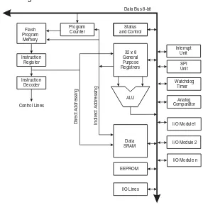
The ATmega16 is a low-power CMOS 8-bit microcontroller based on the AVR enhanced RISC architecture. By executing powerful instructions in a single clock cycle, the ATmega16 achieves throughputs approaching 1 MIPS per MHz allowing the system designer to optimize power consumption versus processing speed.Block Diagram
Figure 2. Block DiagramINTERNAL OSCILLATOR OSCILLATOR WATCHDOG TIMER MCU CTRL. & TIMING OSCILLATOR TIMERS/ COUNTERS INTERRUPT UNIT STACK POINTER EEPROM SRAM STATUS REGISTER USART PROGRAM COUNTER PROGRAM FLASH INSTRUCTION REGISTER INSTRUCTION DECODER PROGRAMMING LOGIC SPI ADC INTERFACE COMP. INTERFACE PORTA DRIVERS/BUFFERS
PORTA DIGITAL INTERFACE
GENERAL PURPOSE REGISTERS X Y Z ALU + -PORTC DRIVERS/BUFFERS
PORTC DIGITAL INTERFACE
PORTB DIGITAL INTERFACE
PORTB DRIVERS/BUFFERS
PORTD DIGITAL INTERFACE
PORTD DRIVERS/BUFFERS XTAL1 XTAL2 RESET CONTROL LINES VCC GND MUX & ADC AREF
PA0 - PA7 PC0 - PC7
The AVR core combines a rich instruction set with 32 general purpose working registers. All the 32 registers are directly connected to the Arithmetic Logic Unit (ALU), allowing two independent registers to be accessed in one single instruction executed in one clock cycle. The resulting architecture is more code efficient while achieving throughputs up to ten times faster than conventional CISC microcontrollers.
The ATmega16 provides the following features: 16K bytes of In-System Programmable Flash Program memory with Read-While-Write capabilities, 512 bytes EEPROM, 1K byte SRAM, 32 general purpose I/O lines, 32 general purpose working registers, a JTAG interface for Boundary-scan, On-chip Debugging support and programming, three flexible Timer/Counters with compare modes, Internal and External Interrupts, a serial programmable USART, a byte oriented Two-wire Serial Interface, an 8-channel, 10-bit ADC with optional differential input stage with programmable gain (TQFP package only), a programmable Watchdog Timer with Internal Oscillator, an SPI serial port, and six software selectable power saving modes. The Idle mode stops the CPU while allowing the USART, Two-wire interface, A/D Converter, SRAM, Timer/Counters, SPI port, and interrupt system to continue functioning. The Power-down mode saves the register con-tents but freezes the Oscillator, disabling all other chip functions until the next External Interrupt or Hardware Reset. In Power-save mode, the Asynchronous Timer continues to run, allowing the user to maintain a timer base while the rest of the device is sleeping. The ADC Noise Reduction mode stops the CPU and all I/O modules except Asynchro-nous Timer and ADC, to minimize switching noise during ADC conversions. In Standby mode, the crystal/resonator Oscillator is running while the rest of the device is sleeping. This allows very fast start-up combined with low-power consumption. In Extended Standby mode, both the main Oscillator and the Asynchronous Timer continue to run.
The device is manufactured using Atmel’s high density nonvolatile memory technology. The On-chip ISP Flash allows the program memory to be reprogrammed in-system through an SPI serial interface, by a conventional nonvolatile memory programmer, or by an On-chip Boot program running on the AVR core. The boot program can use any interface to download the application program in the Application Flash memory. Soft-ware in the Boot Flash section will continue to run while the Application Flash section is updated, providing true Read-While-Write operation. By combining an 8-bit RISC CPU with In-System Self-Programmable Flash on a monolithic chip, the Atmel ATmega16 is a powerful microcontroller that provides a highly-flexible and cost-effective solution to many embedded control applications.
The ATmega16 AVR is supported with a full suite of program and system development tools including: C compilers, macro assemblers, program debugger/simulators, in-circuit emulators, and evaluation kits.
Pin Descriptions
VCC Digital supply voltage.
GND Ground.
Port B (PB7..PB0) Port B is an 8-bit bi-directional I/O port with internal pull-up resistors (selected for each bit). The Port B output buffers have symmetrical drive characteristics with both high sink and source capability. As inputs, Port B pins that are externally pulled low will source current if the pull-up resistors are activated. The Port B pins are tri-stated when a reset condition becomes active, even if the clock is not running.
Port B also serves the functions of various special features of the ATmega16 as listed on page 55.
Port C (PC7..PC0) Port C is an 8-bit bi-directional I/O port with internal pull-up resistors (selected for each bit). The Port C output buffers have symmetrical drive characteristics with both high sink and source capability. As inputs, Port C pins that are externally pulled low will source current if the pull-up resistors are activated. The Port C pins are tri-stated when a reset condition becomes active, even if the clock is not running. If the JTAG interface is enabled, the pull-up resistors on pins PC5(TDI), PC3(TMS) and PC2(TCK) will be acti-vated even if a reset occurs.
Port C also serves the functions of the JTAG interface and other special features of the ATmega16 as listed on page 58.
Port D (PD7..PD0) Port D is an 8-bit bi-directional I/O port with internal pull-up resistors (selected for each bit). The Port D output buffers have symmetrical drive characteristics with both high sink and source capability. As inputs, Port D pins that are externally pulled low will source current if the pull-up resistors are activated. The Port D pins are tri-stated when a reset condition becomes active, even if the clock is not running.
Port D also serves the functions of various special features of the ATmega16 as listed on page 60.
RESET Reset Input. A low level on this pin for longer than the minimum pulse length will gener-ate a reset, even if the clock is not running. The minimum pulse length is given in Table 15 on page 35. Shorter pulses are not guaranteed to generate a reset.
XTAL1 Input to the inverting Oscillator amplifier and input to the internal clock operating circuit.
XTAL2 Output from the inverting Oscillator amplifier.
AVCC AVCC is the supply voltage pin for Port A and the A/D Converter. It should be externally
connected to VCC, even if the ADC is not used. If the ADC is used, it should be con-nected to VCC through a low-pass filter.
AREF AREF is the analog reference pin for the A/D Converter.
About Code
Examples
AVR CPU Core
Introduction
This section discusses the AVR core architecture in general. The main function of the CPU core is to ensure correct program execution. The CPU must therefore be able to access memories, perform calculations, control peripherals, and handle interrupts.Architectural Overview
Figure 3. Block Diagram of the AVR MCU ArchitectureIn order to maximize performance and parallelism, the AVR uses a Harvard architecture – with separate memories and buses for program and data. Instructions in the program memory are executed with a single level pipelining. While one instruction is being exe-cuted, the next instruction is pre-fetched from the program memory. This concept enables instructions to be executed in every clock cycle. The program memory is In-System Reprogrammable Flash memory.
The fast-access Register file contains 32 x 8-bit general purpose working registers with a single clock cycle access time. This allows single-cycle Arithmetic Logic Unit (ALU) operation. In a typical ALU operation, two operands are output from the Register file, the operation is executed, and the result is stored back in the Register file – in one clock cycle.
Six of the 32 registers can be used as three 16-bit indirect address register pointers for Data Space addressing – enabling efficient address calculations. One of the these
Flash Program Memory
Instruction Register
Instruction Decoder
Program Counter
Control Lines
32 x 8 General Purpose Registrers
ALU Status and Control
I/O Lines EEPROM
Data Bus 8-bit
Data SRAM
Direct Addressing Indirect Addressing
Interrupt Unit
SPI Unit
Watchdog Timer
Analog Comparator
I/O Module 2 I/O Module1
[image:32.612.239.525.161.450.2]an arithmetic operation, the Status Register is updated to reflect information about the result of the operation.
Program flow is provided by conditional and unconditional jump and call instructions, able to directly address the whole address space. Most AVR instructions have a single 16-bit word format. Every program memory address contains a 16- or 32-bit instruction.
Program Flash memory space is divided in two sections, the Boot program section and the Application Program section. Both sections have dedicated Lock bits for write and read/write protection. The SPM instruction that writes into the Application Flash memory section must reside in the Boot Program section.
During interrupts and subroutine calls, the return address program counter (PC) is stored on the Stack. The Stack is effectively allocated in the general data SRAM, and consequently the stack size is only limited by the total SRAM size and the usage of the SRAM. All user programs must initialize the SP in the reset routine (before subroutines or interrupts are executed). The Stack Pointer SP is read/write accessible in the I/O space. The data SRAM can easily be accessed through the five different addressing modes supported in the AVR architecture.
The memory spaces in the AVRarchitecture are all linear and regular memory maps.
A flexible interrupt module has its control registers in the I/O space with an additional global interrupt enable bit in the Status Register. All interrupts have a separate interrupt vector in the interrupt vector table. The interrupts have priority in accordance with their interrupt vector position. The lower the interrupt vector address, the higher the priority.
The I/O memory space contains 64 addresses for CPU peripheral functions as Control Registers, SPI, and other I/O functions. The I/O Memory can be accessed directly, or as the Data Space locations following those of the Register file, $20 - $5F.
ALU
–Arithmetic Logic
Unit
The high-performance AVR ALU operates in direct connection with all the 32 general purpose working registers. Within a single clock cycle, arithmetic operations between general purpose registers or between a register and an immediate are executed. The ALU operations are divided into three main categories – arithmetic, logical, and bit-func-tions. Some implementations of the architecture also provide a powerful multiplier supporting both signed/unsigned multiplication and fractional format. See the “Instruc-tion Set” sec“Instruc-tion for a detailed descrip“Instruc-tion.
Status Register
The Status Register contains information about the result of the most recently executed arithmetic instruction. This information can be used for altering program flow in order to perform conditional operations. Note that the Status Register is updated after all ALU operations, as specified in the Instruction Set Reference. This will in many cases remove the need for using the dedicated compare instructions, resulting in faster and more compact code.The Status Register is not automatically stored when entering an interrupt routine and restored when returning from an interrupt. This must be handled by software.
The AVR Status Register – SREG – is defined as:
Bit 7 6 5 4 3 2 1 0
• Bit 7 – I: Global Interrupt Enable
The Global Interrupt Enable bit must be set for the interrupts to be enabled. The individ-ual interrupt enable control is then performed in separate control registers. If the Global Interrupt Enable Register is cleared, none of the interrupts are enabled independent of the individual interrupt enable settings. The I-bit is cleared by hardware after an interrupt has occurred, and is set by the RETI instruction to enable subsequent interrupts. The I-bit can also be set and cleared by the application with the SEI and CLI instructions, as described in the instruction set reference.
• Bit 6 – T: Bit Copy Storage
The Bit Copy instructions BLD (Bit LoaD) and BST (Bit STore) use the T-bit as source or destination for the operated bit. A bit from a register in the Register file can be copied into T by the BST instruction, and a bit in T can be copied into a bit in a register in the Register file by the BLD instruction.
• Bit 5 – H: Half Carry Flag
The Half Carry Flag H indicates a half carry in some arithmetic operations. Half Carry is useful in BCD arithmetic. See the “Instruction Set Description” for detailed information.
• Bit 4 – S: Sign Bit, S = N
⊕
VThe S-bit is always an exclusive or between the negative flag N and the two’s comple-ment overflow flag V. See the “Instruction Set Description” for detailed information.
• Bit 3 – V: Two’s Complement Overflow Flag
The Two’s Complement Overflow Flag V supports two’s complement arithmetics. See the “Instruction Set Description” for detailed information.
• Bit 2 – N: Negative Flag
The Negative Flag N indicates a negative result in an arithmetic or logic operation. See the “Instruction Set Description” for detailed information.
• Bit 1 – Z: Zero Flag
The Zero Flag Z indicates a zero result in an arithmetic or logic operation. See the “Instruction Set Description” for detailed information.
• Bit 0 – C: Carry Flag
The Carry Flag C indicates a carry in an arithmetic or logic operation. See the “Instruc-tion Set Descrip“Instruc-tion” for detailed informa“Instruc-tion.
General Purpose
Register File
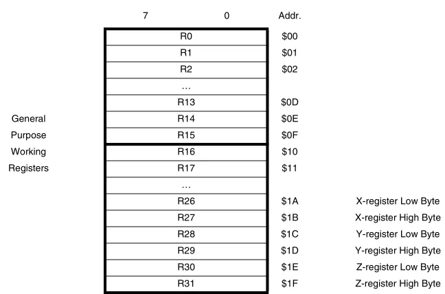
Figure 4. AVR CPU General Purpose Working Registers
Most of the instructions operating on the Register File have direct access to all registers, and most of them are single cycle instructions.
As shown in Figure 4, each register is also assigned a data memory address, mapping them directly into the first 32 locations of the user Data Space. Although not being phys-ically implemented as SRAM locations, this memory organization provides great flexibility in access of the registers, as the X-, Y-, and Z-pointer Registers can be set to index any register in the file.
The X-register, Y-register and Z-register
[image:35.612.224.548.87.301.2]The registers R26..R31 have some added functions to their general purpose usage. These registers are 16-bit address pointers for indirect addressing of the Data Space. The three indirect address registers X, Y, and Z are defined as described in Figure 5.
Figure 5. The X-, Y-, and Z-registers
In the different addressing modes these address registers have functions as fixed dis-placement, automatic increment, and automatic decrement (see the Instruction Set
7 0 Addr.
R0 $00
R1 $01
R2 $02
…
R13 $0D
General R14 $0E
Purpose R15 $0F
Working R16 $10
Registers R17 $11
…
R26 $1A X-register Low Byte
R27 $1B X-register High Byte
R28 $1C Y-register Low Byte
R29 $1D Y-register High Byte
R30 $1E Z-register Low Byte
R31 $1F Z-register High Byte
15 XH XL 0
X - register 7 0 7 0
R27 ($1B) R26 ($1A)
15 YH YL 0
Y - register 7 0 7 0
R29 ($1D) R28 ($1C)
15 ZH ZL 0
Z - register 7 0 7 0
Stack Pointer
The Stack is mainly used for storing temporary data, for storing local variables and for storing return addresses after interrupts and subroutine calls. The Stack Pointer Regis-ter always points to the top of the stack. Note that the stack is implemented as growing from higher memory locations to lower memory locations. This implies that a stack PUSH command decreases the Stack Pointer.The Stack Pointer points to the data SRAM stack area where the Subroutine and Inter-rupt Stacks are located. This Stack space in the data SRAM must be defined by the program before any subroutine calls are executed or interrupts are enabled. The Stack Pointer must be set to point above $60. The Stack Pointer is decremented by one when data is pushed onto the Stack with the PUSH instruction, and it is decremented by two when the return address is pushed onto the Stack with subroutine call or interrupt. The Stack Pointer is incremented by one when data is popped from the Stack with the POP instruction, and it is incremented by two when data is popped from the Stack with return from subroutine RET or return from interrupt RETI.
The AVR Stack Pointer is implemented as two 8-bit registers in the I/O space. The num-ber of bits actually used is implementation dependent. Note that the data space in some implementations of the AVR architecture is so small that only SPL is needed. In this case, the SPH Register will not be present.
Bit 15 14 13 12 11 10 9 8
SP15 SP14 SP13 SP12 SP11 SP10 SP9 SP8 SPH
SP7 SP6 SP5 SP4 SP3 SP2 SP1 SP0 SPL
7 6 5 4 3 2 1 0
Read/Write R/W R/W R/W R/W R/W R/W R/W R/W
R/W R/W R/W R/W R/W R/W R/W R/W
Initial Value 0 0 0 0 0 0 0 0
Instruction Execution
Timing
This section describes the general access timing concepts for instruction execution. The AVR CPU is driven by the CPU clock clkCPU, directly generated from the selected clock source for the chip. No internal clock division is used.
Figure 6 shows the parallel instruction fetches and instruction executions enabled by the Harvard architecture and the fast-access Register file concept. This is the basic pipelin-ing concept to obtain up to 1 MIPS per MHz with the correspondpipelin-ing unique results for functions per cost, functions per clocks, and functions per power-unit.
Figure 6. The Parallel Instruction Fetches and Instruction Executions
Figure 7 shows the internal timing concept for the Register file. In a single clock cycle an ALU operation using two register operands is executed, and the result is stored back to the destination register.
Figure 7. Single Cycle ALU Operation
Reset and Interrupt
Handling
The AVR provides several different interrupt sources. These interrupts and the separate reset vector each have a separate program vector in the program memory space. All interrupts are assigned individual enable bits which must be written logic one together with the Global Interrupt Enable bit in the Status Register in order to enable the interrupt. Depending on the program counter value, interrupts may be automatically disabled when Boot Lock bits BLB02 or BLB12 are programmed. This feature improves software security. See the section “Memory Programming” on page 254 for details.
clk
1st Instruction Fetch 1st Instruction Execute 2nd Instruction Fetch 2nd Instruction Execute 3rd Instruction Fetch 3rd Instruction Execute 4th Instruction Fetch
T1 T2 T3 T4
CPU
Total Execution Time
Register Operands Fetch
ALU Operation Execute
Result Write Back
T1 T2 T3 T4
– the External Interrupt Request 0. The Interrupt Vectors can be moved to the start of the Boot Flash section by setting the IVSEL bit in the General Interrupt Control Register (GICR). Refer to “Interrupts” on page 42 for more information. The Reset Vector can also be moved to the start of the boot Flash section by programming the BOOTRST fuse, see “Boot Loader Support – Read-While-Write Self-Programming” on page 241.
When an interrupt occurs, the Global Interrupt Enable I-bit is cleared and all interrupts are disabled. The user software can write logic one to the I-bit to enable nested inter-rupts. All enabled interrupts can then interrupt the current interrupt routine. The I-bit is automatically set when a Return from Interrupt instruction – RETI – is executed.
There are basically two types of interrupts. The first type is triggered by an event that sets the interrupt flag. For these interrupts, the Program Counter is vectored to the actual Interrupt Vector in order to execute the interrupt handling routine, and hardware clears the corresponding interrupt flag. Interrupt flags can also be cleared by writing a logic one to the flag bit position(s) to be cleared. If an interrupt condition occurs while the corresponding interrupt enable bit is cleared, the interrupt flag will be set and remem-bered until the interrupt is enabled, or the flag is cleared by software. Similarly, if one or more interrupt conditions occur while the Global Interrupt Enable bit is cleared, the cor-responding interrupt flag(s) will be set and remembered until the global interrupt enable bit is set, and will then be executed by order of priority.
The second type of interrupts will trigger as long as the interrupt condition is present. These interrupts do not necessarily have interrupt flags. If the interrupt condition disap-pears before the interrupt is enabled, the interrupt will not be triggered.
When the AVR exits from an interrupt, it will always return to the main program and exe-cute one more instruction before any pending interrupt is served.
Note that the Status Register is not automatically stored when entering an interrupt rou-tine, nor restored when returning from an interrupt routine. This must be handled by software.
When using the CLI instruction to disable interrupts, the interrupts will be immediately disabled. No interrupt will be executed after the CLI instruction, even if it occurs simulta-neously with the CLI instruction. The following example shows how this can be used to avoid interrupts during the timed EEPROM write sequence.
Assembly Code Example
in r16, SREG ; store SREG value
cli ; disable interrupts during timed sequence
sbiEECR, EEMWE ; start EEPROM write
sbiEECR, EEWE
outSREG, r16 ; restore SREG value (I-bit)
C Code Example
char cSREG;
cSREG = SREG; /* store SREG value */
When using the SEI instruction to enable interrupts, the instruction following SEI will be executed before any pending interrupts, as shown in this example.
Interrupt Response Time The interrupt execution response for all the enabled AVR interrupts is four clock cycles minimum. After four clock cycles the program vector address for the actual interrupt handling routine is executed. During this four clock cycle period, the Program Counter is pushed onto the Stack. The vector is normally a jump to the interrupt routine, and this jump takes three clock cycles. If an interrupt occurs during execution of a multi-cycle instruction, this instruction is completed before the interrupt is served. If an interrupt occurs when the MCU is in sleep mode, the interrupt execution response time is increased by four clock cycles. This increase comes in addition to the start-up time from the selected sleep mode.
A return from an interrupt handling routine takes four clock cycles. During these four clock cycles, the Program Counter (two bytes) is popped back from the Stack, the Stack Pointer is incremented by two, and the I-bit in SREG is set.
Assembly Code Example
sei ; set global interrupt enable
sleep; enter sleep, waiting for interrupt
; note: will enter sleep before any pending ; interrupt(s)
C Code Example
_SEI(); /* set global interrupt enable */
_SLEEP(); /* enter sleep, waiting for interrupt */
AVR ATmega16
Memories
This section describes the different memories in the ATmega16. The AVR architecture has two main memory spaces, the Data Memory and the Program Memory space. In addition, the ATmega16 features an EEPROM Memory for data storage. All three mem-ory spaces are linear and regular.
In-System
Reprogrammable Flash
Program Memory
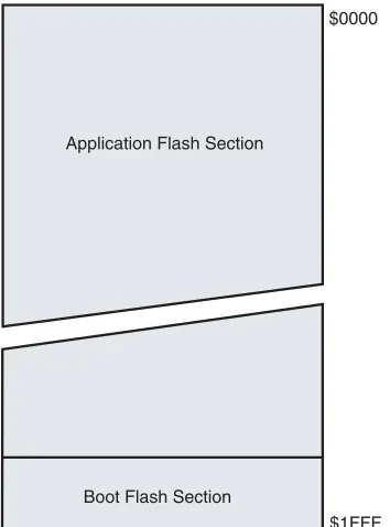
The ATmega16 contains 16K bytes On-chip In-System Reprogrammable Flash memory for program storage. Since all AVR instructions are 16 or 32 bits wide, the Flash is orga-nized as 8K x 16. For software security, the Flash Program memory space is divided into two sections, Boot Program section and Application Program section.
The Flash memory has an endurance of at least 10,000 write/erase cycles. The ATmega16 Program Counter (PC) is 13 bits wide, thus addressing the 8K program memory locations. The operation of Boot Program section and associated Boot Lock bits for software protection are described in detail in “Boot Loader Support – Read-While-Write Self-Programming” on page 241. “Memory Programming” on page 254 con-tains a detailed description on Flash data serial downloading using the SPI pins or the JTAG interface.
Constant tables can be allocated within the entire program memory address space (see the LPM – Load Program Memory Instruction Description).
[image:40.612.296.473.378.617.2]Timing diagrams for instruction fetch and execution are presented in “Instruction Execu-tion Timing” on page 11.
Figure 8. Program Memory Map
$0000
$1FFF Application Flash Section
SRAM Data Memory
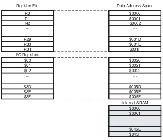
Figure 9 shows how the ATmega16 SRAM Memory is organized.The lower 1120 Data Memory locations address the Register file, the I/O Memory, and the internal data SRAM. The first 96 locations address the Register file and I/O Memory, and the next 1024 locations address the internal data SRAM.
The five different addressing modes for the data memory cover: Direct, Indirect with Dis-placement, Indirect, Indirect with Pre-decrement, and Indirect with Post-increment. In the Register file, registers R26 to R31 feature the indirect addressing pointer registers.
The direct addressing reaches the entire data space.
The Indirect with Displacement mode reaches 63 address locations from the base address given by the Y- or Z-register.
When using register indirect addressing modes with automatic pre-decrement and post-increment, the address registers X, Y, and Z are decremented or incremented.
[image:41.612.222.545.310.588.2]The 32 general purpose working registers, 64 I/O Registers, and the 1024 bytes of inter-nal data SRAM in the ATmega16 are all accessible through all these addressing modes. The Register file is described in “General Purpose Register File” on page 8.
Figure 9. Data Memory Map
Register File
R0 R1 R2
R29 R30 R31 I/O Registers
$00 $01 $02 ...
$3D $3E $3F ...
$0000 $0001 $0002
$001D $001E $001F
$0020 $0021 $0022 ...
$005D $005E $005F
... Data Address Space
$0060 $0061
$045E $045F
Data Memory Access Times This section describes the general access timing concepts for internal memory access. The internal data SRAM access is performed in two clkCPU cycles as described in Figure 10.
Figure 10. On-chip Data SRAM Access Cycles
EEPROM Data Memory
The ATmega16 contains 512 bytes of data EEPROM memory. It is organized as a sep-arate data space, in which single bytes can be read and written. The EEPROM has an endurance of at least 100,000 write/erase cycles. The access between the EEPROM and the CPU is described in the following, specifying the EEPROM Address Registers, the EEPROM Data Register, and the EEPROM Control Register.For a detailed description of SPI and JTAG data downloading to the EEPROM, see page 268 and page 272, respectively.
EEPROM Read/Write Access The EEPROM Access Registers are accessible in the I/O space.
The write access time for the EEPROM is given in Table 1. A self-timing function, how-ever, lets the user software detect when the next byte can be written. If the user code contains instructions that write the EEPROM, some precautions must be taken. In heavily filtered power supplies, VCC is likely to rise or fall slowly on Power-up/down. This causes the device for some period of time to run at a voltage lower than specified as minimum for the clock frequency used. See “Preventing EEPROM Corruption” on page 20 for details on how to avoid problems in these situations.
In order to prevent unintentional EEPROM writes, a specific write procedure must be fol-lowed. Refer to the description of the EEPROM Control Register for details on this.
When the EEPROM is read, the CPU is halted for four clock cycles before the next instruction is executed. When the EEPROM is written, the CPU is halted for two clock
clk
WR
RD Data
Data
Address Address Valid
T1 T2 T3
Compute Address
Read
Wr
ite
CPU
[image:42.612.222.542.131.342.2]The EEPROM Address
Register – EEARH and EEARL
• Bits 15..9 – Res: Reserved Bits
These bits are reserved bits in the ATmega16 and will always read as zero.
• Bits 8..0 – EEAR8..0: EEPROM Address
The EEPROM Address Registers – EEARH and EEARL – specify the EEPROM address
in the 512 bytes EEPROM space. The EEPROM data bytes are addressed linearly between 0 and 511. The initial value of EEAR is undefined. A proper value must be writ-ten before the EEPROM may be accessed.
The EEPROM Data Register – EEDR
• Bits 7..0 – EEDR7.0: EEPROM Data
For the EEPROM write operation, the EEDR Register contains the data to be written to the EEPROM in the address given by the EEAR Register. For the EEPROM read oper-ation, the EEDR contains the data read out from the EEPROM at the address given by EEAR.
The EEPROM Control Register – EECR
• Bits 7..4 – Res: Reserved Bits
These bits are reserved bits in the ATmega16 and will always read as zero.
• Bit 3 – EERIE: EEPROM Ready Interrupt Enable
Writing EERIE to one enables the EEPROM Ready Interrupt if the I bit in SREG is set. Writing EERIE to zero disables the interrupt. The EEPROM Ready interrupt generates a constant interrupt when EEWE is cleared.
• Bit 2 – EEMWE: EEPROM Master Write Enable
Bit 15 14 13 12 11 10 9 8
– – – – – – – EEAR8 EEARH
EEAR7 EEAR6 EEAR5 EEAR4 EEAR3 EEAR2 EEAR1 EEAR0 EEARL
7 6 5 4 3 2 1 0
Read/Write R R R R R R R R/W
R/W R/W R/W R/W R/W R/W R/W R/W
Initial Value 0 0 0 0 0 0 0 X
X X X X X X X X
Bit 7 6 5 4 3 2 1 0
MSB LSB EEDR
Read/Write R/W R/W R/W R/W R/W R/W R/W R/W
Initial Value 0 0 0 0 0 0 0 0
Bit 7 6 5 4 3 2 1 0
– – – – EERIE EEMWE EEWE EERE EECR
Read/Write R R R R R/W R/W R/W R/W
When EEMWE has been written to one by software, hardware clears the bit to zero after four clock cycles. See the description of the EEWE bit for an EEPROM write procedure.
• Bit 1 – EEWE: EEPROM Write Enable
The EEPROM Write Enable Signal EEWE is the write strobe to the EEPROM. When address and data are correctly set up, the EEWE bit must be written to one to write the value into the EEPROM. The EEMWE bit must be written to one before a logical one is written to EEWE, otherwise no EEPROM write takes place. The following procedure should be followed when writing the EEPROM (the order of steps 3 and 4 is not essential):
1. Wait until EEWE becomes zero.
2. Wait until SPMEN in SPMCR becomes zero. 3. Write new EEPROM address to EEAR (optional). 4. Write new EEPROM data to EEDR (optional).
5. Write a logical one to the EEMWE bit while writing a zero to EEWE in EECR. 6. Within four clock cycles after setting EEMWE, write a logical one to EEWE.
The EEPROM can not be programmed during a CPU write to the Flash memory. The software must check that the Flash programming is completed before initiating a new EEPROM write. Step 2 is only relevant if the software contains a Boot Loader allowing the CPU to program the Flash. If the Flash is never being updated by the CPU, step 2 can be omitted. See “Boot Loader Support – Read-While-Write Self-Programming” on page 241 for details about boot programming.
Caution: An interrupt between step 5 and step 6 will make the write cycle fail, since the EEPROM Master Write Enable will time-out. If an interrupt routine accessing the EEPROM is interrupting another EEPROM Access, the EEAR or EEDR reGister will be modified, causing the interrupted EEPROM Access to fail. It is recommended to have the global interrupt flag cleared during all the steps to avoid these problems.
When the write access time has elapsed, the EEWE bit is cleared by hardware. The user software can poll this bit and wait for a zero before writing the next byte. When EEWE has been set, the CPU is halted for two cycles before the next instruction is executed.
• Bit 0 – EERE: EEPROM Read Enable
The EEPROM Read Enable Signal – EERE – is the read strobe to the EEPROM. When the correct address is set up in the EEAR register, the EERE bit must be written to a logic one to trigger the EEPROM read. The EEPROM read access takes one instruction, and the requested data is available immediately. When the EEPROM is read, the CPU is halted for four cycles before the next instruction is executed.
The user should poll the EEWE bit before starting the read operation. If a write operation is in progress, it is neither possible to read the EEPROM, nor to change the EEAR register.
Note: 1. Uses 1 MHz clock, independent of CKSEL Fuse setting.
The following code examples show one assembly and one C function for writing to the EEPROM. The examples assume that interrupts are controlled (for example by dis-abling interrupts globally) so that no interrupts will occur during execution of these functions. The examples also assume that no Flash Boot Loader is present in the soft-ware. If such code is present, the EEPROM write function must also wait for any ongoing SPM command to finish.
Assembly Code Example
EEPROM_write:
; Wait for completion of previous write
sbic EECR,EEWE
rjmp EEPROM_write
; Set up address (r18:r17) in address register
out EEARH, r18
out EEARL, r17
; Write data (r16) to data register
out EEDR,r16
; Write logical one to EEMWE
sbi EECR,EEMWE
; Start eeprom write by setting EEWE
sbi EECR,EEWE
ret
C Code Example
void EEPROM_write(unsigned int uiAddress, unsigned char ucData)
{
/* Wait for completion of previous write */ while(EECR & (1<<EEWE))
;
/* Set up address and data registers */ EEAR = uiAddress;
EEDR = ucData;
/* Write logical one to EEMWE */
EECR |= (1<<EEMWE);
/* Start eeprom write by setting EEWE */
The next code examples show assembly and C functions for reading the EEPROM. The examples assume that interrupts are controlled so that no interrupts will occur during execution of these functions.
Preventing EEPROM Corruption
During periods of low VCC, the EEPROM data can be corrupted because the supply volt-age is too low for the CPU and the EEPROM to operate properly. These issues are the same as for board level systems using EEPROM, and the same design solutions should be applied.
An EEPROM data corruption can be caused by two situations when the voltage is too low. First, a regular write sequence to the EEPROM requires a minimum voltage to operate correctly. Secondly, the CPU itself can execute instructions incorrectly, if the supply voltage is too low.
E EP R O M da ta c o r r up ti on ca n e as i l y b e av o id ed by fo ll o wi ng t hi s de si g n recommendation:
Keep the AVR RESET active (low) during periods of insufficient power supply volt-age. This can be done by enabling the internal Brown-out Detector (BOD). If the Assembly Code Example
EEPROM_read:
; Wait for completion of previous write
sbic EECR,EEWE
rjmp EEPROM_read
; Set up address (r18:r17) in address register
out EEARH, r18
out EEARL, r17
; Start eeprom read by writing EERE
sbi EECR,EERE
; Read data from data register
in r16,EEDR
ret
C Code Example
unsigned char EEPROM_read(unsigned int uiAddress)
{
/* Wait for completion of previous write */
while(EECR & (1<<EEWE)) ;
/* Set up address register */ EEAR = uiAddress;
/* Start eeprom read by writing EERE */
EECR |= (1<<EERE);
/* Return data from data register */
I/O Memory
The I/O space definition of the ATmega16 is shown in “Register Summary” on page 298.All ATmega16 I/Os and peripherals are placed in the I/O space. The I/O locations are accessed by the IN and OUT instructions, transferring data between the 32 general purpose working registers and the I/O space. I/O Registers within the address range $00 -$1F are directly bit-accessible using the SBI and CBI instructions. In these registers, the value of single bits can be checked by using the SBIS and SBIC instructions. Refer to the Instruction Set section for more details. When using the I/O specific commands IN and OUT, the I/O addresses $00 - $3F must be used. When addressing I/O Registers as data space using LD and ST instructions, $20 must be added to these addresses.
For compatibility with future devices, reserved bits should be written to zero if accessed. Reserved I/O memory addresses should never be written.
Some of the status flags are cleared by writing a logical one to them. Note that the CBI and SBI instructions will operate on all bits in the I/O Register, writing a one back into any flag read as set, thus clearing the flag. The CBI and SBI instructions work with reg-isters $00 to $1F only.
System Clock and
Clock Options
Clock Systems and their
Distribution
Figure 11 presents the principal clock systems in the AVR and their distribution. All of the clocks need not be active at a given time. In order to reduce power consumption, the clocks to modules not being used can be halted by using different sleep modes, as described in “Power Management and Sleep Modes” on page 30. The clock systems are detailed Figure 11.
Figure 11. Clock Distribution
CPU Clock – clkCPU The CPU clock is routed to parts of the system concerned with operation of the AVR
core. Examples of such modules are the General Purpose Register File, the Status Reg-ister and the data memory holding the Stack Pointer. Halting the CPU clock inhibits the core from performing general operations and calculations.
I/O Clock – clkI/O The I/O clock is used by the majority of the I/O modules, like Timer/Counters, SPI, and
USART. The I/O clock is also used by the External Interrupt module, but note that some external interrupts are detected by asynchronous logic, allowing such interrupts to be detected even if the I/O clock is halted. Also note that address recognition in the TWI module is carried out asynchronously when clkI/O is halted, enabling TWI address
recep-General I/O Modules Asynchronous
Timer/Counter ADC CPU Core RAM
clkI/O
clkASY
AVR Clock Control Unit
clkCPU
Flash and EEPROM
clkFLASH
clkADC
Source Clock
Watchdog Timer
Watchdog Oscillator Reset Logic
Clock Multiplexer
Watchdog Clock
Calibrated RC Oscillator Timer/Counter
Oscillator
Crystal Oscillator
Low-frequency Crystal Oscillator External RC
Oscillator
[image:48.612.192.566.200.494.2]Asynchronous Timer Clock – clkASY
The Asynchronous Timer clock allows the Asynchronous Timer/Counter to be clocked directly from an external 32 kHz clock crystal. The dedicated clock domain allows using this Timer/Counter as a real-time counter even when the device is in sleep mode.
ADC Clock – clkADC The ADC is provided with a dedicated clock domain. This allows halting the CPU and I/O clocks in order to reduce noise generated by digital circuitry. This gives more accu-rate ADC conversion results.
Clock Sources
The device has the following clock source options, selectable by Flash Fuse bits as shown below. The clock from the selected source is input to the AVR clock generator, and routed to the appropriate modules.Note: 1. For all fuses “1” means unprogrammed while “0” means programmed.
The various choices for each clocking option is given in the following sections. When the CPU wakes up from Power-down or Power-save, the selected clock source is used to time the start-up, ensuring stable Oscillator operation before instruction execution starts. When the CPU starts from Reset, there is as an additional delay allowing the power to reach a stable level before commencing normal operation. The Watchdog Oscillator is used for timing this real-time part of the start-up time. The number of WDT Oscillator cycles used for each time-out is shown in Table 3. The frequency of the Watchdog Oscillator is voltage dependent as shown in “ATmega16 Typical Characteristics – Pre-liminary Data” on page 293. The device is shipped with CKSEL = “0001” and SUT = “10” (1 MHz Internal RC Oscillator, slowly rising power).
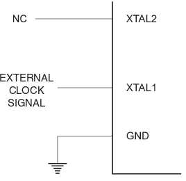
Crystal Oscillator
XTAL1 and XTAL2 are input and output, respectively, of an inverting amplifier which can be configured for use as an On-chip Oscillator, as shown in Figure 12. Either a quartz crystal or a ceramic resonator may be used. The CKOPT Fuse selects between two dif-ferent Oscillator amplifier modes. When CKOPT is programmed, the Oscillator output will oscillate will a full rail-to-rail swing on the output. This mode is suitable when operat-ing in a very noisy environment or when the output from XTAL2 drives a second clock buffer. This mode has a wide frequency range. When CKOPT is unprogrammed, the Oscillator has a smaller output swing. This reduces power consumption considerably.Table 2. Device Clocking Options Select(1)
Device Clocking Option CKSEL3..0
External Crystal/Ceramic Resonator 1111 - 1010
External Low-frequency Crystal 1001
External RC Oscillator 1000 - 0101
Calibrated Internal RC Oscillator 0100 - 0001
External Clock 0000
Table 3. Number of Watchdog Oscillator Cycles
Typ Time-out (VCC = 5.0V) Typ Time-out (VCC = 3.0V) Number of Cycles
4.1 ms 4.3 ms 4K (4,096)
and resonators. The optimal value of the capacitors depends on the crystal or resonator in use, the amount of stray capacitance, and the electromagnetic noise of the environ-ment. Some initial guidelines for choosing capacitors for use with crystals are given in Table 4. For ceramic resonators, the capacitor values given by the manufacturer should be used. For more information on how to choose capacitors and other details on Oscilla-tor operation, refer to the Multi-purpose OscillaOscilla-tor application note.
Figure 12. Crystal Oscillator Connections
The Oscillator can operate in three different modes, each optimized for a specific fre-quency range. The operating mode is selected by the fuses CKSEL3..1 as shown in Table 4.
Note: 1. This option should not be used with crystals, only with ceramic resonators.
Table 4. Crystal Oscillator Operating Modes
CKOPT CKSEL3..1
Frequency Range (MHz)
Recommended Range for Capacitors C1 and C2 for Use with Crystals (pF)
1 101(1) 0.4 - 0.9 –
1 110 0.9 - 3.0 12 - 22
1 111 3.0 - 8.0 12 - 22
0 101, 110, 111 1.0 ≤ 12 - 22
XTAL2
XTAL1
GND C2
[image:50.612.321.443.170.279.2]The CKSEL0 Fuse together with the SUT1..0 fuses select the start-up times as shown in Table 5.
Notes: 1. These options should only be used when not operating close to the maximum
fre-quency of the device, and only if frefre-quency stability at start-up is not important for the application. These options are not suitable for crystals.
2. These options are intended for use with ceramic resonators and will ensure fre-quency stability at start-up. They can also be used with crystals when not operating close to the maximum frequency of the device, and if frequency stability at start-up is not important for the application.
Table 5. Start-up Times for the Crystal Oscillator Clock Selection
CKSEL0 SUT1..0
Start-up Time from Power-down and
Power-save
Additional Delay from Reset
(VCC = 5.0V) Recommended Usage
0 00 258 CK(1) 4.1 ms Ceramic resonator, fast
rising power
0 01 258 CK(1) 65 ms Ceramic resonator, slowly
rising power
0 10 1K CK(2) – Ceramic resonator, BOD
enabled
0 11 1K CK(2) 4.1 ms Ceramic resonator, fast
rising power
1 00 1K CK(2) 65 ms Ceramic resonator, slowly
rising power
1 01 16K CK – Crystal Oscillator, BOD
enabled
1 10 16K CK 4.1 ms Crystal Oscillator, fast
rising power
1 11 16K CK 65 ms Crystal Oscillator, slowly
Low-frequency Crystal
Oscillator
To use a 32.768 kHz watch crystal as the clock source for the device, the Low-fre-quency Crystal Oscillator must be selected by setting the CKSEL fuses to “1001”. The crystal should be connected as shown in Figure 12. By programming the CKOPT Fuse, the user can enable internal capacitors on XTAL1 and XTAL2, thereby removing the need for external capacitors. The internal capacitors have a nominal value of 36 pF. Refer to the 32 kHz Crystal Oscillator application note for details on Oscillator operation and how to choose appropriate values for C1 and C2.
When this Oscillator is selected, start-up times are determined by the SUT fuses as shown in Table 6.
Note: 1. These options should only be used if frequency stability at start-up is not important for
the application.
External RC Oscillator
For timing insensitive applications, the external RC configuration shown in Figure 13 can be used. The frequency is roughly estimated by the equation f = 1/(3RC). C should be at least 22 pF. By programming the CKOPT Fuse, the user can enable an internal 36 pF capacitor between XTAL1 and GND, thereby removing the need for an external capacitor. For more information on Oscillator operation and details on how to choose R and C, refer to the External RC Oscillator application note.Figure 13. External RC Configuration
The Oscillator can operate in four different modes, each optimized for a specific fre-quency range. The operating mode is selected by the fuses CKSEL3..0 as shown in Table 7.
Table 6. Start-up Times for the Low-frequency Crystal Oscillator Clock Selection
SUT1..0
Start-up Time from Power-down and
Power-save
Additional Delay from Reset
(VCC = 5.0V) Recommended Usage
00 1K CK(1) 4.1 ms Fast rising power or BOD enabled
01 1K CK(1) 65 ms Slowly rising power
10 32K CK 65 ms Stable frequency at start-up
11 Reserved
XTAL2
XTAL1
GND C
R VCC
[image:52.612.318.448.461.578.2]When this Oscillator is selected, start-up times are determined by the SUT fuses as shown in Table 8.
Note: 1. This option should not be used when operating close to the maximum frequency of
the device.
Calibrated Internal RC
Oscillator
The Calibrated Internal RC Oscillator provides a fixed 1.0, 2.0, 4.0, or 8.0 MHz clock. All frequencies are n