I
DESIGN OF SUBWOOFER AMPLIFIER
AIDAWATI BTE MUSTAPHA
Universiti Malaysia Sarawak
1998
TK
6565 A55
A288
Dorana Penyerahan Tesis Universiti Malaysia Sarawak
R13a
DORANG PENYERAHAN TESIS
Judul: DESIGN OF A SUBWOOFER AMPLIFIER
SESI PENGAJIAN: 1998/1999
Saya AIDAWATI BTE MUSTAPHA
(HURUF BESAR)
mengaku membenarkan tesis ini disimpan di Pusat Khidmat Maklwnat Akademik, Universiti Malaysia Sarawak dengan syarat-syarat kegunaan seperti be:ribt:
1. Hakmilik. k.ertas projek adaIah di bawah nama penulis melainkan penulisan sebagai projek. bersama dan dibiayai oleh UNIMAS, hakmiliknya adalah kepunyaan UNIMAS.
2. Naskhah salinan di dalam bentuk kertas atau mikro hanya boleh diboat dengan kebenaran bertulis
daripada penulis.
3. Pusat Khidmat Maldwnat Akademik, UNIMAS dibenarkan membuat salinan Wltuk pengajian mereu.
4. Kertas projek. hanya boleh di1eIbitkan dengan kebenaran penulis. Bayaran royalti adalah mengikut kadar yang diperserujui kelak.
5. • Saya ~tidakmembenarkan Perpustakaan membuat salinan kertas projek ini sebagai bahan pertukaran di antara institusi pengajian tinggi.
I 6. •• Sila tandakan ( .t )
[:=JSULIT (Mengandungi maklumat yang berdarjah kese1amatan stau kepentingan Malaysia seperti yang termaktub di dalam AKTA RAHSIA RASMlI972).
c:=:J
TERHAD (MengandWlgi maklwnat TERHAD yang telah ditentukan oleh organisasilbadan di mana penyelidikan dija1ankan). ~ TIDAK. TERHAD
Disahkan oleh
(TANDATANGAN PENULIS)
.'
(TANDAT ANGAN PENYELIA)Alamat tetap: NO 300A LORONG 6A1
TAMAN MATANGJAYA EN. NG LIANG YEW
Nama Penyelia 93050 JALAN MATANG. KUCHING
Tarikh: 12 HB OKTOBER, 1998 Tarikh: 12 HB OKTOBER, 1998
CATATAN * Potoq YIIIII ttdak berlreaaan.
** Jika KeJ1u ProJek Ini SULIT atau TERRAD, .... hunpirkan nrat daripluIa pihak berk1lasal
orpabasl berIre_ denpn menyertakan sekaU telDpoh krl1as proJek. Ini perlu dJkeIasl!.l sebapl SULIT atau TERHAD.
Tesis ini telah dibaca dan disahkan oleh :
• • • • • • • •• • 0 ' • • •• • • • 0 . ' 0 ' • •• • 0 • • •• • • • • • •
Tarikh (Mr. Ng Liang Yew)
P~~~~~~1T7~ALMakium
a
t
Akademik AYSIA SARAWAKDESIGN OF SUBWOOFER AMPLIFIER
AIDAWATI BTE MUSTAPHA
Tesis Dikemukakan Kepada
Fakulti Kejuruteraan, Universiti Malaysia Sarawak Sebagai Memenuhi Sebahagian daripada Syarat
Penganugerahan Sarjana Muda Kejuruteraan
Dengan Kepujian (Kejuruteraan Elektronik dan Telekomunikasi) 1998
Dedications
This thesis is dedicated with deepest love and affection to my beloved parent, Mustapha Bill Melek and Hadrah Bte Hj. Le1lltlll, brother andsister. Their love, patience, guidance, wisdom and strenght have inspired me throughout the three anda halfyears in
University Malaysia Sarawak to be the best that I can be
Acknowledgement
Firstly, the author would like to express his grateful to Allah Almighty, only with
His
guidance the author can complete this project.The author would like to express his deepest thanks to all the people who had given their support to make this project. The author's greatest appreciation to the project supervisor : Mr. Ng Liang Yew for his worthy suggestions and invaluable knowledge shared with the author during this project guidance.
Lastly, the author wishes to convey his sincere gratefulness to his family members and friends for their support and endless encouragement.
J iii
Abstract
Nowadays'subwoofer amplifier' has a potential to expand. It is a support system to audio video system especially in the using of multimedia. The audio system which is always used in the multimedia could not give a dramatic effect such as bomb explosion
and earthquake. To have this effect the designed will concentrate only to amplifier
vibration effect while sound effect is neglected. The sound effect can be found from other
audio amplifier system which will be used together with subwoofer amplifier.
The basic design is divided into three parts as to achieve the desired goal. There are as below ;
I. filter
u. amplifier
III. supply voltage
Active components which mostly used in this project are semiconductor in the form of operational amplifier and integrated circuit. Other semiconductor component used is
transistor. The use of operational ~plifier and integrated circuit have eased the project
carried out because it only required simple external connection.
Abstrak
'Subwoofer Amplifier' mempunyai potensi untuk berkembang pada masa kini.
Ianya merupakan sistem sokongan kepada sistem audio video terutamanya dalam
penggunaan multimedia. Biasanya sistem audio yang terdapat dalam multimedia tidak
dapat memberi kesan yang dramatik untuk sesetengah keadaan seperti apabila born meletup ataupun gempa bumi berlaku. Penggunaan sistem subwoofer dijangka dapat membantu menambahkan kesan dramatik ini. Bagi mendapatkan kesan ini penguat yang
direka hanya menitikberatkan kesan gegaran manakala kesan bunyi tidak diperlukan.
Kesan bunyi boleh didapati oleh sistem penguat audio lain yang akan digunakan
bersama-sama dengan sistem subwoofer ini.
Bagi mencapai matlamat diatas keperluan asas rekabentuk adalah terbahagi kepada tiga bahagian utama iaitu :
i) bahagian penapis
ii) bahagian penguat
iii) bahagian voltan bekalan
Kebanyakan komponen aktif yangi-isunakan dalam projek ini adalah separa pengalir dalam bentuk penguat kendali dan Iitar bersepadu. Bahan separa pengalir lain yang digunakan adalah transistor. Penggunaan penguat kendali dan litar bersepadu memudahkan projek ini dijalankan kerana ia memerlukan sambungan luaran yang mudah.
Pusat Khidmat Makiumat Akademik
VNIVERSITI MALAYSIA SARAWAK
TABLE OF CONTENTS Pages Title page ii Dedication Acknowledgement 111 iv Abstract Abstrak v Vl Tables of Contents List of Figures Vll Xl List of Tables
List of Symbols and Abbreviations X111
Chapter 1 : Introduction 1.1 Introduction
..
:,. 1 1 1.2 Objective 2 1.3 Project Overview 3 1.4 Outline of thesis viChapter 2 : Active Filter Design
2
.
1
Active filter 42
.
2
Basic active filter design 42
.
3
Low pass filter design7
2.4
Gain and phase shift of the circuit 102
.
5
The VCVS high pass filter 112
.
6
Fourth order high pass filter 132.6.1
First stage design15
2.6
.
2
Second stage design16
2
.
7
Fourth Order low pass filter design19
2.7.1
First stage low pass filter design19
2
.
7
.
2
Second stage low pass filter design20
2
.
8
Complete band pass filter design23
Chapter 3 : Power amplifier
3.1
Power amplifier25
3
.
2
Power bridging26
3
.
3
Power amplifier desiJa,28
3
.
3
.
1
The inverting amplifier30
3
.
3
.
2
Non inverting amplifier31
Chapter 4 : Power supply
4.1 Introduction of power supply 4.2 Constant voltage supplies 4.3 Basic stabilizing circuit 4.4 Load regulation
4.5 Voltage regulator 4.5.1 Load effect
4.5.2 Dual transformer power supply 4.5.3 Design ±12V power supply 4.5.4 Design ±15V 4.6A power supply 4.6 Component selection
Chapter 5 : Circuit Implementation and testing 5.1 Design requirement
5.2 Matching input and output signal 5.3 Transistor heat sinking
Chapter 6 : Suggestion Chapter 7: .Conclusion References 36 36 37 38 41 42 43 43 44 44 52 53 58 63 64 66 viii
l
IIr
Figure la Figure 2a Figure 2b Figure 2c Figure 2d Figure 2e Figure 2f Figure 3a Figure 3b Figure 3c Figure 3d Figure 3e Figure 4a Figure 4b Figure 4c Figure4d Figure 4e Figure 4f Figure 4g UST OF FIGURESTitle of Figures Pages
Overviews of musical processing signal 2
Sallen Key Second order filter 5
Redrawn circuit for dc condition 9
Circuit diagram for high pass filter 11
Cascading filter to obtain higher order filter 14
Schematic diagram for the band pass filter 22
Frequency response of the band pass filter 24
The signals involved in parallel bridging 27
Inverting amplifier 29
Non inverting amplifier 30
Schematic diagram of the amplifier 34
Mounting power op amp module at the chassis as heat
sinking 35
Response characteristics of power supply 37
Line regulation in ~relationship between Vin and V out 40
How regulators fit into power supply scheme 41
Schematic diagram of the voltage supply 46
DC pulse waveform of rectifier 47
Output voltage from filtering capacitor 48
Dual supply with dual transformer 51
ix
Figure 5a Instrument set up for evaluation of amplifier 54 Figure 5b Testing the filter with a music signal with the volume
control is set to maximum 54
Figure 5c Square wave test 55
Figure 5d Output from the power amplifiers 56
Figure 5e Maximum swing of music signal 57
Figure 5f Mounting the transistor on the heat sink 62
.'
LIST OF TABLES
Title of tables Page
Table Sa
Table 5b
Junction to ambient thermal resistance's
Thermal resistance between the transistor case and heat sink.
59
60
/ VI Vo V Av Is Ircp I Opamp
UST OF SYMBOL AND ABBREVIAnONS
input voltage output volatge voltage voltage gain surge current repetitive current current operational amplifier xiii
CHAPTER 1 INTRODUCTION
1.1 IDtroductioa
Subwoofer Amplifier is an amplifier which amplify subsonic frequency. Subsonic frequency also known as infra bass frequency and no sound generated at this frequency. But we can feel the vibration from this kind of frequency. An
amplifier should be used to generate enough vibration which can fell by the user. The subwoofer amplifier will be combine with other audio systems. It mainly being used as a part of multimedia system. The realistic sound system combined with a subwoofer system will greatly enhance the overall performance of the multimedia system.
1.2 Objective
Objective of this project is to design and built an amplifier which can produce vibrations that cannot be heard. The sound effect will be reduced as much
'tt~,
as possible. The working frequencies choosed in this project are 5Hz to 40Hz, a very low frequency range. This frequency range is chosen because we do not want any dc components which affect the quality of vibration. A frequency higher than 40Hz will be and this will not fulfill system requirements.
,
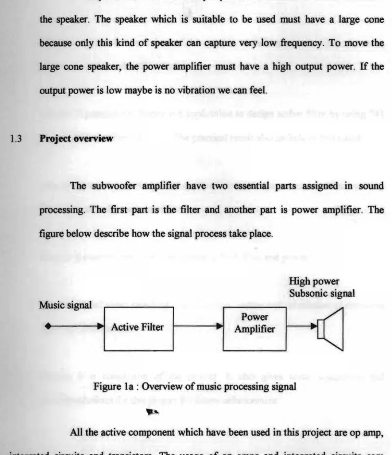
An amplifier have 60 watts output power are decided to be built to movethe speaker. The speaker which is suitable to be used must have a large cone because only this kind of speaker can capture very low frequency. To move the large cone speaker, the power amplifier must have a high output power. If the output power is low maybe is no vibration we can feel.
1.3 Project overview
The subwoofer amplifier have two essential parts assigned in sound processing. The first part is the filter and another part is power amplifier. The figure below describe how the signal process take place.
High power Subsonic signal
M.USiC signal
"'1
Power.->---I....
~- Active Filter•
I
Amplifier
Figure la : Overview of music processing signal
All the active component which have been used in this project are op amp, integrated circuits and transistors. The usage of op amps and integrated circuits cam
simplify the circuits design and also they can reduce the cost of this project.
1.4 Outline of thesis
Chapter 1 gives the overview of this project including introduction, objective, project structure and outline thesis.
Chapter 2 presents the theory and application to design active filter by using 741 operational amplifier (op amp). The practical result also include in this chapter.
Chapter 3 presents the theory and applications to design power amplifier by using L465 operational power amplifier.
Chapter 4 concentrates on power supply to both filter and power amplifier.
Chapter 5 brief about matching overall design, testing and calculation of the result achieved from the test.
Chapter 6 is conclusion of the project. It also gives some suggestion and recommendations for this ~~ject for future enhancement.
Pusal Khidmat Maklumat Akademik
UNIVERSITI MALAYStA SARAWAK /
CHAPTER 2
ACTIVE FILTER DESIGN
2.1 Active fdter
Since subwoofer amplifier need a frequency range between 5Hz to 40Hz, it is necessary to make a filter which operates at that frequency. At that frequency range the frequency lower than 5Hz and higher than 40Hz will be attenuated. This frequency range is enough to fulfill the needs of subwoofer amplifier design which means remove the sound from the amplifier.
The type of active filter have been designed In butterworth filter. Butterworth filter is expected to be suitable to fit in this application because of it's flat response in the pass band region. Fourth order filter is choose because this order have rapid attenuation in roll off region. This action will keep more desired frequency and removed unwanted frequency.
2.2 Basic active fdter design
..
'
,
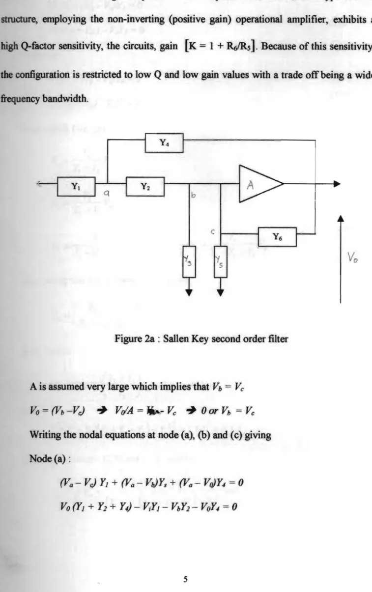
The most popular active filter is using voltage control voltage source (VCVS) method. This type of circuits was first proposed by Sail en and Key and it is relatively
easy to design and implement. Figure 2a illustrates about SaIlen key second order filter. It
employs the infinite gain VCVS concepts associated with the operational amplifier and
L'
I'
t
the
circuits offers external gain adjustment via components Ys and Y6. This type of filterstructure, employing the non-inverting (positive gain) operational amplifier, exhibits a high Q-factor sensitivity, the circuits, gain [K = 1 +
RdRsl
Because of this sensitivity, the configuration is restricted to low Q and low gain values with a trade off being a wide frequency bandwidth.Y4
I
I
II
b C...
~
Y2 Y.I
ql
~
i
~~ Y6l
Vo
rt~ 'isFigure 2a : Sallen Key second order filter
A is assumed very large which implies that Vb = Vc
Writing the nodal equations at node (a), (b) and (c) giving Node (a) :
5
Node (b)
v"f! + (V" - VcJY1 = 0
Node (C)
From which (we get)
Y.
V
= 6V
C y.+y. 0
5 6
substituting this into equation (2.6) yields
from which (2.2) (2.3) (2.4) (2.5) (2.6) (2.7) that is (2.8)
Equating equations (2.5) and ( 2.8) yields
6
Filially ;lIter same manipulation. we obtain the expression
v
o(2.9)
2.3 Low Pass Filter Design
Here
I
Y =
I R '
I
from the I!quation (2 .9)
manipulation of the expression yields
'tl~
Now K = I + R4!R3 which is the de gain of the stage and the expression may finally
be written as
t
if we note further that W 2
=
I then we may compare equation o C)C2 R)R3(2.1 0) with the standard fonn for a second-order low pass filter
(2.11)
Where COo is the 3 dB frequency for the Butterwoth case and bocoo is the frequency at the end of the ripple band for the Chebyshev filter. The coefficients bo ,
bo , etc. are the appropriate coefficients for the prescribed filter response.
Comparison between equation (2.10) and (2.11) yields
(2.12)
We must now introduce normalization into the components and design
parameters in order to produced a rationalized design procedure. Let co0
2
= 1 radls,
C,= C2 = I farad. Then the equation (2.12) becomes
.~, I bo = R)R2 (2.13) 1 1 b - - +- (2-K) 1 - R, R2
Now we know that there are six unknowns and therefor a certain degree of
component selectivity will have to be made since a unique solution is not possible.
From equation (2.13) we obtain
(2- K) hi = b"R2 + R
2
which may be written as
and which has a solution
(2.14)
So far we have nonnalized the capacitor C1 , C2 and obtained the nonnalized
values for the resistors R\ , R2, we now have to obtain values for the gain resistors R3
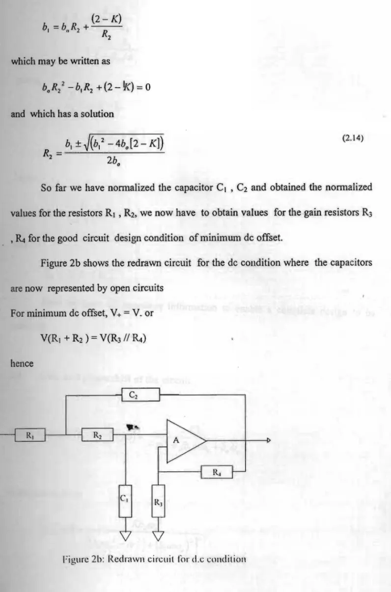
, It, for the good circuit design condition of minimum dc offset.
Figure 2b shows the redrawn circuit for the dc condition where the capacitors are now represented by open circuits
For minimum dc offset, V+
=
V_ orhence
Figure 2b: Redrawn circuit fol' d.c condition