copied or distributed.
The Design Warrior’s
Guide to FPGAs
200 Wheeler Road, Burlington, MA 01803, USA
Linacre House, Jordan Hill, Oxford OX2 8DP, UK
Copyright © 2004, Mentor Graphics Corporation and Xilinx, Inc. All rights reserved.
Illustrations by Clive “Max” Maxfield
No part of this publication may be reproduced, stored in a retrieval system, or trans-mitted in any form or by any means, electronic, mechanical, photocopying,
recording, or otherwise, without the prior written permission of the publisher.
Permissions may be sought directly from Elsevier’s Science & Technology Rights Department in Oxford, UK: phone: (+44) 1865 843830, fax: (+44) 1865 853333, e-mail: [email protected]. You may also complete your request on-line via the Elsevier homepage (http://elsevier.com), by selecting “Customer Support” and then “Obtaining Permissions.”
Recognizing the importance of preserving what has been written, Elsevier prints its books on acid-free paper whenever possible.
Library of Congress Cataloging-in-Publication Data
A catalog record for this book is available from the Library of Congress.
ISBN: 0-7506-7604-3
British Library Cataloguing-in-Publication Data
A catalogue record for this book is available from the British Library.
For information on all Newnes publications
visit our Web site at www.newnespress.com
04 05 06 07 08 09 10 9 8 7 6 5 4 3 2 1
and rainbow-colored sprinkles on the ice cream sundae of my life
searchable copy ofThe Design Warrior’s Guide to FPGAsin Adobe Acrobat (PDF) format. You can copy this PDF to your computer so as to be able to access The Design Warrior’s Guide to FPGAsas required (this is particularly useful if you travel a lot and use a notebook computer).
The CD also contains a set of Microsoft®PowerPoint®files—one for each chapter and appendix—containing copies of the illustrations that are festooned throughout the book. This will be of particular interest for educators at colleges and universities when it comes to giving lectures or creating handouts based onThe Design Warrior’s Guide to FPGAs
Preface . . . ix
A simple programmable function . 9 Fusible link technologies . . . 10
Antifuse technologies . . . 12
Mask-programmed devices . . . . 14
PROMs . . . 15
EPROM-based technologies . . . 17
EEPROM-based technologies . . 19
FLASH-based technologies . . . 20
SRAM-based technologies . . . . 21
Summary . . . 22 Alternative FPGA Architectures 57 A word of warning . . . 57
A little background information . 57 Antifuse versus SRAM versus … . . . 59
Fine-, medium-, and coarse-grained architectures . . . 66
MUX- versus LUT-based logic blocks . . . 68
CLBs versus LABs versus slices. . 73
Fast carry chains . . . 77
Clock trees and clock managers . 84 General-purpose I/O . . . 89
Gigabit transceivers . . . 92
Hard IP, soft IP, and firm IP . . . 93
System gates versus real gates . . 95
Chapter 5
Using the configuration port . . 105
Using the JTAG port . . . 111
Using an embedded processor. . 113
Chapter 6
FPGA-specialist and independent EDA vendors . . . 117
FPGA design consultants with special tools . . . 118
Open-source, free, and low-cost design tools . . . 118
Pipelining and levels of logic . . 122
Asynchronous design practices . 126 Clock considerations . . . 127
Register and latch considerations129 Resource sharing (time-division multi-plexing) . . . 130
State machine encoding . . . . 131
Test methodologies . . . 131
Chapter 8 Schematic-Based Design Flows 133 In the days of yore. . . 133
The early days of EDA . . . 134
A simple (early) schematic-driven ASIC flow. . . 141
A simple (early) schematic-driven FPGA flow . . . 143
Flat versus hierarchical schematics . . . 148
Schematic-driven FPGA design flows today . . . 151
Chapter 9 HDL-Based Design Flows . . . 153
Schematic-based flows grind to a halt . . . 153
The advent of HDL-based flows 153 Graphical design entry lives on . 161 A positive plethora of HDLs . . 163
Points to ponder. . . 172
Chapter 10 Silicon Virtual Prototyping for FPGAs . . . 179
Just what is an SVP? . . . 179
ASIC-based SVP approaches . . 180
FPGA-based SVPs . . . 187
Chaper 11 C/C++ etc.–Based Design Flows . . . 193
Problems with traditional HDL-based flows . . . 193
C versus C++ and concurrent versus sequential . . . 196
SystemC-based flows . . . 198
Augmented C/C++-based flows 205 Pure C/C++-based flows . . . . 209
Mixed-language design and
verification environments . . 214
Chapter 12 DSP-Based Design Flows . . . 217
Introducing DSP . . . 217
Alternative DSP implementations . . . 218
FPGA-centric design flows for DSPs . . . 225
Mixed DSP and VHDL/ Verilog etc. environments . . 236
Chapter 13 Embedded Processor-Based Design Flows . . . 239
Introduction. . . 239
Hard versus soft cores . . . 241
Partitioning a design into its hardware and software components 245 Hardware versus software views of the world . . . 247
Using an FPGA as its own development environment . . 249
Improving visibility in the design . . . 250
A few coverification alternatives 251 A rather cunning design environment . . . 257
Chapter 14 Modular and Incremental Design . . . 259
Handling things as one big chunk . . . 259
Partitioning things into smaller chunks . . . 261
There’s always another way . . . 264
Chapter 15 High-Speed Design and Other PCB Considerations . . . 267
Before we start. . . 267
We were all so much younger then . . . 267
The times they are a-changing . 269 Other things to think about . . 272
Chapter 16 Observing Internal Nodes in an FPGA . . . 277
Lack of visibility. . . 277
Multiplexing as a solution . . . 278
Special debugging circuitry . . . 280
Virtual logic analyzers. . . 280 Migrating ASIC Designs to FPGAs and Vice Versa . . . 293
Alternative design scenarios . . 293
Miscellaneous . . . 338
Chapter 20 Choosing the Right Device . . 343
So many choices . . . 343
If only there were a tool. . . 343
Technology . . . 345
Basic resources and packaging . 346 General-purpose I/O interfaces . 347 Embedded multipliers, RAMs, etc. . . 348
Embedded processor cores. . . . 348
Gigabit I/O capabilities . . . 349
8-bit/10-bit encoding, etc. . . . 358
Delving into the transceiver blocks . . . 361
Ganging multiple transceiver blocks together . . . 362
Configurable stuff . . . 364
Clock recovery, jitter, and eye diagrams. . . 367
Chaper 22 Reconfigurable Computing . . 373
Dynamically reconfigurable logic 373 Dynamically reconfigurable interconnect . . . 373
Reconfigurable computing . . . 374
Chapter 23 Field-Programmable Node Arrays . . . 381
Introduction. . . 381
Algorithmic evaluation . . . 383
picoChip’s picoArray technology 384 QuickSilver’s ACM technology 388 It’s silicon, Jim, but not as we know it! . . . 395
Chapter 24 Independent Design Tools . . 397
Introduction. . . 397
How to start an FPGA design shop for next to nothing . . . 407
The development platform: Linux . . . 407
The verification environment . 411 Formal verification . . . 413
Access to common IP components . . . 416
Synthesis and implementation tools . . . 417
FPGA development boards . . . 418
Miscellaneous stuff . . . 418
Chapter 26 Future FPGA Developments . 419 Be afraid, be very afraid . . . 419
Next-generation architectures and technologies . . . 420
Don’t forget the design tools . . 426
Expect the unexpected . . . 427
Appendix A: Signal Integrity 101 . . . 429
Capacitive and inductive coupling
(crosstalk) . . . 430
Chip-level effects . . . 431
Board-level effects. . . 438
Appendix B: Deep-Submicron Delay Effects 101 . . . 443
Introduction. . . 443
The evolution of delay specifications . . . 443
A potpourri of definitions. . . . 445
Alternative interconnect models 449 DSM delay effects . . . 452
Summary . . . 464
Appendix C: Linear Feedback Shift Registers 101 . . . 465
The Ouroboras . . . 465
Many-to-one implementations . 465 More taps than you know what to do with . . . 468
Seeding an LFSR . . . 470
FIFO applications . . . 472
Modifying LFSRs to sequence 2nvalues . . . 474
Accessing the previous value . . 475
Encryption and decryption applications . . . 476
Cyclic redundancy check applications . . . 477
Data compression applications . 479 Built-in self-test applications . . 480
Pseudorandom-number-generation applications . . . 482
Last but not least . . . 482
Glossary . . . 485
About the Author . . . 525
This is something of a curious, atypical book for the tech-nical genre (and as the author, I should know). I say this because this tome is intended to be of interest to an unusually broad and diverse readership. The primary audience comprises fully fledged engineers who are currently designing withfield programmable gate arrays (FPGAs)or who are planning to do so in the not-so-distant future. Thus,Section 2: Creating FPGA-Based Designsintroduces a wide range of different design flows, tools, and concepts with lots of juicy technical details that only an engineer could love. By comparison, other areas of the
book—such asSection 1: Fundamental Concepts—cover a
vari-ety of topics at a relatively low technical level.
The reason for this dichotomy is that there is currently a tremendous amount of interest in FPGAs, especially from peo-ple who have never used or considered them before. The first FPGA devices were relatively limited in the number of equiva-lent logic gates they supported and the performance they offered, so any “serious” (large, complex, high-performance) designs were automatically implemented asapplication-specific integrated circuits (ASICs)orapplication-specific standard parts (ASSPs). However, designing and building ASICs and ASSPs is an extremely time-consuming and expensive hobby, with the added disadvantage that the final design is “frozen in sili-con” and cannot be easily modified without creating a new version of the device.
By comparison, the cost of creating an FPGA design is much lower than that for an ASIC or ASSP. At the same time, implementing design changes is much easier in FPGAs and the time-to-market for such designs is much faster. Of par-ticular interest is the fact that new FPGA architectures
containing millions of equivalent logic gates, embedded proc-essors, and ultra-high-speed interfaces have recently become available. These devices allow FPGAs to be used for applica-tions that would—until now—have been the purview only of ASICs and ASSPs.
With regard to those FPGA devices featuring embedded processors, such designs require the collaboration of hardware and software engineers. In many cases, the software engineers may not be particularly familiar with some of the nitty-gritty design considerations associated with the hardware aspects of these devices. Thus, in addition to hardware design engineers, this book is also intended to be of interest to those members of the software fraternity who are tasked with creating embed-ded applications for these devices.
Further intended audiences are electronics engineering students in colleges and universities; sales, marketing, and other folks working for EDA and FPGA companies; and ana-lysts and magazine editors. Many of these readers will
appreciate the lower technical level of the introductory mate-rial found in Section 1 and also in the “101-style” appendices.
Last but not least, I tend to write the sort of book that I myself would care to read. (At this moment in time, I would particularly like to read this book—upon which I’m poised to commence work—because then I would have some clue as to what I was going to write … if you see what I mean.) Truth to tell, I rarely read technical books myself anymore because they usually bore my socks off. For this reason, in my own works I prefer to mix complex topics with underlying fundamental concepts (“where did this come from” and “why do we do it this way”) along with interesting nuggets of trivia. This has the added advantage that when my mind starts to wander in my autumn years, I will be able to amaze and entertain myself by rereading my own works (it’s always nice to have some-thing to look forward to <grin>).
I’ve long wanted to write a book on FPGAs, so I was delighted when my publisher—Carol Lewis at Elsevier Science (which I’m informed is the largest English-language publisher in the world)—presented me with the opportunity to do so.
There was one slight problem, however, in that I’ve spent much of the last 10 years of my life slaving away the days at my real job, and then whiling away my evenings and weekends penning books. At some point it struck me that it would be nice to “get a life” and spend some time hanging out with my family and friends. Hence, I was delighted when the folks at Mentor Graphics and Xilinx offered to sponsor the creation of this tome, thereby allowing me to work on it in the days and to keep my evenings and weekends free.
Even better, being an engineer by trade, I hate picking up a book that purports to be technical in nature, but that some-how manages to mutate into a marketing diatribe while I’m not looking. So I was delighted when both sponsors made it clear that this book should not be Mentor-centric or Xilinx-centric, but should instead present any and all information I deemed to be useful without fear or favor.
You really can’t write a book like this one in isolation, and I received tremendous amounts of help and advice from people too numerous to mention. I would, however, like to express my gratitude to all of the folks at Mentor and Xilinx who gave me so much of their time and information. Thanks also to Gary Smith and Daya Nadamuni from Gartner DataQuest and
Richard Goering fromEETimes, who always make the time to
answer my e-mails with the dread subject line “Just one more little question ...”
I would also like to mention the fact that the folks at 0-In, AccelChip, Actel, Aldec, Altera, Altium, Axis, Cadence, Carbon, Celoxica, Elanix, InTime, Magma, picoChip, Quick-Logic, QuickSilver, Synopsys, Synplicity, The MathWorks, Hier Design, and Verisity were extremely helpful.1It also behooves me to mention that Tom Hawkins from Launchbird Design Systems went above and beyond the call of duty in giving me his sagacious observations into open-source design tools. Similarly, Dr. Eric Bogatin at GigaTest Labs was kind enough to share his insights into signal integrity effects at the circuit board level.
Last, but certainly not least, thanks go once again to my publisher—Carol Lewis at Elsevier Science—for allowing me
to abstract the contents of appendix B from my bookDesignus
Maximus Unleashed(ISBN 0-7506-9089-5) and also for allow-ing me to abstract the contents of appendix C from my book
Bebop to the Boolean Boogie (An Unconventional Guide to Elec-tronics), Second Edition(ISBN 0-7506-7543-8).
What are FPGAs?
Field programmable gate arrays (FPGAs)are digitalintegrated circuits (ICs)that contain configurable (programmable) blocks of logic along with configurable interconnects between these blocks. Design engineers can configure (program) such devices to perform a tremendous variety of tasks.
Depending on the way in which they are implemented, some FPGAs may only be programmed a single time, while others may be reprogrammed over and over again. Not surpris-ingly, a device that can be programmed only one time is referred to asone-time programmable (OTP).
The “field programmable” portion of the FPGA’s name refers to the fact that its programming takes place “in the field” (as opposed to devices whose internal functionality is hard-wired by the manufacturer). This may mean that FPGAs are configured in the laboratory, or it may refer to modifying the function of a device resident in an electronic system that has already been deployed in the outside world. If a device is capa-ble of being programmed while remaining resident in a
higher-level system, it is referred to as beingin-system program-mable (ISP).
Why are FPGAs of interest?
There are many different types of digital ICs, including “jelly-bean logic” (small components containing a few simple, fixed logical functions), memory devices, andmicroprocessors (µPs). Of particular interest to us here, however, are
program-FPGA is pronounced by spelling it out as “F-P-G-A.”
IC is pronounced by spelling it out as “I-C.”
OTP is pronounced by spelling it out as “O-T-P.”
ISP is pronounced by spelling it out as “I-S-P.”
Pronounced “mu” to rhyme with “phew,” the “µ” in “µP” comes from the Greekmicros, mean-ing “small.”
Introduction
mable logic devices (PLDs),application-specific integrated circuits (ASICs),application-specific standard parts (ASSPs), and—of course—FPGAs.
For the purposes of this portion of our discussion, we shall
consider the termPLDto encompass bothsimple programmable
logic devices (SPLDs)andcomplex programmable logic devices (CPLDs).
Various aspects of PLDs, ASICs, and ASSPs will be intro-duced in more detail in chapters 2 and 3. For the nonce, we need only be aware that PLDs are devices whose internal architecture is predetermined by the manufacturer, but which are created in such a way that they can be configured (pro-grammed) by engineers in the field to perform a variety of different functions. In comparison to an FPGA, however, these devices contain a relatively limited number of logic gates, and the functions they can be used to implement are much smaller and simpler.
At the other end of the spectrum are ASICs and ASSPs, which can contain hundreds of millions of logic gates and can be used to create incredibly large and complex functions. ASICs and ASSPs are based on the same design processes and manufacturing technologies. Both are custom-designed to address a specific application, the only difference being that an ASIC is designed and built to order for use by a specific company, while an ASSP is marketed to multiple customers. (When we use the term ASIC henceforth, it may be assumed that we are also referring to ASSPs unless otherwise noted or where such interpretation is inconsistent with the context.)
Although ASICs offer the ultimate in size (number of transistors), complexity, and performance; designing and building one is an extremely time-consuming and expensive process, with the added disadvantage that the final design is “frozen in silicon” and cannot be modified without creating a new version of the device.
Thus, FPGAs occupy a middle ground between PLDs and ASICs because their functionality can be customized in the
PLD is pronounced by spelling it out as “P-L-D.”
SPLD is pronounced by spelling it out as “S-P-L-D.”
CPLD is pronounced by spelling it out as “C-P-L-D.”
field like PLDs, but they can contain millions of logic gates1 and be used to implement extremely large and complex func-tions that previously could be realized only using ASICs.
The cost of an FPGA design is much lower than that of an ASIC (although the ensuing ASIC components are much cheaper in large production runs). At the same time, imple-menting design changes is much easier in FPGAs, and the time-to-market for such designs is much faster. Thus, FPGAs make a lot of small, innovative design companies viable because—in addition to their use by large system design houses—FPGAs facilitate “Fred-in-the-shed”–type operations. This means they allow individual engineers or small groups of engineers to realize their hardware and software concepts on an FPGA-based test platform without having to incur the
enormousnonrecurring engineering (NRE)costs or purchase the
expensive toolsets associated with ASIC designs. Hence, there were estimated to be only 1,500 to 4,000 ASIC design starts2 and 5,000 ASSP design starts in 2003 (these numbers are fal-ling dramatically year by year), as opposed to an educated “guesstimate” of around 450,000 FPGA design starts3in the same year.
NREis pronounced by spelling it out as “N-R-E.”
1The concept of what actually comprises a “logic gate” becomes a little murky in the context of FPGAs. This topic will be investigated in excruciating detail in chapter 4.
2This number is pretty vague because it depends on whom you talk to (not surprisingly, FPGA vendors tend to proclaim the lowest possible estimate, while other sources range all over the place).
What can FPGAs be used for?
When they first arrived on the scene in the mid-1980s, FPGAs were largely used to implementglue logic,4 medium-complexity state machines, and relatively limited data proc-essing tasks. During the early 1990s, as the size and
sophistication of FPGAs started to increase, their big markets at that time were in the telecommunications and networking arenas, both of which involved processing large blocks of data and pushing that data around. Later, toward the end of the 1990s, the use of FPGAs in consumer, automotive, and indus-trial applications underwent a humongous growth spurt.
FPGAs are often used to prototype ASIC designs or to provide a hardware platform on which to verify the physical implementation of new algorithms. However, their low devel-opment cost and short time-to-market mean that they are increasingly finding their way into final products (some of the major FPGA vendors actually have devices that they specifi-cally market as competing directly against ASICs).
By the early-2000s, high-performance FPGAs containing millions of gates had become available. Some of these devices feature embedded microprocessor cores, high-speed input/out-put (I/O)interfaces, and the like. The end result is that today’s FPGAs can be used to implement just about anything, including communications devices and software-defined radios; radar, image, and otherdigital signal processing (DSP)
applications; all the way up tosystem-on-chip (SoC)5 compo-nents that contain both hardware and software elements.
I/Ois pronounced by spelling it out as “I-O.”
SoC is pronounced by spelling it out as “S-O-C.”
4The termglue logicrefers to the relatively small amounts of simple logic that are used to connect (“glue”)—and interface between—larger logical blocks, functions, or devices.
5Although the termsystem-on-chip (SoC)would tend to imply an entire electronic system on a single device, the current reality is that you invariably require additional components. Thus, more accurate
To be just a tad more specific, FPGAs are currently eating into four major market segments: ASIC and custom silicon, DSP, embedded microcontroller applications, and physical layer communication chips. Furthermore, FPGAs have created a new market in their own right:reconfigurable computing (RC).
■ ASIC and custom silicon:As was discussed in the
pre-vious section, today’s FPGAs are increasingly being used to implement a variety of designs that could previ-ously have been realized using only ASICs and custom silicon.
■ Digital signal processing:High-speed DSP has
tradi-tionally been implemented using specially tailored microprocessors calleddigital signal processors (DSPs). However, today’s FPGAs can contain embedded multi-pliers, dedicated arithmetic routing, and large amounts of on-chip RAM, all of which facilitate DSP operations. When these features are coupled with the massive par-allelism provided by FPGAs, the result is to outperform the fastest DSP chips by a factor of 500 or more.
■ Embedded microcontrollers:Small control functions
have traditionally been handled by special-purpose embedded processors calledmicrocontrollers. These low-cost devices contain on-chip program and instruction memories, timers, and I/O peripherals wrapped around a processor core. FPGA prices are falling, however, and even the smallest devices now have more than enough capability to implement a soft processor core combined with a selection of custom I/O functions. The end result is that FPGAs are becoming increasingly attractive for embedded control applications.
■ Physical layer communications:FPGAs have long
been used to implement the glue logic that interfaces between physical layer communication chips and high-level networking protocol layers. The fact that today’s high-end FPGAs can contain multiple high-speed transceivers means that communications and
network-RCis pronounced by spelling it out as “R-C.”
DSP is pronounced by spelling it out as “D-S-P.”
ing functions can be consolidated into a single device.
■ Reconfigurable computing:This refers to exploiting
the inherent parallelism and reconfigurability provided by FPGAs to “hardware accelerate”
software algorithms. Various companies are currently building huge FPGA-based reconfigurable
computing engines for tasks ranging from hardware simulation to cryptography analysis to discovering new drugs.
What’s in this book?
Anyone involved in the electronics design orelectronic design automation (EDA)arenas knows that things are becom-ing evermore complex as the years go by, and FPGAs are no exception to this rule.
Life was relatively uncomplicated in the early days—circa the mid-1980s—when FPGAs had only recently leaped onto the stage. The first devices contained only a few thousand simple logic gates (or the equivalent thereof), and the flows used to design these components—predominantly based on the use of schematic capture—were easy to understand and use. By comparison, today’s FPGAs are incredibly complex, and there are more design tools, flows, and techniques than you can swing a stick at.
This book commences by introducing fundamental con-cepts and the various flavors of FPGA architectures and devices that are available. It then explores the myriad of design tools and flows that may be employed depending on what the design engineers are hoping to achieve. Further-more, in addition to looking “inside the FPGA,” this book also considers the implications associated with integrating the device into the rest of the system in the form of a circuit board, including discussions on the gigabit interfaces that have only recently become available.
Last but not least, electronic conversations are jam-packed with TLAs, which is a tongue-in-cheek joke that stands for
“three-letter acronyms.” If you say things the wrong way when talking to someone in the industry, you immediately brand yourself as an outsider (one of “them” as opposed to one of “us”). For this reason, whenever we introduce new TLAs—or their larger cousins—we also include a note on how to
pro-nounce them.6
What’s not in this book?
This tome does not focus on particular FPGA vendors or specific FPGA devices, because new features and chip types appear so rapidly that anything written here would be out of date before the book hit the streets (sometimes before the author had completed the relevant sentence).
Similarly, as far as possible (and insofar as it makes sense to do so), this book does not mention individual EDA vendors or reference their tools by name because these vendors are con-stantly acquiring each other, changing the names of—or otherwise transmogrifying—their companies, or varying the names of their design and analysis tools. Similarly, things evolve so quickly in this industry that there is little point in saying “Tool A has this feature, but Tool B doesn’t,” because in just a few months’ time Tool B will probably have been enhanced, while Tool A may well have been put out to pasture.
For all of these reasons, this book primarily introduces dif-ferent flavors of FPGA devices and a variety of design tool concepts and flows, but it leaves it up to the reader to research which FPGA vendors support specific architectural constructs and which EDA vendors and tools support specific features (useful Web addresses are presented in chapter 6).
TLA is pronounced by spelling it out as “T-L-A.”
Who’s this book for?
This book is intended for a wide-ranging audience, which includes
■ Small FPGA design consultants
■ Hardware and software design engineers in larger
sys-tem houses
■ ASIC designers who are migrating into the FPGA
arena
■ DSP designers who are starting to use FPGAs
■ Students in colleges and universities
■ Sales, marketing, and other guys and gals working for
EDA and FPGA companies
■ Analysts and magazine editors
Thekey thing about FPGAs
The thing that really distinguishes an FPGA from an ASIC is … the crucial aspect that resides at the core of their reason for being is … embodied in their name:
All joking aside, the point is that in order to be program-mable, we need some mechanism that allows us to configure (program) a prebuilt silicon chip.
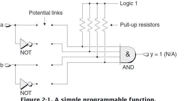
A simple programmable function
As a basis for these discussions, let’s start by considering a
very simple programmable function with two inputs calleda
andband a single outputy(Figure 2-1).
Fundamental Concepts
2
a
Logic 1
y = 1 (N/A) &
b
Pull-up resistors Potential links
NOT NOT
AND
The inverting (NOT) gates associated with the inputs mean that each input is available in both itstrue(unmodified) andcomplemented(inverted) form. Observe the locations of the potential links. In the absence of any of these links, all of the inputs to the AND gate are connected via pull-up resistors to a logic 1 value. In turn, this means that the outputywill always be driving a logic 1, which makes this circuit a very boring one in its current state. In order to make our function more interesting, we need some mechanism that allows us to establish one or more of the potential links.
Fusible link technologies
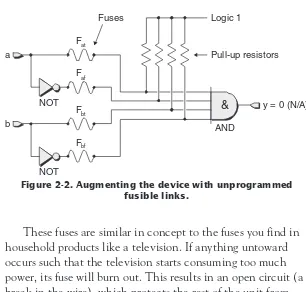
One of the first techniques that allowed users to program
their own devices was—and still is—known asfusible-link
technology. In this case, the device is manufactured with all of the links in place, where each link is referred to as afuse
(Figure 2-2).
These fuses are similar in concept to the fuses you find in household products like a television. If anything untoward occurs such that the television starts consuming too much power, its fuse will burn out. This results in an open circuit (a break in the wire), which protects the rest of the unit from
a
Fat
Logic 1
y = 0 (N/A) &
Faf
b
Fbt
Fbf
Pull-up resistors
NOT NOT
AND Fuses
Figure 2-2. Augmenting the device with unprogrammed fusible links.
25,000 BC:
harm. Of course, the fuses in a silicon chip are formed using the same processes that are employed to create the transistors and wires on the chip, so they are microscopically small.
When an engineer purchases a programmable device based on fusible links, all of the fuses are initially intact. This means that, in its unprogrammed state, the output from our example function will always be logic 0. (Any 0 presented to the input of an AND gate will cause its output to be 0, so if inputais 0, the output from the AND will be 0. Alternatively, if inputais 1, then the output from its NOT gate—which we shall call
!a—will be 0, and once again the output from the AND will
be 0. A similar situation occurs in the case of inputb.) The point is that design engineers can selectively remove undesired fuses by applying pulses of relatively high voltage and current to the device’s inputs. For example, consider what happens if we remove fusesFafandFbt(Figure 2-3).
Removing these fuses disconnects the complementary ver-sion of inputaand the true version of inputbfrom the AND gate (the pull-up resistors associated with these signals cause their associated inputs to the AND to be presented with logic 1 values). This leaves the device to perform its new function, which isy=a&!b. (The “&” character in this equation is
a
Fat
Logic 1
y = a & !b &
b
Fbf
Pull-up resistors
NOT NOT
AND
Figure 2-3. Programmed fusible links.
2,500 BC:
used to represent the AND, while the “!” character is used to represent the NOT. This syntax is discussed in a little more detail in chapter 3). This process of removing fuses is typically referred to asprogrammingthe device, but it may also be referred to asblowingthe fuses orburningthe device.
Devices based on fusible-link technologies are said to be
one-time programmable, or OTP, because once a fuse has been blown, it cannot be replaced and there’s no going back.
As fate would have it, although modern FPGAs are based on a wide variety of programming technologies, the fusible-link approach isn’t one of them. The reasons for mentioning it here are that it sets the scene for what is to come, and it’s rele-vant in the context of the precursor device technologies referenced in chapter 3.
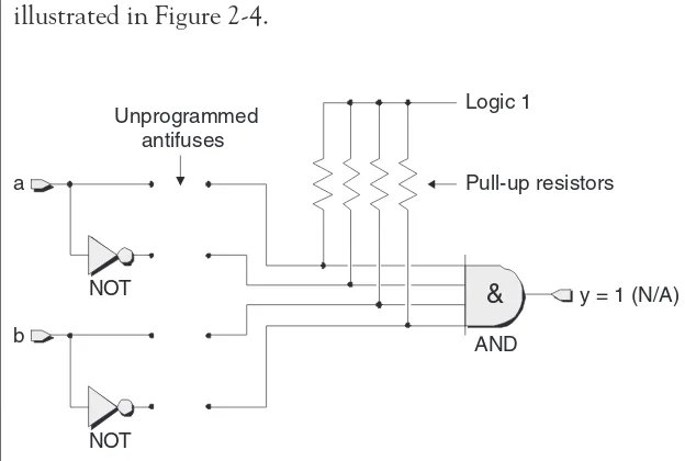
Antifuse technologies
As a diametric alternative to fusible-link technologies, we have their antifuse counterparts, in which each configurable path has an associated link called anantifuse. In its unpro-grammed state, an antifuse has such a high resistance that it may be considered an open circuit (a break in the wire), as illustrated in Figure 2-4.
OTP is pronounced by spelling it out as “O-T-P.”
a
Logic 1
y = 1 (N/A) &
b
Pull-up resistors Unprogrammed
antifuses
NOT NOT
AND
This is the way the device appears when it is first pur-chased. However, antifuses can be selectively “grown”
(programmed) by applying pulses of relatively high voltage and current to the device’s inputs. For example, if we add the anti-fuses associated with the complementary version of inputaand the true version of inputb, our device will now perform the functiony=!a&b(Figure 2-5).
An antifuse commences life as a microscopic column of amorphous (noncrystalline) silicon linking two metal tracks. In its unprogrammed state, the amorphous silicon acts as an insulator with a very high resistance in excess of one billion ohms (Figure 2-6a).
a
Logic 1
y = !a & b &
b
Pull-up resistors Programmed
antifuses
NOT NOT
AND
Figure 2-5. Programmed antifuse links.
Figure 2-6. Growing an antifuse.
260 BC:
The act of programming this particular element effectively
“grows” a link—known as avia—by converting the insulating
amorphous silicon into conducting polysilicon (Figure 2-6b). Not surprisingly, devices based on antifuse technologies are OTP, because once an antifuse has been grown, it cannot be removed, and there’s no changing your mind.
Mask-programmed devices
Before we proceed further, a little background may be advantageous in order to understand the basis for some of the nomenclature we’re about to run into. Electronic systems in general—and computers in particular—make use of two major
classes of memory devices:read-only memory (ROM)and
random-access memory (RAM).
ROMs are said to benonvolatilebecause their data remains when power is removed from the system. Other components in the system can read data from ROM devices, but they can-not write new data into them. By comparison, data can be both written into and read out of RAM devices, which are said to bevolatilebecause any data they contain is lost when the system is powered down.
Basic ROMs are also said to bemask-programmedbecause
any data they contain is hard-coded into them during their construction by means of the photo-masks that are used to create the transistors and the metal tracks (referred to as the
metallization layers) connecting them together on the silicon chip. For example, consider a transistor-based ROM cell that can hold a singlebitof data (Figure 2-7).
The entire ROM consists of a number ofrow(word) and
column(data) lines forming an array. Each column has a single pull-up resistor attempting to hold that column to a weak logic 1 value, and every row-column intersection has an asso-ciated transistor and, potentially, a mask-programmed
connection.
The majority of the ROM can be preconstructed, and the same underlying architecture can be used for multiple custom-ers. When it comes to customizing the device for use by a
ROM is pronounced to rhyme with “bomb.”
RAM is pronounced to rhyme with “ham.”
The concept of photo-masks and the way in which silicon chips are created are described in more detail inBebop to the Boolean Boogie (An Unconventional Guide to Electronics), ISBN 0-7506-7543-8
particular customer, a single photo-mask is used to define which cells are to include a mask-programmed connection and which cells are to be constructed without such a connection.
Now consider what happens when a row line is placed in its active state, thereby attempting to activate all of the tran-sistors connected to that row. In the case of a cell that includes a mask-programmed connection, activating that cell’s transis-tor will connect the column line through the transistransis-tor to logic 0, so the value appearing on that column as seen from the out-side world will be a 0. By comparison, in the case of a cell that doesn’t have a mask-programmed connection, that cell’s tran-sistor will have no effect, so the pull-up retran-sistor associated with that column will hold the column line at logic 1, which is the value that will be presented to the outside world.
PROMs
The problem with mask-programmed devices is that creat-ing them is a very expensive pastime unless you intend to produce them in extremely large quantities. Furthermore, such components are of little use in a development environment in which you often need to modify their contents.
For this reason, the firstprogrammable read-only memory (PROM)devices were developed at Harris Semiconductor in 1970. These devices were created using a nichrome-based
Tukey had initially con-sidered using “binit” or “bigit,” but thankfully he settled on “bit,” which is much easier to say and use.
The termsoftwareis also attributed to Tukey.
PROM is pronounced just like the high school dance of the same name. Logic 1
Pull-up resistor
Row (word) line
Column (data) line Mask-programmed
connection
Transistor
Logic 0
fusible-link technology. As a generic example, consider a somewhat simplified representation of a transistor-and-fusible-link–based PROM cell (Figure 2-8).
In its unprogrammed state as provided by the manufac-turer, all of the fusible links in the device are present. In this case, placing a row line in its active state will turn on all of the transistors connected to that row, thereby causing all of the column lines to be pulled down to logic 0 via their respec-tive transistors. As we previously discussed, however, design engineers can selectively remove undesired fuses by applying pulses of relatively high voltage and current to the device’s inputs. Wherever a fuse is removed, that cell will appear to contain a logic 1.
It’s important to note that these devices were initially intended for use as memories to store computer programs and constant data values (hence the “ROM” portion of their appellation). However, design engineers also found them use-ful for implementing simple logical functions such as lookup tables and state machines. The fact that PROMs were rela-tively cheap meant that these devices could be used to fix bugs or test new implementations by simply burning a new device and plugging it into the system.
Logic 1
Pull-up resistor
Row (word) line
Column (data) line Fusible link
Transistor
Logic 0
Figure 2-8. A transistor-and-fusible-link–based PROM cell. 15 BC:
Over time, a variety of more general-purpose PLDs based on fusible-link and antifuse technologies became available (these devices are introduced in more detail in chapter 3).
EPROM-based technologies
As was previously noted, devices based on fusible-link or antifuse technologies can only be programmed a single time—once you’ve blown (or grown) a fuse, it’s too late to change your mind. (In some cases, it’s possible to incremen-tally modify devices by blowing, or growing, additional fuses, but the fates have to be smiling in your direction.) For this rea-son, people started to think that it would be nice if there were some way to create devices that could be programmed, erased, and reprogrammed with new data.
One alternative is a technology known aserasable program-mable read-only memory (EPROM), with the first such
device—the 1702—being introduced by Intel in 1971. An EPROM transistor has the same basic structure as a standard MOS transistor, but with the addition of a second polysilicon
floating gateisolated by layers of oxide (Figure 2-9).
In its unprogrammed state, the floating gate is uncharged and doesn’t affect the normal operation of the control gate. In order to program the transistor, a relatively high voltage (the order of 12V) is applied between the control gate and drain
EPROM is pronounced by spelling out the “E” to rhyme with “bee,” followed by “PROM.”
(a) Standard MOS transistor (b) EPROM transistor
Silicon
terminals. This causes the transistor to be turned hard on, and energetic electrons force their way through the oxide into the floating gate in a process known ashot (high energy) elec-tron injection. When the programming signal is removed, a negative charge remains on the floating gate. This charge is very stable and will not dissipate for more than a decade under normal operating conditions. The stored charge on the float-ing gate inhibits the normal operation of the control gate and, thus, distinguishes those cells that have been pro-grammed from those that have not. This means we can use such a transistor to form a memory cell (Figure 2-10).
Observe that this cell no longer requires a fusible-link, antifuse, or mask-programmed connection. In its unpro-grammed state, as provided by the manufacturer, all of the floating gates in the EPROM transistors are uncharged. In this case, placing a row line in its active state will turn on all of the transistors connected to that row, thereby causing all of the column lines to be pulled down to logic 0 via their respec-tive transistors. In order to program the device, engineers can use the inputs to the device to charge the floating gates associ-ated with selected transistors, thereby disabling those
Logic 1
Pull-up resistor Row
(word) line
Column (data) line EPROM
Transistor
Logic 0
Figure 2-10. An EPROM transistor-based memory cell. 60 AD:
transistors. In these cases, the cells will appear to contain logic 1 values.
As they are an order of magnitude smaller than fusible links, EPROM cells are efficient in terms of silicon real estate. Their main claim to fame, however, is that they can be erased and reprogrammed. An EPROM cell is erased by discharging the electrons on that cell’s floating gate. The energy required to discharge the electrons is provided by a source ofultraviolet
(UV)radiation. An EPROM device is delivered in a ceramic
or plastic package with a small quartz window in the top, where this window is usually covered with a piece of opaque sticky tape. In order for the device to be erased, it is first removed from its host circuit board, its quartz window is uncovered, and it is placed in an enclosed container with an intense UV source.
The main problems with EPROM devices are their expen-sive packages with quartz windows and the time it takes to erase them, which is in the order of 20 minutes. A foreseeable problem with future devices is paradoxically related to
improvements in the process technologies that allow transis-tors to be made increasingly smaller. As the structures on the device become smaller and the density (number of transistors and interconnects) increases, a larger percentage of the surface of the die is covered by metal. This makes it difficult for the EPROM cells to absorb the UV light and increases the required exposure time.
Once again, these devices were initially intended for use as programmable memories (hence the “PROM” portion of their name). However, the same technology was later applied to more general-purpose PLDs, which therefore became known as
erasable PLDs (EPLDs).
EEPROM-based technologies
The next rung up the technology ladder appeared in the form ofelectrically erasable programmable read-only memories (EEPROMsorE2PROMs). An E2PROM cell is approximately 2.5 times larger than an equivalent EPROM cell because it
UV is pronounced by spelling it out as “U-V.”
EPLD is pronounced by spelling it out as “E-P-L-D.”
comprises two transistors and the space between them (Figure 2-11).
The E2PROM transistor is similar to that of an EPROM
transistor in that it contains a floating gate, but the insulating oxide layers surrounding this gate are very much thinner. The second transistor can be used to erase the cell electrically.
E2PROMs first saw the light of day as computer memories, but the same technology was subsequently applied to PLDs, which therefore became known aselectrically erasable PLDs (EEPLDsorE2PLDs).
FLASH-based technologies
A development known as FLASH can trace its ancestry to
both the EPROM and E2PROM technologies. The name
“FLASH” was originally coined to reflect this technology’s rapid erasure times compared to EPROM. Components based on FLASH can employ a variety of architectures. Some have a single floating gate transistor cell with the same area as an EPROM cell, but with the thinner oxide layers characteristic
of an E2PROM component. These devices can be electrically
erased, but only by clearing the whole device or large portions thereof. Other architectures feature a two-transistor cell simi-lar to that of an E2PROM cell, thereby allowing them to be erased and reprogrammed on a word-by-word basis.
In the case of the alterna-tive E2PROM designation, the “E2” stands for “E to the power of two,” or “E-squared.” Thus, E2PROM is pronounced “E-squared-PROM.”
EEPLD is pronounced by spelling it out as “E-E-P-L-D.”
E2PLD is pronounced “E-squared-P-L-D.”
E2PROM Cell
Normal MOS transistor
E2PROM transistor
Initial versions of FLASH could only store a single bit of data per cell. By 2002, however, technologists were experi-menting with a number of different ways of increasing this capacity. One technique involves storing distinct levels of charge in the FLASH transistor’s floating gate to represent two bits per cell. An alternative approach involves creating two discrete storage nodes in a layer below the gate, thereby sup-porting two bits per cell.
SRAM-based technologies
There are two main versions of semiconductor RAM
devices:dynamic RAM (DRAM)andstatic RAM (SRAM). In
the case of DRAMs, each cell is formed from a transistor-capacitor pair that consumes very little silicon real estate. The “dynamic” qualifier is used because the capacitor loses its charge over time, so each cell must be periodically recharged if it is to retain its data. This operation—known asrefreshing—is a tad complex and requires a substantial amount of additional circuitry. When the “cost” of this refresh circuitry is amortized over tens of millions of bits in a DRAM memory device, this approach becomes very cost effective. However, DRAM tech-nology is of little interest with regard to programmable logic.
By comparison, the “static” qualifier associated with SRAM is employed because—once a value has been loaded into an SRAM cell—it will remain unchanged unless it is spe-cifically altered or until power is removed from the system. Consider the symbol for an SRAM-based programmable cell (Figure 2-12).
DRAM is pronounced by spelling out the “D” to rhyme with “knee,” fol-lowed by “RAM” to rhyme with “spam.”
SRAM is pronounced by spelling out the “S” to rhyme with “less,” fol-lowed by “RAM” to rhyme with “Pam.”
SRAM
The entire cell comprises a multitransistor SRAM storage element whose output drives an additional control transistor. Depending on the contents of the storage element (logic 0 or logic 1), the control transistor will either be OFF (disabled) or ON (enabled).
One disadvantage of having a programmable device based on SRAM cells is that each cell consumes a significant amount of silicon real estate because these cells are formed from four or six transistors configured as a latch. Another dis-advantage is that the device’s configuration data (programmed state) will be lost when power is removed from the system. In turn, this means that these devices always have to be repro-grammed when the system is powered on. However, such devices have the corresponding advantage that they can be reprogrammed quickly and repeatedly as required.
The way in which these cells are used in SRAM-based FPGAs is discussed in more detail in the following chapters. For our purposes here, we need only note that such cells could conceptually be used to replace the fusible links in our exam-ple circuit shown in Figure 2-2, the antifuse links in Figure 2-4, or the transistor (and associated mask-programmed con-nection) associated with the ROM cell in Figure 2-7 (of course, this latter case, having an SRAM-based ROM, would be meaningless).
Summary
Table 2-1 shows the devices with which the various pro-gramming technologies are predominantly associated.
Additionally, we shouldn’t forget that new technologies are constantly bobbing to the surface. Some float around for a bit, and then sink without a trace while you aren’t looking; others thrust themselves onto center stage so rapidly that you aren’t quite sure where they came from.
For example, one technology that is currently attracting a great deal of interest for the near-term future ismagnetic RAM (MRAM). The seeds of this technology were sown back in
1974, when IBM developed a component called amagnetic
tunnel junction (MJT). This comprises a sandwich of two ferro-magnetic layers separated by a thin insulating layer. An MRAM memory cell can be created at the intersection of two tracks—say a row (word) line and a column (data) line—with an MJT sandwiched between them.
MRAM cells have the potential to combine the high speed of SRAM, the storage capacity of DRAM, and the
nonvolatility of FLASH, all while consuming a miniscule amount of power. MRAM-based memory chips are predicted to become available circa 2005. Once these memory chips do reach the market, other devices—such as MRAM-based FPGAs—will probably start to appear shortly thereafter.
Related technologies
In order to get a good feel for the way in which FPGAs developed and the reasons why they appeared on the scene in the first place, it’s advantageous to consider them in the con-text of other related technologies (Figure 3-1).
The white portions of the timeline bars in this illustration indicate that although early incarnations of these technologies may have been available, for one reason or another they wer-en’t enthusiastically received by the engineers working in the trenches during this period. For example, although Xilinx introduced the world’s first FPGA as early as 1984, design engineers didn’t really start using these little scamps with gusto and abandon until the early 1990s.
The Origin of FPGAs
3
1945 1950 1955 1960 1965 1970 1975 1980 1985 1990 1995 2000
FPGAs ASICs CPLDs SPLDs Microprocessors SRAMs & DRAMs ICs (General) Transistors
Transistors
On December 23, 1947, physicists William Shockley, Walter Brattain, and John Bardeen, working at Bell Laborato-ries in the United States, succeeded in creating the first transistor: a point-contact device formed from germanium (chemical symbol Ge).
The year 1950 saw the introduction of a more sophisti-cated component called abipolar junction transistor (BJT), which was easier and cheaper to build and had the added advantage of being more reliable. By the late 1950s, transistors were being manufactured out of silicon (chemical symbol Si) rather than germanium. Even though germanium offered cer-tain electrical advantages, silicon was cheaper and more amenable to work with.
If BJTs are connected together in a certain way, the result-ing digital logic gates are classed astransistor-transistor logic (TTL). An alternative method of connecting the same tran-sistors results inemitter-coupled logic (ECL). Logic gates constructed in TTL are fast and have strong drive capability, but they also consume a relatively large amount of power. Logic gates built in ECL are substantially faster than their TTL counterparts, but they consume correspondingly more power.
In 1962, Steven Hofstein and Fredric Heiman at the RCA research laboratory in Princeton, New Jersey, invented a new family of devices calledmetal-oxide semiconductor field-effect transistors (MOSFETs). These are often just called FETs for short. Although the original FETs were somewhat slower than their bipolar cousins, they were cheaper, smaller, and used substantially less power.
There are two main types of FETs, called NMOS and PMOS. Logic gates formed from NMOS and PMOS transis-tors connected together in a complementary manner are
known as acomplementary metal-oxide semiconductor (CMOS).
Logic gates implemented in CMOS used to be a tad slower than their TTL cousins, but both technologies are pretty
BJT is pronounced by spelling it out as “B-J-T.”
TTL is pronounced by spelling it out as “T-T-L.”
ECL is pronounced by spelling it out as “E-C-L.”
FET is pronounced to rhyme with “bet.”
much equivalent in this respect these days. However, CMOS logic gates have the advantage that their static (nonswitching) power consumption is extremely low.
Integrated circuits
The first transistors were provided as discrete components that were individually packaged in small metal cans. Over time, people started to think that it would be a good idea to fabricate entire circuits on a single piece of semiconductor. The first public discussion of this idea is credited to a British radar expert, G. W. A. Dummer, in a paper presented in 1952. But it was not until the summer of 1958 that Jack Kilby, work-ing forTexas Instruments (TI), succeeded in fabricating a phase-shift oscillator comprising five components on a single piece of semiconductor.
Around the same time that Kilby was working on his pro-totype, two of the founders of Fairchild Semiconductor—the Swiss physicist Jean Hoerni and the American physicist Robert Noyce—invented the underlying optical lithographic tech-niques that are now used to create transistors, insulating layers, and interconnections on modern ICs.
During the mid-1960s, TI introduced a large selection of basic building block ICs called the 54xx(“fifty-four hundred”) series and the 74xx(“seventy-four hundred”) series, which were specified for military and commercial use, respectively. These “jelly bean” devices, which were typically around 3/4" long, 3/8" wide, and had 14 or 16 pins, each contained small amounts of simple logic (for those readers of a pedantic dispo-sition, some were longer, wider, and had more pins). For example, a 7400 device contained four 2-input NAND gates, a 7402 contained four 2-input NOR gates, and a 7404 contained six NOT (inverter) gates.
TI’s 54xxand 74xxseries were implemented in TTL. By comparison, in 1968, RCA introduced a somewhat equivalent CMOS-based library of parts called the 4000 (“four thousand”) series.
SRAMs, DRAMs, and microprocessors
The late 1960s and early 1970s were rampant with new developments in the digital IC arena. In 1970, for example, Intel announced the first 1024-bit DRAM (the 1103) and Fairchild introduced the first 256-bit SRAM (the 4100).
One year later, in 1971, Intel introduced the world’s first
microprocessor (µP)—the 4004—which was conceived and created by Marcian “Ted” Hoff, Stan Mazor, and Federico Faggin. Also referred to as a “computer-on-a-chip,” the 4004 contained only around 2,300 transistors and could execute 60,000 operations per second.
Actually, although the 4004 is widely documented as being the first microprocessor, there were other contenders. In February 1968, for example, International Research Corpora-tion developed an architecture for what they referred to as a
“computer-on-a-chip.”And in December 1970, a year before the 4004 saw the light of day, one Gilbert Hyatt filed an application for a patent entitled“Single Chip Integrated Circuit Computer Architecture”(wrangling about this patent continues to this day). What typically isn’t disputed, however, is the fact that the 4004 was the first microprocessor to be physically constructed, to be commercially available, and to actually per-form some useful tasks.
The reason SRAM and microprocessor technologies are of interest to us here is that the majority of today’s FPGAs are SRAM-based, and some of today’s high-end devices incorpo-rate embedded microprocessor cores (both of these topics are discussed in more detail in chapter 4).
SPLDs and CPLDs
The first programmable ICs were generically referred to as
programmable logic devices (PLDs). The original components, which started arriving on the scene in 1970 in the form of PROMs, were rather simple, but everyone was too polite to mention it. It was only toward the end of the 1970s that sig-nificantly more complex versions became available. In order
SRAMand DRAMare pro-nounced by spelling out the “S” or “D” to rhyme with “mess” or “bee,” respectively, followed by “RAM” to rhyme with “spam.”
to distinguish them from their less-sophisticated ancestors, which still find use to this day, these new devices were referred to ascomplex PLDs (CPLDs). Perhaps not surprisingly, it subse-quently became common practice to refer to the original, less-pretentious versions assimple PLDs (SPLDs).
Just to make life more confusing, some people understand the terms PLD and SPLD to be synonymous, while others regard PLD as being a superset that encompasses both SPLDs and CPLDs (unless otherwise noted, we shall embrace this lat-ter inlat-terpretation).
And life just keeps on getting better and better because engineers love to use the same acronym to mean different things or different acronyms to mean the same thing (listening to a gaggle of engineers regaling each other in conversation can make even the strongest mind start to “throw a wobbly”). In the case of SPLDs, for example, there is a multiplicity of underlying architectures, many of which have acronyms formed from different combinations of the same three or four letters (Figure 3-2).
Of course there are also EPLD, E2PLD, and FLASH
ver-sions of many of these devices—for example, EPROMs and
E2PROMs—but these are omitted from figure 3-2 for purposes
of simplicity (these concepts were introduced in chapter 2).
PLDs
SPLDs CPLDs
PLAs
PROMs PALs GALs etc.
Figure 3-2. A positive plethora of PLDs.
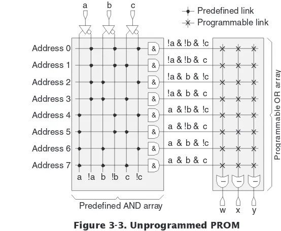
PROMs
The first of the simple PLDs were PROMs, which appeared on the scene in 1970. One way to visualize how these devices perform their magic is to consider them as con-sisting of a fixed array of AND functions driving a
programmable array of OR functions. For example, consider a 3-input, 3-output PROM (Figure 3-3).
The programmable links in the OR array can be
imple-mented as fusible links, or as EPROM transistors and E2PROM
cells in the case of EPROM and E2PROM devices,
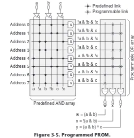
respec-tively. It is important to realize that this illustration is intended only to provide a high-level view of the way in which our example device works—it does not represent an actual circuit diagram. In reality, each AND function in the AND array has three inputs provided by the appropriate true or complemented versions of thea,b, andcdevice inputs. Similarly, each OR function in the OR array has eight inputs provided by the outputs from the AND array.
PROMis pronounced like the high school dance of the same name.
Figure 3-3. Unprogrammed PROM
As was previously noted, PROMs were originally intended for use as computer memories in which to store program instructions and constant data values. However, design engi-neers also used them to implement simple logical functions such as lookup tables and state machines. In fact, a PROM can be used to implement any block of combinational (or combi-national) logic so long as it doesn’t have too many inputs or outputs. The simple 3-input, 3-output PROM shown in Figure 3-3, for example, can be used to implement any combinatorial function with up to 3 inputs and 3 outputs. In order to under-stand how this works, consider the small block of logic shown in Figure 3-4 (this circuit has no significance beyond the pur-poses of this example).
We could replace this block of logic with our 3-input, 3-output PROM. We would only need to program the appro-priate links in the OR array (Figure 3-5).
With regard to the equations shown in this figure, “&” rep-resents AND, “|” reprep-resents OR, “^” reprep-resents XOR, and “!” represents NOT. This syntax (or numerous variations thereof) was very common in the early days of PLDs because it allowed logical equations to be easily and concisely represented in text files using standard computer keyboard characters.
The above example is, of course, very simple. Real PROMs can have significantly more inputs and outputs and can, there-fore, be used to implement larger blocks of combinational logic. From the mid-1960s until the mid-1980s (or later),
Some folks prefer to say “combinational logic,” while others favor “com-binatorial logic.”
The ‘&’ (ampersand) char-acter is commonly referred to as an “amp” or “amper.”
The ‘|’ (vertical line) char-acter is commonly referred to as a “bar,” “or,” or “pipe.”
combinational logic was commonly implemented by means of jelly bean ICs such as the TI 74xxseries devices.
The fact that quite a large number of these jelly bean chips could be replaced with a single PROM resulted in cir-cuit boards that were smaller, lighter, cheaper, and less prone to error (each solder joint on a circuit board provides a poten-tial failure mechanism). Furthermore, if any logic errors were subsequently discovered in this portion of the design (if the design engineer had inadvertently used an AND function instead of a NAND, for example), then these slipups could easily be fixed by blowing a new PROM (or erasing and
repro-gramming an EPROM or E2PROM). This was preferable to
the ways in which errors had to be addressed on boards based on jelly bean ICs. These included adding new devices to the board, cutting existing tracks with a scalpel, and adding wires by hand to connect the new devices into the rest of the circuit.
The ‘^’ (circumflex) char-acter is commonly referred to as a “hat,” “control,” “up-arrow,” or “caret.” More rarely it may be referred to as a “chevron,” “power of” (as in “to the power of”), or “shark-fin.”
The ‘!’ (exclamation mark) character is com-monly referred to as a “bang,” “ping,” or
In logical terms, the AND (“&”) operator is known as a
logical multiplicationorproduct, while the OR (“|”) operator is known as alogical additionorsum. Furthermore, when we have a logical equation in the form
y= (a&!b&c) | (!a&b&c) | (a&!b&!c) | (a&!b&c)
then the termliteralrefers to any true or inverted variable (a,
!a,b,!b, etc.), and a group of literals linked by “&” operators is referred to as aproduct term. Thus, the product term (a&!b&
c) contains three literals—a,!b, andc—and the above equa-tion is said to be insum-of-productsform.
The point is that, when they are employed to implement combinational logic as illustrated in figures 3-4 and 3-5, PROMs are useful for equations requiring a large number of product terms, but they can support relatively few inputs because every input combination is always decoded and used.
PLAs
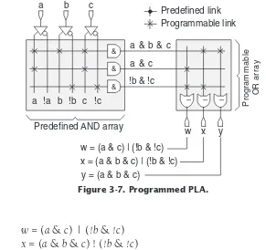
In order to address the limitations imposed by the PROM architecture, the next step up the PLD evolutionary ladder was that ofprogrammable logic arrays (PLAs), which first became available circa 1975. These were the most user configurable of the simple PLDs because both the AND and OR arrays were programmable. First, consider a simple 3-input, 3-output PLA in its unprogrammed state (Figure 3.6).
Unlike a PROM, the number of AND functions in the AND array is independent of the number of inputs to the device. Additional ANDs can be formed by simply introducing more rows into the array.
Similarly, the number of OR functions in the OR array is independent of both the number of inputs to the device and the number of AND functions in the AND array. Additional ORs can be formed by simply introducing more columns into the array.
Now assume that we wish our example PLA to implement the three equations shown below. We can achieve this by pro-gramming the appropriate links as illustrated in Figure 3-7.
w= (a&c) | (!b&!c)
Figure 3-6. Unprogrammed PLA (programmable AND and OR arrays).
a b c
Figure 3-7. Programmed PLA. 1600:
As fate would have it, PLAs never achieved any significant level of market presence, but several vendors experimented with different flavors of these devices for a while. For example, PLAs were not obliged to have AND arrays feeding OR arrays, and some alternative architectures such as AND arrays feeding NOR arrays were occasionally seen strutting their stuff. How-ever, while it would be theoretically possible to field
architectures such as OR-AND, NAND-OR, and
NAND-NOR, these variations were relatively rare or
nonex-istent. One reason these devices tended to stick to AND-OR1
(and AND-NOR) architectures was that the sum-of-products representations most often used to specify logical equations could be directly mapped onto these structures. Other equa-tion formats—like product-of-sums—could be accommodated using standard algebraic techniques (this was typically per-formed by means of software programs that could perform these techniques with their metaphorical hands tied behind their backs).
PLAs were touted as being particularly useful for large designs whose logical equations featured a lot of common product terms that could be used by multiple outputs; for example, the product term (!b&!c) is used by both thewand
xoutputs in Figure 3-7. This feature may be referred to as
product-term sharing.
On the downside, signals take a relatively long time to pass through programmable links as opposed to their predefined counterparts. Thus, the fact that both their AND and OR arrays were programmable meant that PLAs were significantly slower than PROMs.
1Actually, one designer I talked to a few moments before penning these words told me that his team created a NOT-NOR-NOR-NOT
architecture (this apparently offered a slight speed advantage), but they told their customers it was an AND-OR architecture (which is how it appeared to the outside world) because “that was what they were
expecting.” Even today, what device vendors say they build and what they actually build are not necessarily the same thing.
1614: