Development of Neuromorphic SIFT Operator with Application to High Speed Image
Matching
M. Shankayi a*, M. Saadatseresht a, M. A.V. Bitetto b
a University of Tehran, Geomatics Engineering Faculty, Tehran, Iran - (mshankayi, msaadat)@ut.ac.ir
b Institute of Cybernetics Research, Inc. , Robotics and Control Systems Department, New York, USA – [email protected]
KEY WORDS: Neuromorphics, SIFT, Image Matching, FPGA, Neural Network
ABSTRACT:
There was always a speed/accuracy challenge in photogrammetric mapping process, including feature detection and matching. Most of the researches have improved algorithm's speed with simplifications or software modifications which increase the accuracy of the image matching process. This research tries to improve speed without enhancing the accuracy of the same algorithm using Neuromorphic techniques.In this research we have developed a general design of a Neuromorphic ASIC to handle algorithms such as SIFT. We also have investigated neural assignment in each step ofthe SIFT algorithm. With a rough estimation based on delay of the used elements including MAC and comparator, we have estimated the resulting chip's performance for 3 scenarios, Full HD movie (Videogrammetry), 24 MP (UAV photogrammetry), and 88 MP image sequence. Our estimations led to approximate 3000 fps for Full HD movie, 250 fps for 24 MP image sequence and 68 fps for 88MP Ultracam image sequence which can be a huge improvement for current photogrammetric processing systems. We also estimated the power consumption of less than10 watts which is not comparable to current workflows.
1. INTRODUCTION
Neuromorphic techniques include both electronic and bio-inspired studies which enables the user to reach a much higher performance per watt in the compatible algorithms. Several companies such as Intel, Qualcomm and IBM are currently developing Neuromorphic chips so that the developers will be able to use the neural architecture in many studies. This improvement demands a significant change in algorithm's processing architecture. The resulting architecture can be implemented using customized CMOS chips. However, it also can be simulated using FPGA elements to define each neural unit and produce an equivalent to that CMOS chip with a lower speed. The Neuromorphic framework in this research is not restricted to SIFT operator, and can be used dynamically to compute any other mathematical operator, from comparison based (binary) operators like FREAK to bio inspired object recognition methods such as HMAX. Generally this method is based on neural units as computational elements used for operations such as averaging, Gaussian or comparison. The entire process is based on logic gates which are packed into a neural unit. There are four types of neural units which are developed using CMOS library which can be simulated with FPGAs. Based on the input data, image sequence vs. high resolution images, assignment of these neural units may vary to reach the maximum throughput.
However this research attempts to purely speed up the algorithm but it's also presenting a scalable framework for SIFT operator to reach very high frames per second, since there is no delay in the processor for analysing input commands. This will results in several thousands of frames per second. This estimation is based on a computationally equivalent algorithm on CM1K Application Specific Integrated Circuit (ASIC) package which is reached to 500 nano-seconds delay. The resulting algorithm can be used on a customized ASIC package as a co-processor in any computational scale.
In the first look, a several thousand frames per second is not needed for many applications, but this huge improvement in performance results in much lower power consumption in 30-60 fps range. Lowering the power consumption of the device can be useful in devices such as smart glasses, smartphones, security cameras and smart cars. Lowering the power consumption leads
to low temperature, passive cooling and smaller package size of the computational unit.
Development of such ASIC packages demands a great use of electronics which is not the main goal of this research, subsequently a mid-range FPGA is used to simulate the ASIC chip in SIFT computations which lowers the target FPS to several hundreds. There test images include 24 MP aerial images and HD close range image sequence. The processing time is then compared to several commercial photogrammetry softwares such as AGISoft to show the applicability of the research.
2. LITERATURE REVIEW
In this section, FPGA and ASIC applications in image processing are explained and some of commercial devices are mentioned. Then the FPGA implementation of SIFT and some of optimizations by other researchers are briefly described.
2.1 ASIC and FPGAs for image processing
Since an FPGA implements the logic required by an application by building separate hardware for each function, FPGAs are inherently parallel. This gives them the speed that results from a hardware design while retaining the reprogrammable flexibility of software at a relatively low cost. This makes FPGAs well suited to image processing, particularly at the low and intermediate levels where they are able to exploit the parallelism inherent in images.
Nowadays this type of processing is found in many security, traffic and professional cameras, in which an FPGA is coupled to the CMOS directly. Altera Cyclone, Xilinx and Lattice are the most used FPGA brands in these cameras.
ASICs are a little different than FPGA since they are optimized for a specific application, which leads to a more costly solution as well as a higher speed. An FPGA requires 20–40 times the silicon area of an equivalent ASIC but it is cheaper due to its added value in higher volumes of production. On the other hand, ASICs are much faster than equivalent FPGAs, consume less power and are smaller so that the form factor will be completely different. An example of ASICs are image processors such as
BIONZ in Sony, DIGIC in canon and EXPEED in Nikon cameras.
There are ASICs used in other fields than RAW image processing such as CM1K in neural network development field also. Metaio also had an ASIC under development in order to handle Augmented Reality applications in image and location processing algorithms in the past years.
2.2 FPGA SIFT
There were many efforts in SIFT parallelization including [4 - 9] each of which have improved the algorithms performance by implementing it on a FPGA device. [10] used five element Gaussian filters and four iterations of CORDIC1 to calculate the magnitude and direction of the gradient. They also simplified the gradient calculation, with only one filter used per octave rather than one per scale. [11] made the observation that after down-sampling the data volume is reduced by a factor of four. This allows all of the processing for the second octave and below to share a single Gaussian filter block and peak detect block. [12] took the processing one step further and also implemented the descriptor extraction in hardware. The gradient magnitude used the simplified formulation of eq. 1 rather than the square root, and a small lookup table was used to calculate the orientation. They used a modified descriptor that had fewer parameters, but was easier to implement in hardware. The feature matching, however, was performed in software using an embedded MicroBlaze processor.
� = |�| + |�| ��.
3. PROPOSED METHOD
In this section we’re going to describe the proposed method in detail including neural assignment, network size and reusability of the neurons.
3.1 Neuron Types
There are 5 types of electronic neurons defined in this network, each of which are capable of forming an independent part of network which can be used by specific functions of SIFT computation. The most important elements in any photogrammetric computation is multiplication as well as accumulation. So, there are two types of electronic neurons for multiplication and accumulation in this network which are called N1 and N2 respectively. The third neural element is one of the most famous hardware elements in the past decade called MAC which is composed by combining several multiplication units with an accumulation unit. We have used a very fast implementation of MAC, [1], in our NP1 neural element. The fourth and fifth types of electronic neurons are not arithmetic functions, instead, they solve logical problems. N3 neural unit is a logical element and it can act as any logical gate including NAND, NOR, XOR … only by changing its inputs. N3 neural unit is also capable of producing constant true or false outputs independent of its main inputs. It will be used to adapt the neural network to algorithms other than SIFT which are not the subject of this paper.
There is a need to comparators in any type of photogrammetric problems which are concerned about any type of thresholding. So, the last type of electronic neurons, so called N4 in this paper, is a 16-bit comparator which can be used in neighbourhood comparison in SIFT as well as any comparison operation in other algorithms such as FREAK. In the following sections the
1 Coordinate Rotation Digital Computer, an iterative technique for evaluating elementary functions. [3]
architectures of NP1-N4 and their input and output formats and measured delay are described.
3.1.1 Multiply and Accumulator Architecture (NP1)
NP1 contains the most important element in every photogrammetric calculation, including collinearity equations, fundamental matrix calculation, and descriptor generation. It’s originally a MAC unit which is developed by [1] and has eight inputs of 16 bit floating numbers. In order to fit the Gaussian kernel we’ll modify this unit to have ten inputs, which fits the five kernel size. It also generates one 16-bit output which is computed as fig. 1.
Figure 1. MAC architecture
This unit contains two sub units, N1 and N2. N1 is a multiplication unit which handles four parallel 16-bit multiplication operations. The N2 unit handles the summation of N1’s five outputs and have one 16-bit output.
Computation delay of NP1, N1 and N2 are shown in table 1 with respect to the original eight input MAC developed in [1].
Table 1. NP1 neuron, MAC specifications
Multiplication Accumulation MAC Delay
(ns)
1.312 1.247 1.692
Power (mw)
- - 8.2
Area (µ� )
- - 12014
3.1.2 Comparator Architecture (N4)
N4 Comparator unit plays an important role in every thresholding operation. We have used an implementation in [2] for N4 16-bit comparator unit. Its architecture has been shown in fig. 3.
Figure 2. Comparator Architecture
Specifications of 64-bit and 16-bit comparators used in N4 neural unit are shown in table 2.
Table 2. N4 neuron, Comparator specifications
64 bit comparator 16 bit comparator
Delay (ns) 0.86 ~0.62
Power (mw)
7.76 ~2
Transistor count
4000 ~1000
3.2 Gaussian Convolution
Any convolution algorithm consists of several Multiplication and Accumulation (MAC) operations, so the first section of our proposed neural network will be the network of NP1 neural elements. In order to increase usability of this section each NP1 is divided to N1 and N2 neural units so that the multiplication and accumulation parts can be used separately.
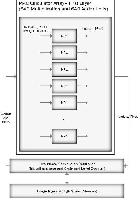
It's obvious that the size of NP1 network is highly dependent of its compatibility to image resolutions such as HD, full HD and so on. In the other hand, there are two limitations due to production and speed aspects of this problem. The production limitation is about the maximum number of transistors in a single chip, which limits the size of our computational network. The speed limitation concerns about number of computation cycles for total pixels in a single image. If the size of NP1 network is to small it will be needed to handle a single computation for too many cycles so that the total speed of entire chip will decrease. On the other hand, the exact assignment of each neural unit should be specified before determining the optimal size for computational networks. A convolution operation is dependent of the kernel size as well as the size of the image, in this case on of the image dimensions should be multiplication of number of the neurons in this network. To make it simple, we embedded the kernel size in each neural element. Due to the 5 x 5 kernel size each NP1 neuron should be able to handle 5 MACs in each cycle so that each NP1 neuron will have 10 inputs (5 pixels and 5 weights) and one output. Assuming HD or full HD size of the input frame, the number of NP1 neurons should be the maximum number that can be multiplied to 1280 or 1920 which leads to 640
NP1 neurons. Using 640 NP1 neurons with a 5*5 separable Gaussian kernel, leads to 2*720*2 or 3*1080*2 cycles of computation for an HD or full HD image respectively. The last 2 stands for 2 phases of convolution due to separate horizontal and vertical Gaussian kernel. Both kernel weights and pixel values for each level of image pyramid are stored in high speed memory, which can be either common DDR3 memory or the HBM type memory which is used in newly produced GPUs.
Two Phase Convolution Controller (including phase and Cycle and Level Counter)
NP1
NP1
NP1
NP1
NP1
:
NP1
10-inputs (16-bit)
5 weights, 5 pixels 1-output (16-bit)
Weights and Pixels
Updated Pixels
Image Pyramid(High Speed Memory)
Figure 3. Neuromorphic layout for Gaussian Convolution Phase
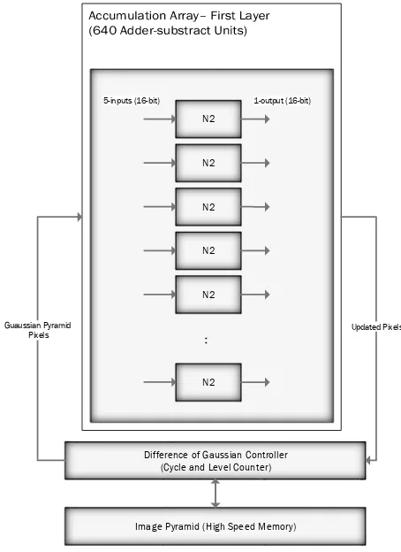
3.3 Difference of Gaussians
It is obvious that same window can't be used to detect key-points with different scale. It is possible with small corner but to detect larger corners larger windows are needed. Scale-space filtering is used to solve this. Laplacian of Gaussian is found for the image with various σ values in the scale-space filtering process. LoG acts as a blob detector which detects blobs in various sizes due to change in σ. In other words, σ acts as a scaling parameter. For e.g., in the above image, Gaussian kernel with low σ gives high value for small corner while Gaussian kernel with high σ fits well for larger corner. So, we can find the local maxima across the scale and space which gives us a list of (x,y,σ) values which means there is a potential key-point at (x,y) at σ scale.
SIFT algorithm uses Difference of Gaussians which is an approximation of LoG. Difference of Gaussian is obtained as the difference of Gaussian blurring of an image with two different σ, let it be σ and kσ. This process is done for different octaves of the image in Gaussian Pyramid. Which is shown in figure…
Figure 4. Difference of Gaussians
After Computation of Gaussian in each octave, the difference operation can be done by using the same array of adders (640 N2 units) in NP1 network. We’ve used the adder architecture described in [1] because of its simple of implementation and high speed.
Difference of Gaussian Controller (Cycle and Level Counter)
N2
N2
N2
N2
N2
:
N2
5-inputs (16-bit) 1-output (16-bit)
Guaussian Pyramid Pixels
Updated Pixels
Image Pyramid (High Speed Memory)
Figure 5. Neuromorphic layout for Difference of Gaussians
3.4 Comparison
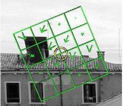
Once this DoG are found, images are searched for local extrema over scale and space. For e.g., one pixel in an image is compared with its 8 neighbours as well as 9 pixels in next scale and 9 pixels in previous scales. If it is a local extrema, it is a potential key-point. It basically means that key-point is best represented in that scale which is shown in figure 6 and 7.
Figure 6. Scale space extrema comparison
Neighborhood Comparison Controller (Cycle Counter)
N4
N4
N4
N4
N4
:
N4
2-inputs (16-bit) 1-output (2-bit)
Neighbor Pixels 2-bit array
Image Pyramid(High Speed Memory)
Figure 7. Neuromorphic layout for Neighbourhood Comparison
3.5 Fine Scale Calculation
Once potential key-points locations are found, they have to be refined to get more accurate results. They used Taylor series expansion of scale space to get more accurate location of extrema, and if the intensity at this extrema is less than a threshold value, it is rejected.
DoG has higher response for edges, so edges also need to be removed. A concept similar to Harris corner detector is used for edge removal. So that, a 2x2 Hessian matrix (H) is used to compute the principal curvature and if the ratio of eigen values is greater than a threshold, so called edge threshold, that key-point is discarded. Using the edge threshold will eliminate any low-contrast key-points and edge key-points and what remains is strong interest points.
3.6 Orientation Assignment
In the SIFT operator, an orientation is assigned to each key-point to achieve invariance to image rotation. A neighbourhood is taken around the key-point location depending on the scale, and the gradient magnitude and direction is calculated in that region. An orientation histogram with 36 bins covering 360 degrees is created. (It is weighted by gradient magnitude and Gaussian-weighted circular window with σ equal to 1.5 times the scale of key-point. The highest peak in the histogram is taken and any peak above 80% of it is also considered to calculate the orientation. It creates key-points with same location and scale, but different directions. It contribute to stability of matching.
Figure 8. Orientation assignment
3.6.1 Tangent Approximation
Despite of any advantages in ASIC compatible algorithms, there’s always a limitation of using complex functions such as trigonometric operations. As it’s obvious, rotation assignment and descriptor generation parts of SIFT algorithm both need to compute inverse tangent of the horizontal to vertical gradient ratio which cannot be done directly. Fortunately, many functions have been approximated in embedded computing applications including the inverse tangent.
There are several types of approximation with different accuracies and speeds. We have used the table 3 because of its simplicity, accuracy of 0.3 degrees and MAC compatibility. The detail of inverse tangent approximation is shown in table 3.
Table 3. Approximate equation (radians) for tan
Octant Radians computation due to formula (). After that, the N1 neurons will do
the dividing operation in formula () to finish the inverse tangent computation.
In order to generate the orientation histogram, N4 neurons needed for comparison and categorization of computer orientations into 32 bins each of which will cover 11.25 degrees in 360. Decreasing the number of bins in the orientation histogram leads to better compatibility of network size and also it’s recommended because of inverse tangent approximation. However, it could decreased to 16 bins to lower the orientation noise due to 0.3 degrees accuracy, while it was also unknown in the robustness aspect of SIFT operator. Decreasing 36 bins to 32 also improve the performance by reducing computation cycles by 12.5 %.
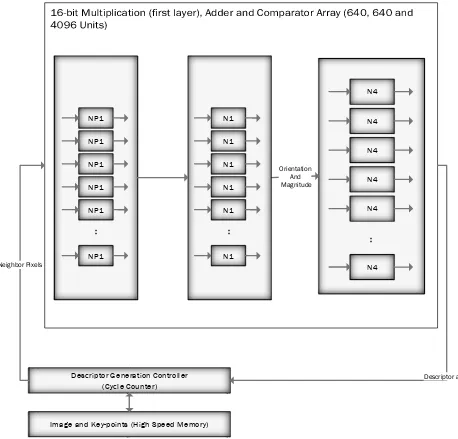
3.7 Descriptor Generation
The descriptor generation controller acts exactly like orientation assignment section by doing the same computations in a 16*16 neighbourhood containing 4*4 sub-blocks. For each sub-block, 8 bin orientation histogram is created. So a total of 128 bin values are available. It is represented as a vector to form key-point descriptor. In addition to this, several measures are taken to achieve robustness against illumination changes, rotation etc.
3.8 Performance Evaluation
In this section, an overview of estimated performance, power consumption and area of the resulting chip layout is described. According to reusability of two layer MAC architecture as well as comparator neural units, there is a maximum number of 640 MAC units in the first layer, 128 MAC units in the second layer and 4096 comparator units which will be used by controllers of each phase of the algorithm. The transistor count, power consumption and area of each controller is currently unknown but it will be much less than the entire neural units described here.
3.8.1 Gaussian Convolution
Having 3*1080*2 cycles of computation leads to 10 microseconds of delay due to 1.6 ns delay of each NP1 (MAC) neuron. However, this delay should multiplied by 6.6, which is the number of total octaves and scales (4 and 5 respectively), gives about 66 microseconds of delay. Since each octave halves the image dimension, the total processing time consumed for all octaves should be +4+ 6+64= . 8 5 which multiplies by the number of scale levels in each octave and gives slow down factor of about 6.6. According to the fact that this stage processes the massive number of pixels in high number of scale levels, it can be said that it will be the slowest part of the algorithm. On the other hand, this stage will not consume the highest power since it doesn’t use N4 neurons. The entire power consumption of this stage should be about 5 watt.
3.8.2 Difference of Gaussians
In order to calculate the number of processing cycles for total difference operations, assuming a full HD image, 4 octaves and 5 scales, we will have total number of pixels in each octave, 2 million, 500k, 125k and 31250. Assuming 4 subtraction operations in each octave leads to total number of pixels processed in each octave, 8 million, 2 million, 500k, and 125k. So the Total number of pixels processed in all octaves will be 10625000. Having 640 NP1 neurons leads to about 16600 cycles. If we use N2 array to subtract two images, it gives about 1.2 ns of delay in each operation, which will produce about 19 microseconds of delay. Using NP1 neurons will increase this delay to about 26 microseconds. So the entire DoG delay will be 92 microseconds.
3.8.3 Comparison
Assuming 3 scale levels in each octave, there are 26*3* total number of pixels in each scale level in each octave, leads to about 207 millions of comparison operations. Having 4096 enables the chip to process about 157*26 comparison operations in each cycle. This leads to 50757 cycles of comparison and produces about 31 microseconds of delay. It will consume 8 watts of power since almost all of N4 neurons are active.
3.8.4 Orientation Assignment
One of the main power consumption bottle necks lies in orientation assignment and descriptor generation steps, which use both NP1 and N4 neurons simultaneously. However they will operate at very high speeds of processing since assuming 10k key-points versus 2 million pixels, gives a huge difference in processing cycles. Assuming 32 bins of histogram, a 4*4 neighbourhood, and 8 directional gradients, leads to total number of 128 MACs of first layer, 32 MACs of the second layer and 32 comparisons in each cycle for each key-point. Having 512 and 128 MACs in two layers, limits the chip to process only 4 cycles simultaneously. The first layer of NP1 neurons will calculate 64 MAC operations for total 16 pixels in 2 direction each of which contain 2 MAC operations to calculate the gradient. Then the first layer of NP1 neurons do the 4 operations including AB, A^2, B^2 and base angle (depending on the octant) which use all 512 NP1 neurons in the first layer for 8 key-points in each cycle (16 pixels and 2 directions, 4 calculations). Then the second layer calculates
. 8 5 multiplication into A^2 or B^2 depending on the octant which uses all 128 NP1 neurons in the second layer for 8 key-points. Then the divide operation will be calculated using the second layer N1 neurons (in NP1 neurons). After this step, the N4 neurons are responsible to categorize the output orientation angle into the bins of orientation histogram. So there are 32 bins for each point and 32 N4 neurons are used for each key-point. Having 4096 N4 neurons leads to 128 key-point in each cycle. Assuming 10k key-points in each image it leads to 7.5k cycles for NP1 neurons and about 80 cycles for 10k key-points. This leads to maximum delay of 12 microseconds for NP1 neurons and 49.6 nanoseconds for N4 neural units. Due to huge cycle difference between NP1 and N4 neurons the power consumption of this stage will not be much higher than the NP1 neurons themselves leading to 5-6 watts.
3.8.5 Descriptor Generation
In order to calculate power consumption and delay of this we have to calculate just to scale factors for NP1 and N4 neurons. NP1 neurons should calculate 16 times more than the orientation assignment process since there are 16 of these 4*4 neighbourhoods in each key-point. On the other hand N4 neurons are 4 times less engaged with respect to orientation assignment section since orientation histogram is 8-bin instead of 32-bin. Due to low number of cycles of N4 neurons they will have almost no effect in delay because of their approximately 20 cycles while NP1 neurons slow down the entire process of MAC calculation by 1/16 scale factor which leads to 192 microseconds. As it’s obvious since we used the same NP1 and N4 arrays in multiple processes we faced a slowdown in comparison section for low number of N4 neurons while the exact number of N4 neurons were too much for orientation assignment and descriptor generation
3.8.6 Resulting frame rate
As the delay and power consumption of the resulting chip has been estimated in previous sections it will operate approximately in the range of 2000-3000 frames per second (327 micro seconds delay) of Full HD movie which is absolutely different from current photogrammetric processes.
3.8.7 High resolution Image Sequence
Since, all of evaluations in the previous sections were related to videogrammetry, with the assumption of Full HD video input, we're going to evaluate the resulting chip's performance on 24 and 88 (Ultracam) megapixels image input which is very common in UAV and traditional photogrammetry.
Assuming the number of key-points to resolution ratio is constant, the 327 µs delay will be about 4000 µs which leads to about 250 frames per second for 24 MP input. For Ultracam images, it should take about 14 ms to detect key-points and calculate descriptors in 88 MP which is equivalent to 68 frames per second.
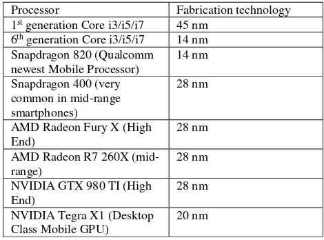
However, all of these numbers, are dependent on fabrication technology, which changes power consumption and speed. Due to the fact that NP1 and N4 neurons use a MAC implementation which is based on 150nm and 65nm technology respectively. Just for a comparison, table 4 shows some of the common processors with their fabrication technology.
Table 4. Some common processors with their fabrication
AMD Radeon Fury X (High End)
28 nm
AMD Radeon R7 260X (mid-range)
28 nm
NVIDIA GTX 980 TI (High End)
As it mentioned before, area of each NP1 neuron (MAC) is equal to 12000 µm^2 with 0.15 micron fabrication technology. Area of each N4 neuron also can be computed using a rough estimation with respect to a regular Core 2 Duo CPU with 291 million transistors and 143 mm^2 die size or 8800GT GPU with 754 million transistors and 324 mm^2 die size. Each N4 neuron consists of approximately 1000 transistors which is equal to 429 µm^2. Having 640 NP1 and 4096 N4 neurons leads to an approximate die size of 10 mm^2 with 0.15 and 0.065 micron fabrication technology for NP1 and N4 neurons respectively. By upgrading the fabrication technology for all neurons to 28nm the chip will be significantly smaller.
3.9 Future Works
This papers is just a part from a bigger research named “Design of a Reconfigurable Neuromorphic Framework for Photogrammetric applications” which is PhD thesis of the author. There are several sections concerning about other algorithms like HMAX, FREAK, 2.5D and 3D SIFT which are all compatible to this type of computation. The resulting chip should be able to handle any similar algorithm at very high speeds or very low power consumptions.
One of the other suggestions for continuing this line of research is to port photogrammetric equations, matching problem, classifiers and filtering algorithms to these neural elements which leads to change of the chip layout in network size and neural element aspects.
There is another idea in these type of neural networks which concerns about learning algorithm, which can enable each neural element (consisting these basic elements such as N1, N2) to learn how to act in every algorithm.
3.10Conclusion
In this research, an implementation of Neuromorphic SIFT for ASICs is described. The main difference of this method with the others is the ability to adapt to other algorithms such as HMAX and FREAK without major change in chip’s layout. This method can be used in any photogrammetric application by implementation on a FPGA or ASIC. A rough estimation of performance evaluation led to 3000 fps for Full HD movie, 250 fps for 24 MP image sequence, 68 fps for Ultracam input images which can be a huge improvement for current photogrammetry workflows. As it mentioned before, the resulting chip's abilities will not be limited to SIFT, and it can be extended to HMAX, FREAK, and photogrammetric equations and so on with minor changes in the chip layout.
REFERENCES
[1] Hoang T Själander. M. And Larsson-Edefors P., 2010. A High-Speed, Energy-Efficient Two-Cycle Multiply-Accumulate (MAC) Architecture and Its Application to a Double-Throughput MAC Unit, IEEE transactions on circuits and systems—I, Regular Papers, Vol. 57, No. 12, December 2010
[2] Abdel-Hafeez, S., Gordon-Ross A., Parhami B., 2013. Scalable Digital CMOS Comparator Using a Parallel Prefix Tree, IEEE Transactions on Very Large Scale Integration (VLSI) Systems, Vol. 21, No. 11, November 2013
[3] Bailey, D., 2011. Design for Embedded Image Processing on FPGAs, John Wiley & Sons (Asia) Pte Ltd, Massey University, New Zealand
[4] Agrawal, K.; Chowdhury, S.R., 2013, "FPGA based accelerated orientation calculation in SIFT using LUTs," in Microelectronics and Electronics (PrimeAsia), IEEE Asia Pacific Conference on Postgraduate Research in , vol., no., pp.225-227, 19-21 Dec.
[5] Wang, J., 2013. A FPGA-based architecture for real-time image matching, Proc. SPIE 8920, MIPPR 2013: Parallel Processing of Images and Optimization and Medical Imaging Processing
[6] Wal G., 2015, FPGA Acceleration for Feature Based Processing Applications, CVPR, workshop paper
[7] Shin G. et al., 2014, Hardware Design of Feature Point Extraction using SIFT Algorithm, Advanced Science and Technology Letters Vol.48 (CIA 2014), pp.42-46
[8] Borhanifar H., High Speed Object Recognition Based on SIFT Algorithm, 2012 International Conference on Image, Vision and Computing (ICIVC 2012), Singapore
[9] Bonato V., A Parallel Hardware Architecture for Scale and Rotation Invariant Feature Detection, IEEE Transactions on Circuits and Systems for Video Technology, Vol. 18, No. 12, December 2008
[10] Pettersson, N. and Petersson, L., 2005 online stereo calibration using FPGAs. IEEE Intelligent Vehicles Symposium, Las Vegas, Nevada, USA (6–8 June, 2005), pp. 55–60.
[11] Chang, L. and Hernandez-Palancar, J., 2009 A hardware architecture for SIFT candidate keypoints detection, in 14th Iberoamerican Conference on Pattern Recognition, Guadalajara, Mexico, Lecture Notes in Computer Science, Vol. LNCS 5856, Springer, pp. 95–102.
[12] Yao, L., Feng, H., Zhu,Y., Jiang, Z., Zhao, D., and Feng,W., 2009, An architecture of optimised SIFT feature detection for an FPGA implementation of an image matcher. International Conference on Field-Programmable Technology, (FPT 2009), Sydney, Australia (9–11 December, 2009), pp. 30–37.
4. APPENDIX:
Descriptor Generation Controller (Cycle Counter)
N4
N4
N4
N4
N4
:
N4
Neighbor Pixels
Descriptor array
Image and Key-points (High Speed Memory) NP1
NP1
NP1
NP1
NP1
:
NP1
Orientation And Magnitude
N1
N1
N1
N1
N1
:
N1
Figure 7. Neuromorphic layout for Descriptor Generation (Similar to orientation assignment)