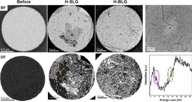
Dark-field TEM (DF-TEM) specializes in structural transformation because it allows the region of the specimen outside the Bragg state to be illuminated only such as dislocations and bending regions in single-crystal specimens. EELS spectra representing stacking enhancement in 100 layer - graphene systems annealed at (a) 400 ºC and (b) 2800 ºC. Broadening and bending of moiré fringes of G/hBN only in low θG-BN in (a) DF-TEM and (b) AR-TEM images.
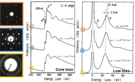
Comparison of the moiré edges between small and large θG-BN by masking on AR-TEM images. Simulated AR-TEM images for (a) defocus conditions and (b) interlayer distances depending on the stacking configurations. Electron diffraction patterns of NCM 622 (a) in the interior and (b) in the surface region of the primary particle.
Graph of the depth of disorder on the surface of NCM 622 as a function of cycles. Different morphologies and cross section of secondary particles of NCM 721 according to the types of electrolyte additives after the 100th cycle.
TWO-DIMENSIONAL MATERIALS
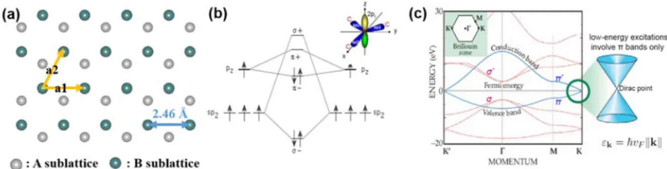
Interatomic Interaction on Two-Dimensional Superstructures
Intensity variation depending on the stacking structure and the number of layers in the DF-TEM image of the multilayer graphene. The moiré fringes in the DF-TEM images and those in the masked AR-TEM image. A schematic of contrast in the moiré fringes caused by interference between the lattice fringes of graphene and hBN in DF-TEM depending on the stacking configuration.
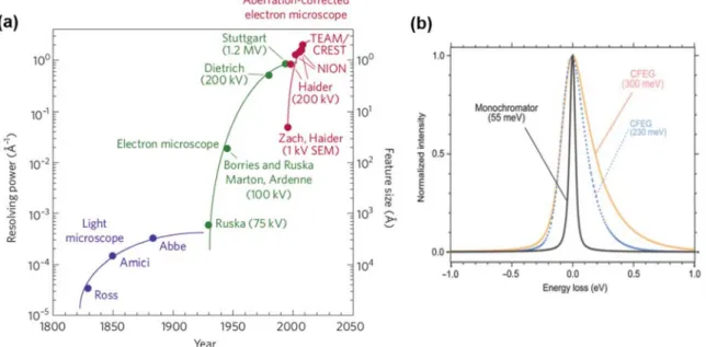
As shown in Figure 2(a), the electron wavelength must be reduced to improve resolution by increasing the microscopes' acceleration voltage up to 1 MeV or higher.3 The increased voltage also increases the penetration depth of the electrons, making it possible to analyze much thicker samples. The distribution of the moiré fringes during DF-TEM immediately gives the interlayer relation through twist angle between stacked layers. As the number of graphene layers increases, the intensity of the DF-TEM image increases in the 2nd order diffracted reflection (I2) regardless of the stacking configuration (Figure 28).
Therefore, the general moiré fringes can analyze the real distribution of the superlattice domains and grain boundaries in the single 2D system. In Method 1, the diffraction vector of the generalized moiré fringe (ggm) is perpendicular to the moiré fringes in real space. The orientation of the moiré fringes and distribution of dgm are highlighted by the yellow line and magenta box, respectively.
Broadening and bending of the moiré edges of G/hBN only at low θG-BN in (a) DF-TEM and (b) AR-TEM images.73. For large θG-BN (θG-BN = 3.2°), the moiré edges are evenly distributed in all orientations, in other words, all dgm in three orientations are consistent and equal to 3.66 nm. The period of the oscillation depends on the excitation error and the thickness of the specimen.
Therefore, the masking technique on the AR-TEM image is suitable to investigate the interaction between the layers by corelating with the moiré edges in the DF-TEM image. Comparison of the moiré edges between small and large θG-BN by masking on AR-TEM images.73. Figure 42 shows the different morphology of the moiré edges between small and large θG-BN.
A scheme of the contrast in the moiré edges caused by interference between the lattice edges of graphene and hBN in DF-TEM depending on the stacking configuration.73. The raster edge images of monolayer graphene and monolayer hBN were intentionally stacked to demonstrate the relationship between the stacking configuration and the morphology of the moiré edges (Figure 47). Simulated AR-TEM images of G/hBN for (a) defocus conditions and (b) interlayer distances depending on the stacking configurations.73.
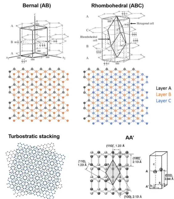
The local morphology variation of the moiré edges shows that the transition to the proportional state occurs by reducing lattice mismatch and twist between the graphene and hBN in the AB-stacked regions.
DEGRADATION MECHANISM OF LAYERED CATHODE MATERIALS IN
Reaction Between Electrode Materials and Electrolytes
Low-loss EELS is suitable for the study of low degree of functionalization and weak C-H bonds. The acquisition time of DF-TEM and atomic resolution TEM images was 5 and 0.3 s, respectively. However, small changes in μ become large morphological differences in moiré fringes, which are reciprocally related to μ; thus the dgm and the width of the moiré fringes also become noticeable.
It indicates a significant decrease in the (003) peak intensity, which means a random distribution of cations at the 3a (Li) and 3b (Ni) sites of the R-3m. In other words, this indicates non-uniform cation ordering and collapse of the layered structure in the surface region. The increase in L3/L2 intensity ratio can be interpreted as lower surface oxidation states.
For example, solid electrolyte interphase (SEI) and solid permeable interface (SPI) are formed on the surface of the anode and cathode by the side reaction with electrolytes, respectively. On the other hand, it has not been intensively established to investigate how to weaken the microstructure of cathode materials depending on the types of electrolyte additives. Even though the secondary particles retain their spherical morphology, there are micro-cracks on the surface and also on the diameter of the secondary particles.
The high density of cracks in the secondary particles indicates that the cracks have synergistic effects on the fragmentation of the primary particles.138. PS retains rhombohedral structures like R3m even for primary particles located on the outermost secondary particles. I am interested in the scientific investigation of the local structural transition of layered materials using aberration-corrected transmission electron microscopy (TEM).
Lee, “Impact of the types of electrolyte additives on the microstructural degradation of Ni-rich cathode materials in lithium-ion batteries” will be submitted. Lee, “Local Lattice Match for Commensurate State Transition of Graphene/hBN van der Waals Heterostructure”, The 5th International Conference on Electronic Materials and nanotechnology for Green Environment (ENGE Jeju, Korea. Lee, “Evidence of Local Lattice Match of Graphene on Hexagonal Boron Nitride ”, The 10th International Conference on Advanced Materials and Devices Jeju, Korea.
Lee, "Atomic Scale Study on Growth and Heteroepitaxy of ZnO Monolayer on Graphene", The 3rd East-Asia Microscopy Conference Busan, Korea. Lee, "Surface Oxidation of Atomically Thin MoS2 by UVO treatment", The 3rd East-Asia Microscopy Conference Busan, Korea. Elektrokemisk cykling ved analytisk TEM og STEM”, Den 3. østasiatiske mikroskopikonference Busan, Korea.
Spinel phase formation in a multilayer composite cathode used in Li-Ion batteries.