Introduction
Background
Motivation and Problem Statement
Project Scope
Project Objectives
Significance and Impact
Literature Review
MIPS
MIPS is widely used in digital consumer, networking, personal entertainment, communications, and business applications [2] such as the Sony Playstation 2, Sony Playstation Portable (PSP), and the Linksys wireless router, which is primarily used in MIPS implementations.
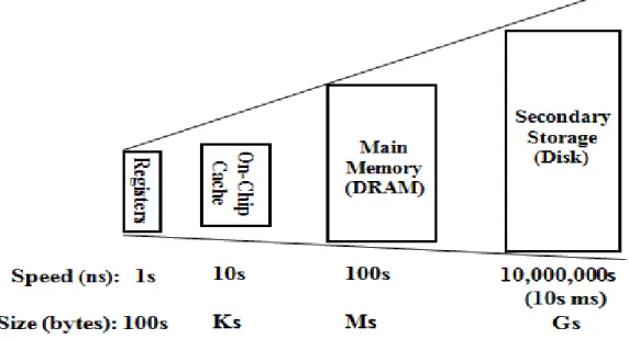
Memory Hierarchy
Faculty of Information and Communication Technology, UTAR Page 7 separates individual levels according to access time, price per unit and capacity. In addition, the control technology plays an important role in creating memory with faster access time, so each level of the memory hierarchy can also be used to differentiate the control technology [2,3,6,8].
Cache and Main Memory Interfacing
With all the above information, we can evaluate the performance of the memory organization shown in Figure 2.3.1. For a single word memory organization, since it can only fetch one word at a time, in other words it means that the main memory has to be accessed 4 times to fetch all the data needed for the cache. For wide storage organization, it is able to retrieve all the required data in one shot, as it has a very high bandwidth of the leading system.
Finally, an interleaved memory organization that can read multiple words in main memory in a single bus cycle and transfer the data back word by word. Faculty of Information and Communication Technology, UTAR Page 9 penalty, but remember that a huge bus system is not easy to manage and requires high costs to implement. Interleaved memory organization, although slower than wide memory organization, uses a shared bus system between memory banks.
This reduces the implementation cost, but it will result in similar performance to wide memory organization.
DRAM
SDRAM
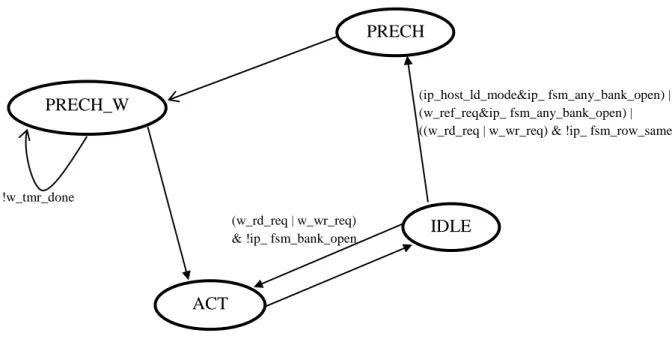
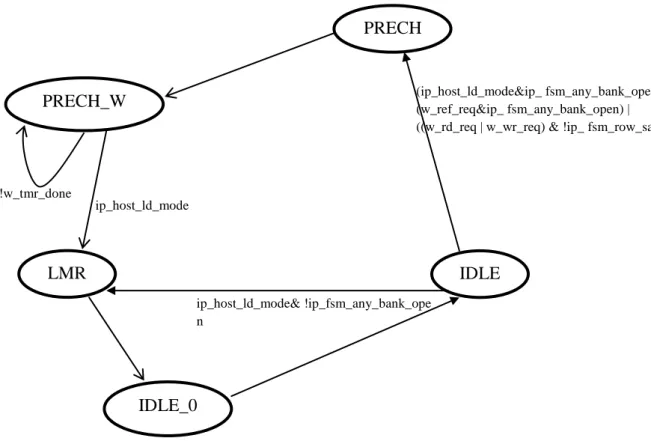
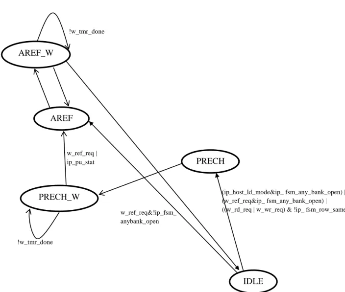
SDRAM Controller
Problem in Existing Memory System
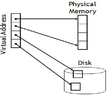
For the existing memory system, they actually use physical address to access the information residing in either SDRAM or caches. Noticed that all the currently running process must be in main memory. To solve the problems we can enlarge our main memory or the programmer must bear the responsibility of dividing the program they had written into few sections and transfer them to the main memory.
As the program progresses, new sections will be added to main memory, replacing the sections that are currently unused. As the program becomes more and more complex, it is impossible for programmers to handle the division of the program.
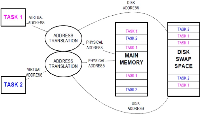
Introduction of Virtual Memory
Overview of Virtual Address Space
In this design, the address used will be virtual address and must undergo address translation before it can access memory. Faculty of Information and Communication Technology, UTAR Page 32 For virtual memory, the memory space is divided into a few segments as shown in the figure below.
Concept of Address Translation
Introduction of Page Table
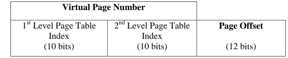
Faculty of Information and Communication Technology, UTAR Page 36 In the figure, since we use only one page table which is all called a 1-level page table, the size of the page table will therefore be . That is memory waste where too much space is wasted building a page table. Therefore, another technique is used to reduce the waste of memory, which is called a 2-level page table.
The concept of using a 2 level page table is that the first level of the page table contains the page table entries listed below. Physical page number is part of the physical address that must be output to merge with the page offset. Faculty of Information and Communication Technology, UTAR Page 37 By using the 2-level page table technique, we need to segment the virtual address into, .
1st Level Page Table Index is used to locate the address of the 2nd level Page Table. By segmenting the virtual page number into 1st level page table index and 2nd level page table index, we can find the desired items in the page table as below. Faculty of Information and Communication Technology, UTAR Page 38 As can be seen in the figure, the size of the page table has been significantly increased compared to the 1 level page table.
Previously, if we used a 1-level page table, we had to allocate 4 MB of page table space for each process. On the other hand, when we use a two-level page table, we only need to allocate 8 KB of space for the page table, and the page table can be created on demand. In addition, using this mechanism, the size of the page table will be equal to the size of the pages in virtual or physical memory.
Introduction of Translation Lookaside Buffer
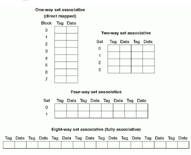
Faculty of Information and Communication Technology, UTAR Page 39 The key to improving performance is to rely on the location of the reference in the page table. With this concept, the TLB is introduced, which is a special memory for translation that the entire entry part of the page table enters in order to speed up the translation of addresses. To enable a faster access table, the TLB usually contains only much fewer entries which are around 48-128 entries and because of this, the TLB is usually implemented as a fully associative cache, which all entries within the TLB will be compared in one snapshot.
This will result in a faster search speed, but it may require a lot of hardware support to build it. Faculty of Information and Communication Technology, UTAR Page 40 Figure 2.12.2: Example of how a search works on an eight-block cache based on direct. Now, in order for us to start implementing the TLB, the first thing we need to do is identify the contents of each entry in the TLB.
For a basic TLB we need to have VPN, PPN and also some control bits which are used to indicate the status of each record such as valid bit, dirty bit and so on based on the design needs. Faculty of Information and Communication Technology, UTAR Page 41 Figure 2.12.4: Use of TLB in address translation using 48 entries and in full. The VPN is included inside as part of the TLB entry's content, which is different from the page table entry.
This is because when we use TLB it only contains the information in 2nd level page table. Control bits can be any bits that used to represent the status of each input based on the design needs. Valid Bit, which used to represent the location of the page, whether it was in physical memory or disk.
The ref bit, which is an LRU status where the entry with the lowest ref will be replaced when the CPU fetches a new page from disk or physical memory.
Virtually Addressed and Physically Addressed Cache
Methodology& Development tools
Methodology
Faculty of Information and Communication Technology, UTAR Page 44 Figure 3.1.1: The top down approach used in this project. Subblocks that do not work as specified must be debugged and their RTL codes must be corrected, the requirements are met. After the main task of defining the functionality is completed, the design is synthesized to gate-level representation.
Development Tools
Handling Virtual Memory
Address Translation to Instruction Cache without TLB
Address Translation to Data Cache without TLB
Address Translation to Instruction Cache with TLB
Address Translation to Instruction Cache with TLB
Memory System Specification
- Features of Memory System
- Memory Map
- Memory Unit Interface
- Memory System Operating Procedure
Faculty of Information and Communication Technology, UTAR Page 55 Control signal to allow manual entry of data into SDRAM.
Architecture Specification
- Unit Partition of Memory System
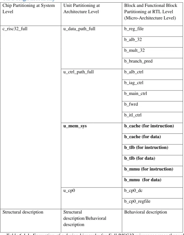
- Design hierarchy
- Memory Unit
- CP0 unit
- SDRAM Controller
Faculty of Information and Communication Technology, UTAR Page 62 Figure 6.2.1: Complete RISC32 architecture and micro-architecture partitioning. Faculty of Information and Communication Technology, UTAR Page 64 Overview of CP0's register used in Memory System. Note that the previous SDRAM controller design is based on 16 MB SDRAM provided by Micron.
Micro-Architecture Specification
Translation Lookaside Buffer (TLB)
The Translation Lookaside Buffer is like a cache that holds some of the page table entries which can reside either in physical memory or on disk. Its responsibility includes translating the virtual address provided by the CPU to a physical address and ensuring that any user process does not have access to the kernel segment. Based on what we discussed in the previous chapter, we know that address translation is important for us to get the physical address used to write or read data.
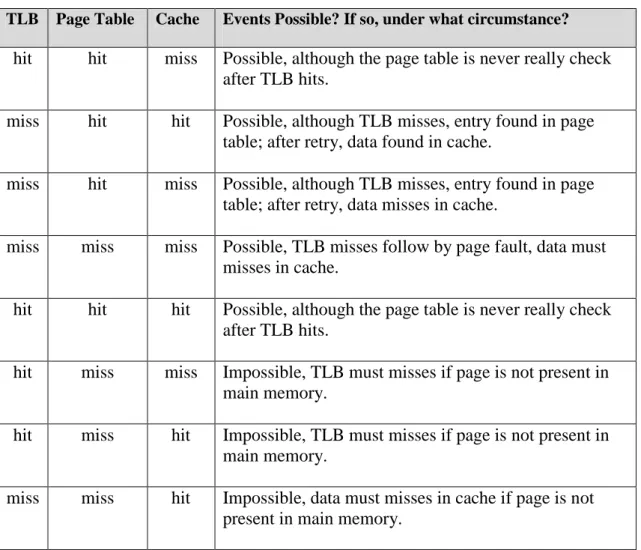
On the other hand, it means that the data must be present in the main memory only to be able to access the cache. To discuss this further, the table below gives us the simplest way to examine the relationship between cache and TLB.
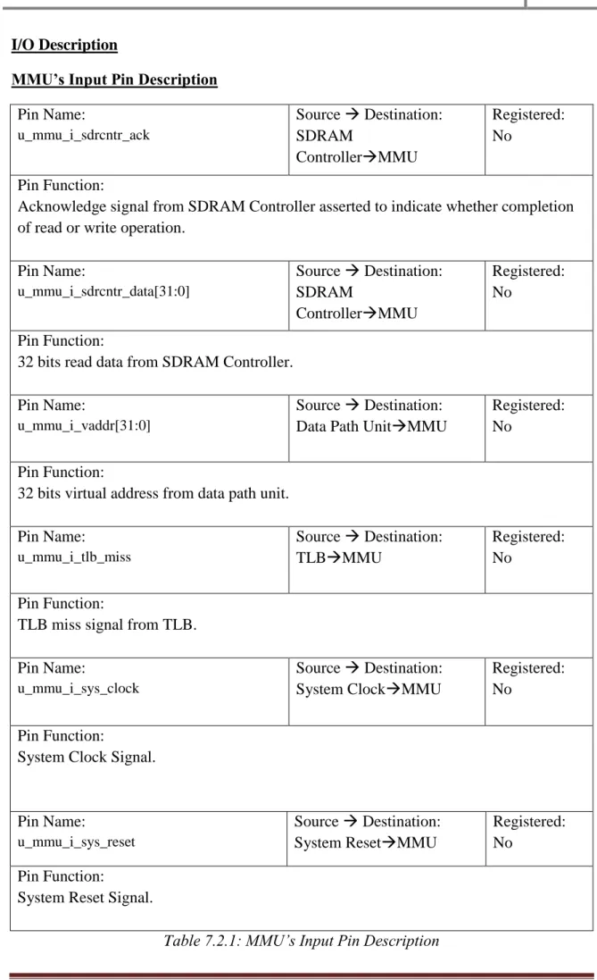
Memory Management Unit (MMU)
Assert the signal from the SDRAM controller to indicate whether the read or write operation is complete. 1 bit signal to indicate the end of TLB loss by sending the signal to CP0 and CP0 will restart the instruction by loading the address store into the EPC register. It is used to indicate where valid data is placed on the input data line (ip_wb_dat) during the WRITE cycle and where it should appear on the output data line (op_wb_dat) during the READ cycle.
Faculty of Information and Communication Technology, UTAR Page 89 Output for each state in the MMU protocol.
Verification Specification
Test Plan of Memory Unit
- Test Procedure
Insert data into SDRAM using the test signal, u_mem_sys_test_insert_data_en, u_mem_sys_i_test_data and u_mem_sys_i_test_addr.
Simulation Result for Memory System
- Load Page Table and Page to SDRAM
- ITLB MISS
- DTLB MISS
- Instruction Cache Miss
- Data Cache Miss
Discussion and Conclusion
Discussion & Conclusion
Future Works
9] Zhi Kang Oon, “SDRAM Enhancement: Design of a SDRAM Controller WISHBONE Industrial Standard” University of Tunku Abdul Rahman, Faculty of Information and Communication Technology, 2008.
![Figure 2.2.1: The Memory Hierarchy(Adapted from [6])](https://thumb-ap.123doks.com/thumbv2/azpdforg/10216049.0/17.918.146.789.612.977/figure-the-memory-hierarchy-adapted-from.webp)
![Figure 2.5.1: Block diagram of 128Mb banks SDRAM(Adapted from [9]) Pin Name Size Description](https://thumb-ap.123doks.com/thumbv2/azpdforg/10216049.0/21.918.333.581.330.577/figure-block-diagram-banks-sdram-adapted-name-description.webp)
![Table 2.6.2: State Definitionsof Protocol Controller Block(Adapted from [9]) Output or Behaviors of Protocol Controller Block Corresponding to the States](https://thumb-ap.123doks.com/thumbv2/azpdforg/10216049.0/31.892.94.765.144.570/definitionsof-protocol-controller-adapted-behaviors-protocol-controller-corresponding.webp)