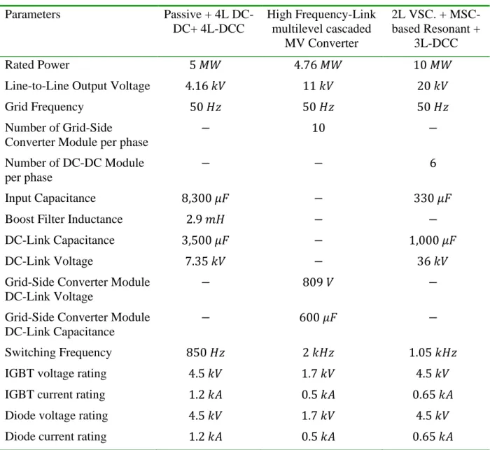
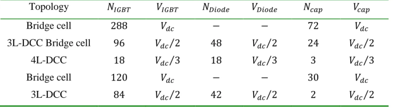
The efficiency of the proposed converter topology has been evaluated by varying the switching frequency and the loads. 247 6.9 Comparison of the proposed converter topology with a conventional converter topology in terms of component count……….
Glossary of Abbreviations and Symbols
Symbols
𝑁 Life expectancy of WPP/transformer 𝑁𝐴 Number of turns of the active bridge 𝑁𝑐𝑎𝑝 Number of capacitors. 𝑅𝑀𝑉𝑐 Resistance of the medium voltage connection cable 𝑅𝐻𝑉𝑐 Resistance of the high voltage connection cable 𝑅𝑇𝐻ℎ Thermal resistance of the heatsink.
Introduction
Overview of Reliability Studies on WECS
The electrical subsystem showed the highest failure rate in both onshore and offshore WPPs, as illustrated in Figure 1.2 [24]. Another reliability study was conducted based on the electric generator technology deployed in the WECS [25].
Operational Year
- Electric Generators
- Power Converter Topologies
- Electrical Subsystem
- Motivation for Research
- Problem Statement
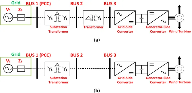
- BUS 2
- PCC)Grid
- PCC)
- Voltage conversion ratio between the generator-side and the collection point
- Voltage rating of the power semiconductor devices and number of clamping devices
- Minimization of DC Component
- Cost-Effectiveness
The design challenges to implement a multi-level converter topology on the grid side of the power converter configuration of the transformerless WECS. A comprehensive survey of the existing current converter configurations for transformerless WECS was carried out.
![Figure 1.4: A direct drive WECS [27].](https://thumb-ap.123doks.com/thumbv2/pubpdfnet/10366833.0/35.892.172.711.748.1054/figure-a-direct-drive-wecs.webp)
Power Converter Configuration Overview and Cost- Benefit Analysis
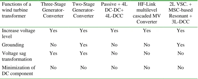
- Functions of Transformers in a WPP
- Voltage level transformation
- Grounding
- Voltage sag transformation
Other types of voltage dips (ie, Type D, Type F, and Type G) are derived from the original dip based on the transformer winding connections that exist between the fault location and the WECS terminal. While the substation transformer consists of grounded-wye/grounded-wye/delta connection (𝑌𝑔∆𝑌𝑔) [48].
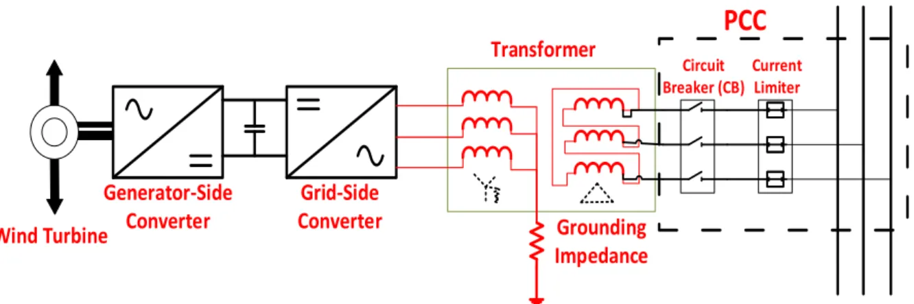
PCC (BUS 1) Substation Transformer (BUS 2) Transformer (BUS 3)
Minimization of DC component
- Classification of Power Converter Configurations
- Generator-Converter Configuration
The three-phase power converter configuration consists of a conventional electric generator and a three-phase power converter that steps up the voltage level of the generator-side converter to the MV level of the grid-side converter [88]-[90] . An MMC topology module consists of generator-side converter and grid-side converter topologies, as shown in Figure 2.5.
Three-Stage Generator-Converter Configuration
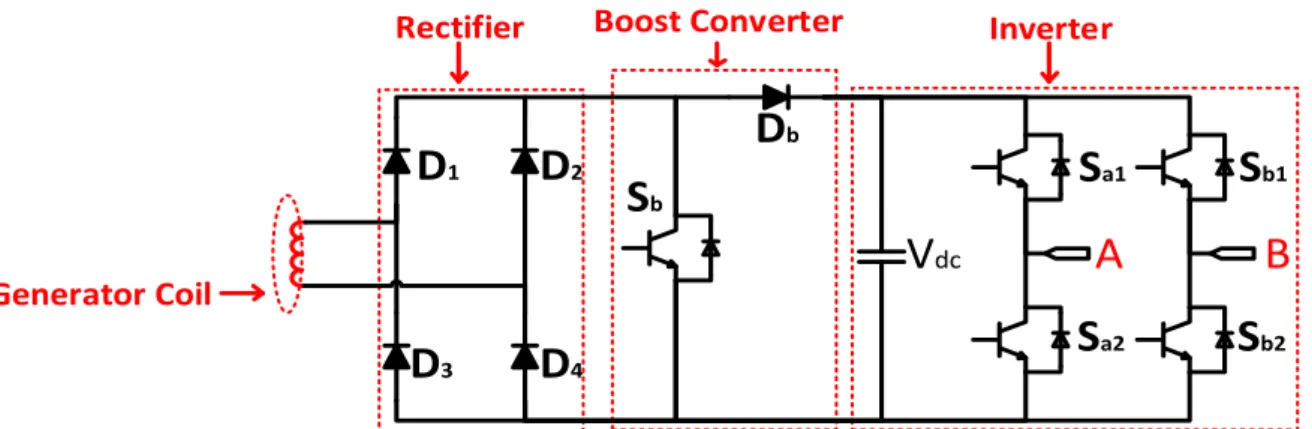
In Figure 2.8(a), the two stator coils and their respective single-switch boost converters are connected in parallel at the generator side providing constant power to the DC switching capacitors [86]. The biggest advantage of deploying the structure in Figure 2.8(b) is that the DC link voltage of each module.
Two-Stage Generator-Converter Configuration
S b2Vdc
Three-Stage Power Converter Configuration
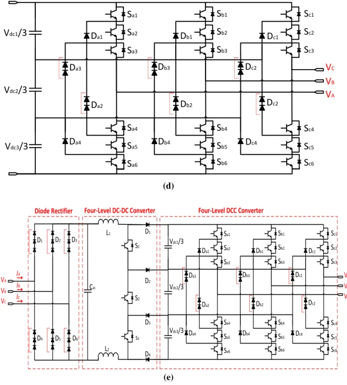
Passive Generator-Side with 4L DC-DC Converter and 4L-DCC
BVOUT
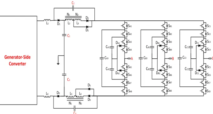
However, the variable switching frequency of the model's predictive control strategy results in increased harmonics in the output current [97]. A diode rectifier, 4L DC-DC boost converter and 4L-DCC configuration. a) block diagram of the configuration, (b) three-phase diode rectifier, (c) four-level DC-DC boost converter, (d) four-level DCC topology, and (e) circuit of the configuration.
R 3VIN
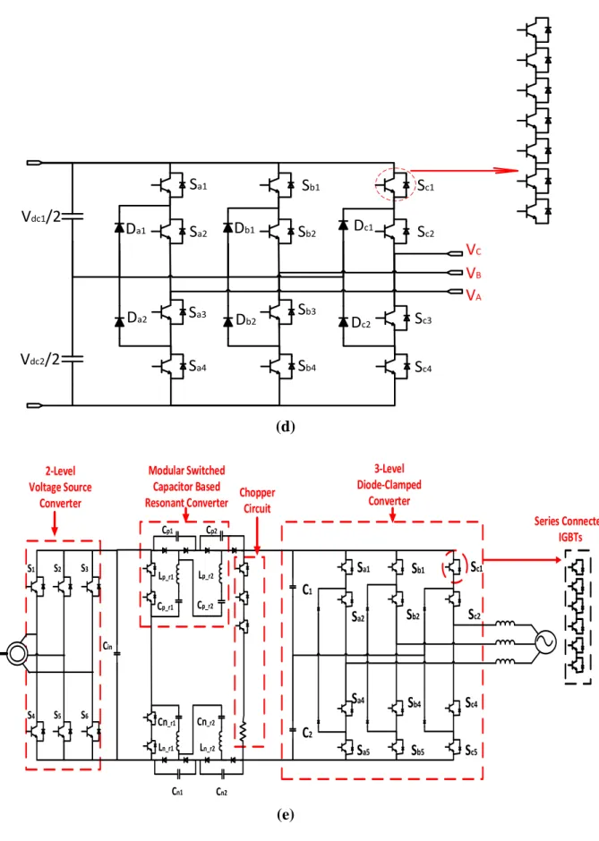
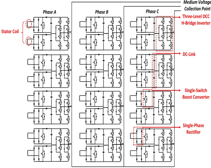
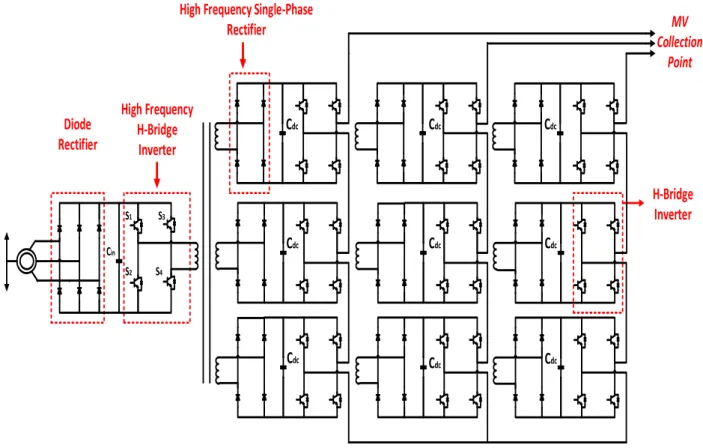
High Frequency-Link Multilevel Cascaded Medium-Voltage Converter
In the second mode of operation, the diode modules (𝐷2 and 𝐷4) conduct on the 𝐻𝑉 side of the topology, as shown in Figure 2.15(b). In addition, in the fourth mode of operation, the diode modules (𝐷2 and 𝐷4) on the 𝐻𝑉 side of the converter conduct, as shown in Figure 2.15(d).
V OUT V IN
Comparative Evaluation
- Device Count
- Voltage Boosting Topology
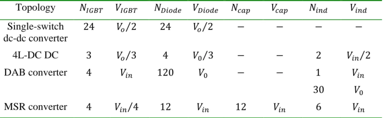
Power converter configurations are evaluated in terms of device count, voltage gain topology, and grid compliance. The number of units directly affects the reliability and cost of the current converter configuration, as illustrated in Figure 1.6.
Non-isolated DC-DC Converter
Isolated DC-DC Converter
Furthermore, dead time during the switching intervals of the IGBTs on the LV side of the DAB converter (as shown in Figure 2.15(a) to 2.15(d)) introduces an additional unwanted phase shift [112]. This negative effect inherently limits the power flow between the LV side and HV side of the DAB converter.
Soft-switching DC-DC Converter
- Grid Compliance
- Comparative Benchmark Factor (CBF)
The elimination of the step-up transformer in the transformerless WECS configuration reduces the overall reactive power of the WPP. However, the reactive power of the converter configuration can be improved through advanced modulation and control techniques [16].
Component for each Level Factor (𝐶𝐸𝐿 𝑓 )
Therefore, the component for each level factor (𝐶𝐸𝐿𝑓), presented in [114], is extended to the converter on the generator side, the intermediate boost converter and the converter on the grid side of the configuration. In Tables 2.7 through 2.9, the value of 𝑉𝑏 depends on what part of the configuration the component is in (that is, the netside converter topology will have 𝑉𝑏 𝑉𝑑𝑐, while the intermediate boost converter topology will have both 𝑉𝑖𝑛 and 𝑉𝑜 will have that 𝑉𝑏 based on topology and the component).
Grid Compliance Factor (𝐺𝐶 𝑓 )
57 the injection of the dc components is directly related to the asymmetric characteristics of the switching power semiconductor devices (i.e., IGBTs), and the THD is related to the number of voltage levels in the converter topology on the network side of the power converter configuration. In Table 2.11, a comparison of 𝐺𝐶𝑓 in the presented power converter configurations for all voltage levels of the grid-side converter topology is shown.
Summary of the Comparative Benchmark Factor
- Cost-Benefit Analysis
- LCC Analysis of the Power Converter Configurations
The life cycle cost (LCC) analysis of the power converter configuration in a transformerless WECS is compared with the power converter configuration in a conventional WECS. The total cost of the power converter configuration is classified into three main components, namely initial cost (𝐶𝑖), operation and maintenance cost (𝐶𝑂&𝑀) and energy cost (𝐶𝑒).
Initial Cost (𝐶 𝑖 )
The impact of six series-connected switching power semiconductor devices, which further increased the number of components, will further increase the complexity of the configuration. In addition, the LCC analysis of WPP collection system with transformerless WECS and conventional WECS is presented to determine the cost benefits of WPP with transformerless WECS.
Operation and Maintenance Cost (𝐶 𝑂&𝑀 )
Energy Cost (𝐶 𝑒 )
Cost Comparison and Discussion
Based on Figure 2.22, the three-phase three-step generator-converter configuration is the most expensive due to its MMC topology and high power ratings of its power semiconductor devices. On the other hand, the passive generator side with 4L DC-DC converter and 4L-DCC configuration is the cheapest among configurations installed in a transformerless WECS.
Summary of the Cost Benefit Analysis
- LCC Analysis of the Collection system of a WPP
However, the total cost associated with the 3-step two-step generator-converter configuration is about 42% less than the total cost of the 3-step three-step generator-converter configuration, as shown in Figure 2.23. The same trend occurs with the total cost associated with the 3-level two-level generator-converter configuration being about 10% less than the total cost of the high-frequency link multilevel cascaded MV converter configuration, as shown in Figure 2.23.
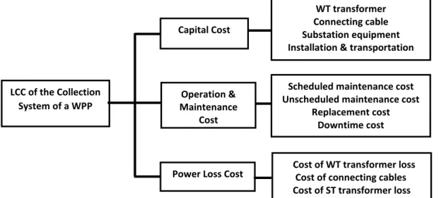
Capital Cost (𝐶 𝑖𝑛𝑣 )
Operation and Maintenance Cost (𝐶 𝑜𝑝 )
Power Loss Cost (𝐶 𝑙𝑜𝑠𝑠 )
- Case Study
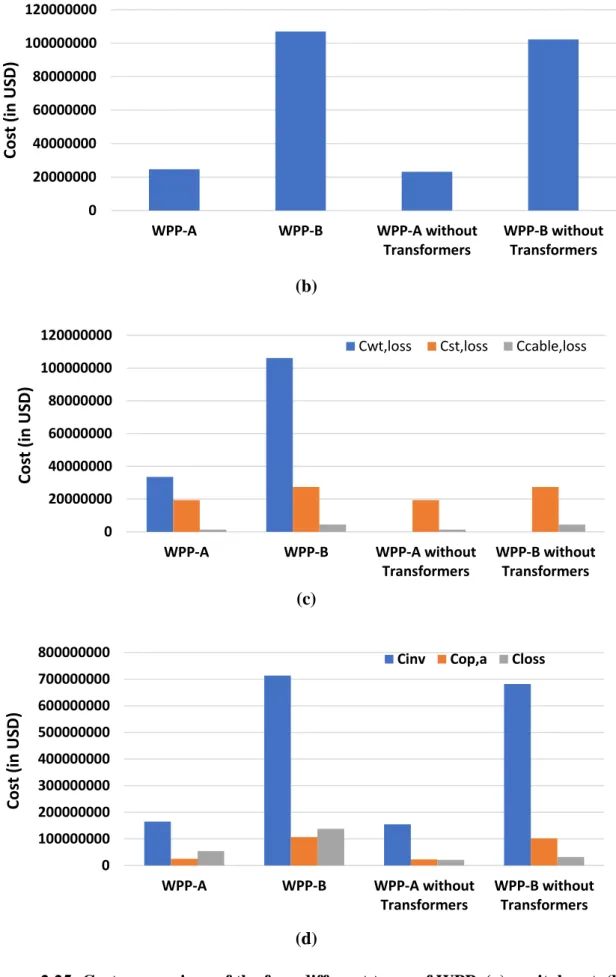
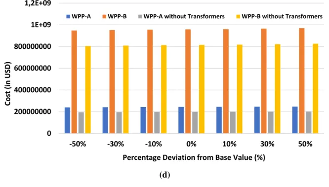
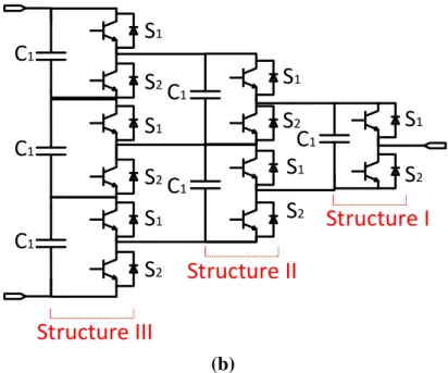
69 connecting cable, 𝐸𝑒 energy cost per unit, 𝑂𝑝𝑎 is the transformer's operating hours per year, 𝑖 is the interest rate, 𝑁 is the expected lifetime of the transformer, and 𝐿 is the transformer load. In this section, the LCC model presented in section 2.4.2 is used to analyze the associated costs of the collection system of two existing WPPs (i.e. WPP-A and WPP-B).
Comparative Evaluation
Furthermore, the power loss cost of the transformerless WPP-B collection system is about four times the power loss cost of the WPP-B collection system. Moreover, the total cost of WPP-B collector system without transformer is about 18% less than the total cost of WPP-B collector system.
Sensitivity Analysis
- Conclusion
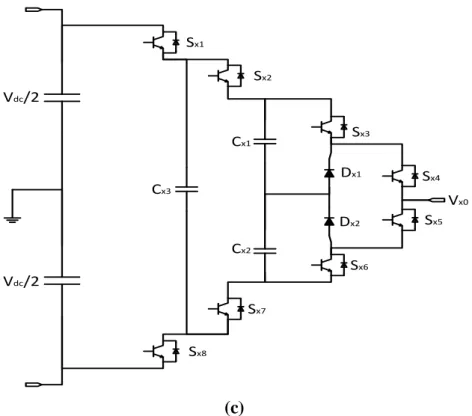
An increase of 50% in WPP-A and WPP-A without transformers, respectively, results in the total costs of the WPP-A collection system without transformers being approximately 22.2% lower than the total costs of the WPP-A collection system. 76 A sensitivity analysis of four main parameters (namely: number of wind turbines, power of the wind turbine, length of the collector cable and the costs of substation equipment) was also studied that influence the total costs of a WPP's collection system. .
Nested Neutral-Point-Clamped (NNPC) and Modified NNPC Converter (MNNPC)
Background and Derivations
- Derivation of a Four-Level NNPC Converter Topology
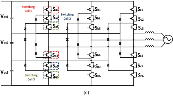
The generalized multilevel topology consists of two-level converter cells with complementary IGBT modules, as shown in Figure 3.1(a). Based on the generalized 1ph four-level (4L) multilevel topology shown in Figure 3.1(b) and the stated derivation principles, a 1ph 4L-NNPC converter topology is derived with minimized clamping devices.
Operating Principle
Mathematical Model
CVdc/2
Derivation of a Five-Level NNPC Converter Topology
Each topology IGBT is rated at a quarter of the dc link voltage, while the internal clamping capacitors (𝐶𝑥1and. 𝑉𝑑𝑐 is the dc link voltage; 𝑉𝝑𝑥1, the voltages across the clamping capacitors and 𝑖𝑥 represents the output phase current.
Derivation of a Seven-Level MNNPC Converter Topology
Stage A
Outer Structure
Inner Structure
Stage B
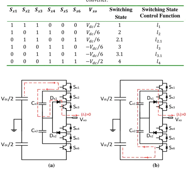
The topology of the 7L-MNNPC converter consists of twelve power semiconductor devices and two clamping capacitors per phase. The combinations of switching states to achieve the output voltage waveform of the 7L-6 MNNPC inverter topology are presented in Table 3.3.
Stage C
Converter Design
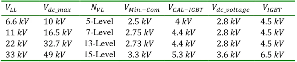
- Specification and Constraints
This section presents the design specification and associated limitations of the converter topologies used as a grid-side converter in a transformerless WECS. The first step of the NNPC converter design for transformerless WECS is to define its specifications in two main categories: primary and secondary specifications [135].
Primary Specifications
Secondary Specifications
- Modelling and Control Strategy
This subsection presents the average mathematical model of the 4L-NNPC, 5L-NNPC, and 7L-MNNPC converter topologies, respectively. Also presented is the voltage balancing control strategy of the clamp capacitors in a 5L-NNPC converter topology.
Averaged Mathematical Model
The switching state control function 𝑙𝑚 (where 𝑚 represents the actual switching state of a specific voltage level of the converter topology. Therefore, the switching control functions in equations (3.1) to (3.3) are replaced by the product of the switching state control functions and associated duty cycle variables of the voltage level when.
Voltage Balancing Control Strategy for Clamping Capacitor
Therefore, the clamp capacitor voltages of the converter topology will naturally be balanced under ideal conditions. For example, the current flowing through the clamping capacitor 𝐶𝑥3 of the five-level NNPC converter topology (𝑖𝑐𝑥3) expressed in (3.5) is dependent on the switching power semiconductor devices 𝑆𝑥1 and 𝑆𝑥2.
Grid-side Control Strategy
The voltage changes at the PCC due to the active and reactive power transferred between the converter and the network and the load power is expressed in . the powers transferred to the grid can be obtained as follows:.
Reactive Power Capability
- Component Rating Analysis
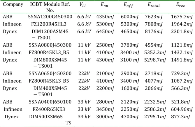
Power Semiconductor Device Ratings
The values of 𝐼𝑝 and the calculated current (𝐼𝐶𝐴𝐿−𝐼𝐺𝐵𝑇) of the IGBT modules are obtained using (3.55) and (3.56), respectively. Therefore, 𝑉𝐷𝑖𝑜𝑑𝑒 and 𝐼𝐷𝑖𝑜𝑑𝑒 for each medium voltage level of the assembly point are marked in Table 3.11.
Selection of Power Semiconductor Devices
- 𝑘𝑉 6450𝑚𝐽 4650𝑚𝐽 8176𝑚𝐽 2301.8𝑚𝐽 ABB 5SNA0800J450300 11 𝑘𝑉 2580𝑚𝐽 3780𝑚𝐽 4554𝑚𝐽 1121.8𝑚𝐽
- 𝑘𝑉 713 𝑊 1301 𝑊 366.3 𝑊 2380.3 𝑊 ABB 5SNA0800J450300 11 𝑘𝑉 545.4 𝑊 725 𝑊 178.5 𝑊 1448.9 𝑊
The value of the thermal resistance of a heat sink (𝑅𝑇𝐻ℎ) depends on 𝑇𝑗, the ambient temperature (𝑇𝑎), and the corresponding thermal resistance of the IGBT module, as shown in Figure 3.15. From the analyzes presented in this section, Table 3.18 lists the most appropriate IGBT modules for an NNPC and MNNPC converter topology connected directly to the collection points of a WPP.
Clamping Capacitors
The capacitance of the clamping capacitors in the 7L-MNNPC converter topology (as shown in Figure 3.6(c)) is obtained from (3.60).
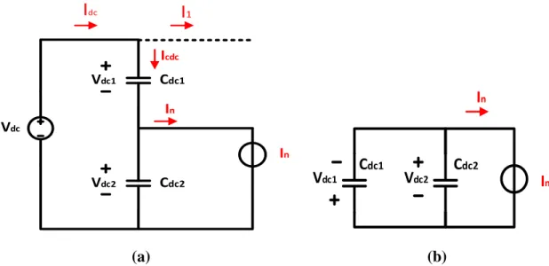
DC-Link Capacitors
- Simulation Results
- Design Verification
- Grid connection scenarios
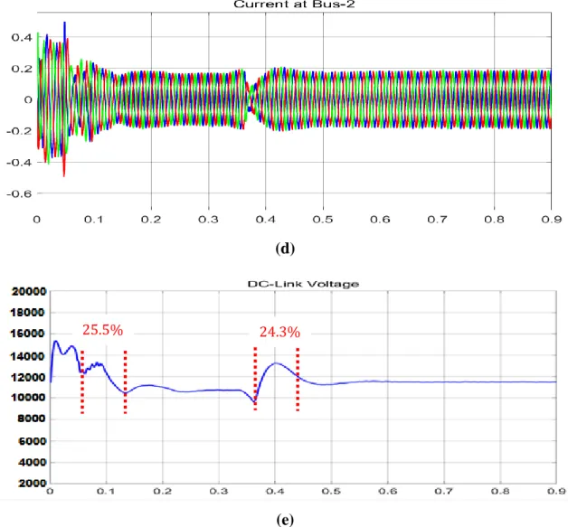
In the simulation results presented, the maximum DC link voltage of the NNPC and MNNPC converter topologies is assumed to be constant. The results are performed and observed under three different scenarios, namely: (a) voltage drop propagation in a conventional WPP, (b) voltage drop propagation in a WPP with transformerless WECS, and (c) impact of voltage drops on the DC link voltage of the inverter on the grid side.
Voltage Sag Propagation in a Conventional WPP
Detailed analysis of the voltage sag transformation within a conventional WPP and a WPP with transformerless WECS is presented based on simulations performed in the MATLAB/Simulink environment.
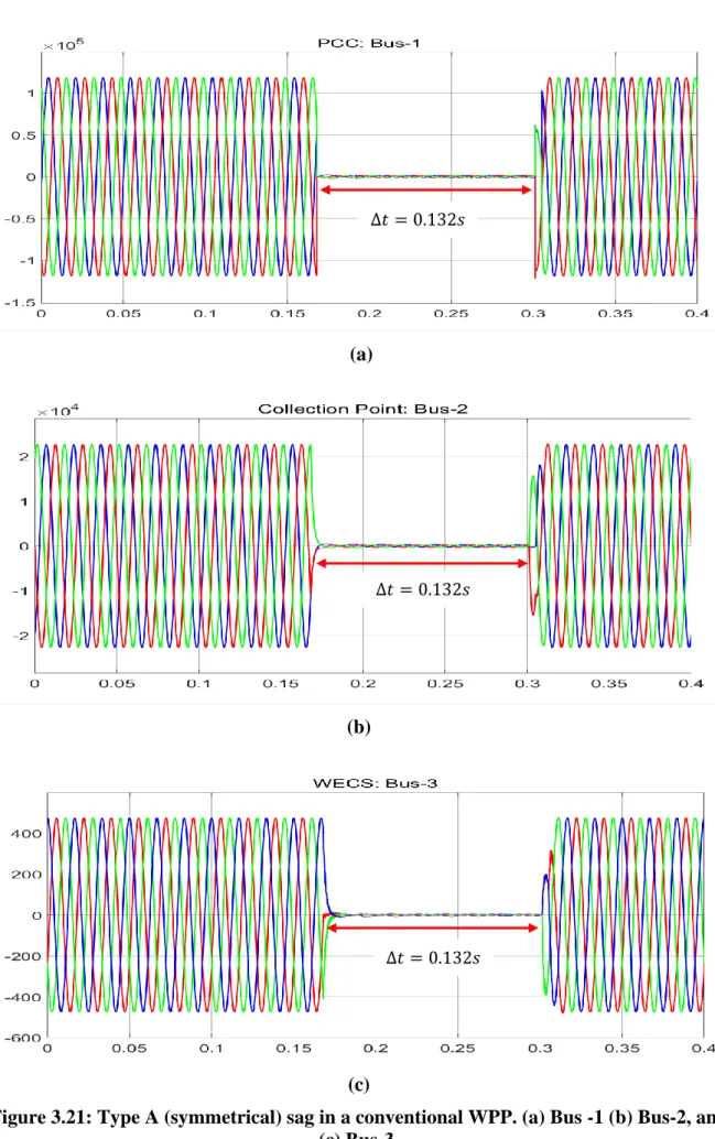
Voltage Sag Propagation in a WPP with Transformer-less WECS
Impact of Voltage Sags on the DC-Link Voltage of the Grid-side Converter
- Conclusion
In this chapter, the NNPC and MNNPC converter topology is proposed for the converter on the grid side of the WECS configuration without a transformer. A theoretical analysis and simulation of the NNPC and MNNPC converter topology installed on the grid side of a transformerless WECS configuration is presented.
Tapped Inductor Quasi-Z-Source NNPC Converter Topology
Introduction
The quasi-Z-source converter includes a quasi-resistance source network and semiconductor power devices, as illustrated in [171]. A dual-inductor quasi-source Z converter topology (as shown in Figure 4.1(a)) was chosen for a low-voltage solar photovoltaic (PV) application because it provides a high boost factor while maintaining a relatively low modulation index. important [ 176].
Operating Principle
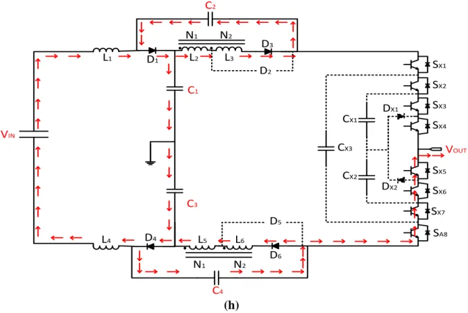
The two tapped inductor quasi-z source (qZS) network consists of two inductors, two tapped inductor (TI) cells (a TI cell consists of a coupled inductor and two diodes as shown in Figure 4.3(a )), two gate diodes (𝐷1 and 𝐷4) and four capacitors (𝐶1, 𝐶2, 𝐶3 and 𝐶4), as shown in Figure 4.2. These tapped inductor quasi-impedance source networks are arranged in a "T-shape" network in the positive and negative rail of the converter topology.
Shoot-Through (ST) Mode
Non-Shoot-Through (NST) Mode
- Steady-state Analysis
- Design of the tapped inductor quasi-Z-source network
- Deriving the Values of the Capacitance and Inductance
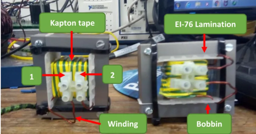
- Inductor and Tapped Inductor Design
The switching period of the proposed 5L tapped inductor qZS-NNPC converter topology is categorized into two switching states (as expressed in 4.24) and thirteen possible switching states as illustrated in Table 4.1. Furthermore, the proposed converter topology will have a significant increase in its voltage conversion ratio when the turns ratio of the tapped inductors is greater than unity (𝑁 ≥ 1).
Specification
This section presents the step-by-step process for input inductor and tapped inductor design based on area-product (𝐴𝑝) method as illustrated in Figure 4.9.
Core Selection
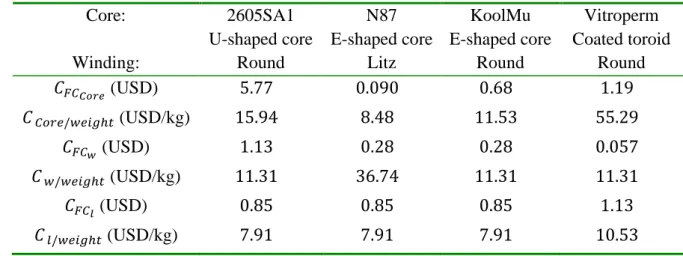
108 (4.60) where 𝐿 is the calculated inductance value, 𝐼𝑝𝑘 is the peak current, 𝐵𝑚 is the maximum operating flux density (𝐵𝑚 = 1.5𝑇), 𝐾𝑘 given as 𝑇𝑡 is a dimensionless constant, and the utilization factor is a dimensionless constant. 𝑠− 𝑇𝑎) is the temperature change between maximum surface temperature and maximum ambient temperature. Therefore, the core specification obtained from the manufacturer's database is presented in [184] as follows; effective cross section (𝐴𝑐), window winding area (𝑊𝑎), mean length turn (MLT), magnetic path length (MPL) and core volume (𝑉𝑐).
![Table 4.4: Core material properties [187]](https://thumb-ap.123doks.com/thumbv2/pubpdfnet/10366833.0/191.892.108.775.143.362/table-core-material-properties.webp)
Maximum Core Dissipation (𝑷 𝑪𝑫 )
Winding Design
Required Permeability (𝝁 𝒓 )
Peak Flux Density (𝑩 𝒑𝒌 )
Maximum Permeability (𝝁 𝒎𝒂𝒙 )
Core Loss
- Copper Loss
165 𝑃𝑓𝑒= 𝑉𝑐𝐾𝑐𝑓𝛼𝐵𝑐𝑚𝛽 (4.70) where 𝑉𝑐 is the core volume, 𝐾𝑐 is the loss coefficient, 𝑓 is the switching frequency, 𝛼 and 𝛽 are the Steinmetz empirical coefficients listed in [186].
Maximum Inductance (𝑳 𝒎𝒂𝒙 )
- Modulation and Voltage Balancing Control Technique
- Modulation Technique
- Voltage Balancing Control Technique
During the sweep mode, the boost mode of the converter topology is activated, the normal active mode (ie, mode 1) is inserted into the switching pattern without affecting the clamp capacitor voltage, as shown in Figure 4.13(b) . The duty cycle of the shoot-through mode (ST) (𝐷𝑠𝑡) is generated using the indirect dc-link control technique [177].
![Figure 1.2: Breakdown of the number of failures in various components of a WECS connected in an onshore Swedish WPPs [24]](https://thumb-ap.123doks.com/thumbv2/pubpdfnet/10366833.0/34.892.196.673.285.566/figure-breakdown-failures-various-components-connected-onshore-swedish.webp)
![Figure 1.3: Failure rate with the respective rated power capacity of WECS showing their operational years [24]](https://thumb-ap.123doks.com/thumbv2/pubpdfnet/10366833.0/34.892.133.756.699.980/figure-failure-respective-rated-power-capacity-showing-operational.webp)
![Figure 1.7: Breakdown of the failure rates and downtimes of electrical subsystem components of direct drive WECS [29]](https://thumb-ap.123doks.com/thumbv2/pubpdfnet/10366833.0/40.892.144.750.749.1036/figure-breakdown-failure-downtimes-electrical-subsystem-components-direct.webp)