NURASYIDAH BINTI MOHD SALLEH
This Report Is Submitted In Partial Fulfillment of Requirement for the Bachelor Degree of Electronic Engineering (Wireless Communication) With Honors
Faculty of Electronic and Computer Engineering Universiti Teknikal Malaysia Melaka
ACKNOWLEDGEMENT
I would like to express my deep gratitude and sincere appreciation to my supervisor Assoc. Professor Dr. Zahriladha bin Zakaria for encouragement and valuable guidance and critic towards this project. I am also indebted to Universiti Teknikal Malaysia Melaka (UTeM) in completing my project with all laboratory facilities
In completing this thesis, I had worked with many academicians, seniors, friends, and laboratory technician. They have helped me toward my understanding, thoughts and support. Special thanks to my parents and family with their continuous inspiration and love. Last but not least, many thanks to my panels for the project presentation that has improved my presentation skills by their comments and tips.
ABSTRACT
ABSTRAK
TABLE OF CONTENTS
CHAPTER TITLE PAGE
PROJECT TITLE i
REPORT VERIFICATION STATUS FORM ii
DECLARATION iii
SUPERVISOR DECLARATION iv
DEDICATION v
ACKNOWLEDGEMENT vi
ABSTRAK vii
ABSTRACT viii
TABLE OF CONTENT ix
LIST OF TABLES xiii
LIST OF FIGURES xv
LIST OF ABBREAVIATION xvi
LIST OF APPENDICES xii
1 INTRODUCTION 1
1.1 Research Background 1
1.2 Problem Statement 3
1.3 Objectives 4
1.4 Scope of Project 4
1.5 Project Planning 5
2 LITERATURE REVIEW 8
2.1 Introduction 8
2.2 Impedance Matching 9
2.2.1 Single stub Matching 9
2.2.2 Double stub Matching 10
2.3 Voltage Doubler 11
2.4 Diode 12
2.5 Load Resisitor 15
2.6 Power Combiner 16
2.7 Harmonic Balance Simulator 17
2.8 Efficiency 18
2.9 Microstrip design 19
2.9 Literatue Summaryuit 21
3 PROJECT METHODOLOGY 23
3.1 Introduction 24
3.2 Matching Network 25
3.3 Wilkinson Power Combiner 27
3.4 Lumped Element Design 29
3.5 Interdigital Capacitor 30
3.6 LineCalc Tools 33
3.7 Tuning and Optimization 34
3.8 Design Layout 35
4 RESULT AND DISCUSSION 40
4.1 Introduction 41
4.2 Choices of Diode 40
4.3 Choice of Load 42
4.4 Matching Network 46
4.5 Wilkinson Power Combiner 48
4.6 Simulation Results 50
4.7 Experimental Results 53
5 CONCLUSION AND SUGGESTION 57
5.1 Conclusion 57
5.2 Future Work 58
REFERENCES 59
LIST OF TABLES
NO TITLE PAGE
2.1 SPICE Parameter 15
3.1 Parameter of Interdigital capacitor 31
3.2 Parameter FR4 board 35
4.1 Output voltage of frequency 2.4GHz for voltage doubler 42 with diodes HSMS 286B
4.2 Output voltage of frequency 1.8 GHz for voltage doubler 44 with diodes HSMS 286B
4.3 Efficiency of dual band rectifying circuit 50
4.4 Output voltage for single frequency rectifier circuit 51 dual band frequency rectifier circuit
LIST OF FIGURES
NO TITLE PAGE
1.1 Block diagram of RF energy scavenging 3 1.2 Gantt chart of project planning 5 2.1 Single stub circuit: shunt stub and series stub. 9
2.2 Double-stub tuning 11
2.3 Basic rectifier and voltage doubler 12
2.4 VI characteristic curve 14
2.5 Equivalent linear circuit diode chip 14
2.6 Wilkinson Power Combiner 17
2.7 Harmonic balance simulation 18
2.8 Rectifier structure 19
2.9 Microstrip line and electric feed line 21 3.1 Project Methodology flow chart 25
3.2 Single stub for frequency 2.45 GHz 26
3.3 Single stub for frequency 1.8 GHz 27 3.4 Double stub for frequency 2.45 GHz 27 3.5 Double stub for frequency 1.8 GHz 27 3.6 Single stage Wilkinson power combiner 28
3.7 Double stage Wilkinson power combiner 28
3.8 Lumped element circuit of voltage doubler 29
3.9 Interdigital capacitor structure and symbol 30
3.10 Interdigital capacitor in voltage doubler circuit 31
3.12 Tuning layout in ADS 33
3.13 Comparison result before and after tuning the circuit 33
3.14 Circuit design for dual band rectifying circuit 34
3.15 Specification FR4 substrate 35
3.16 Layout design by momentum 35
3.17 Fabricated rectifier circuit 36
3.18 The arrangement to find the output voltage of the rectifier circuit 37
4.1 Output voltage of the rectifier with different diode 40
4.2 Output voltage of difference load for voltage doubler at 41
frequency 2.45GHZ 4.3 Efficiency of voltage doubler circuit with difference loads at 43
frequency 2.45 GHz 4.4 Output voltage of difference load for voltage doubler at 43
frequency 1.8 GHZ 4.5 Efficiency of voltage doubler circuit with difference loads at 45
frequency 1.8 GHz 4.6 Single stub matching network for 2.4GHz 45
4.7 Single stub matching network for 1.8 GHz 46
4.8 Comparison of single stub, double stub and circuit without a stub 47
4.9 The comparison between single and multistage Wilkinson 48
power combiner 4.10 Dual band rectifying circuit for RF energy scavenging 50
4.11 Output voltage for single frequency and dual frequency 51
4.12 Rectifier measurement with LED as a load 54
LIST OF ABBREVIATION
AC - Alternating Current ADS - Advance Design System DC - Direct Current
EM - Electromagnatic FR4 - Flame Retardant 4
GSM - Global System for Mobile HB - Harmonic Balance
ISM - Industrial Scientific and Medical RC - Resisitance Capacitance
RF - Radio Frequency
LIST OF APPENDICES
CHAPTER 1
INTRODUCTION
1.1 Research Background
With the growing technologies of integrated circuits towards low power consumption and low voltage, energy scavenging has been a fast growing topic. Energy scavenger is the process by which energy is derived from ambient sources and converted into suitable direct current (DC) power for wireless application such as sensor network, portable medical devices and radio frequency identification (RFID) tags. The developing in this technology can potentially be used to reduce or eliminate the dependence most wireless applications and low power integrated technology have on wire or non-autonomous power sources.
identified by researchers as alternative energy. Energy scavenging from a solar cell or photovoltaic cell is where it converts the light energy into thermal and uses mechanical heat to generate electricity. A human body also can be one of the sources for energy scavenging. Electrical energy can be generated by walking, jogging and cycling [1]. Electromagnetic energy scavenging refers to the Faraday’s electromagnetic induction theory. An oscillating coil in the magnetic field produces a voltage. The voltage or electromagnetic force (EMF) is proportional to the change of magnetic field or flux.[2] Radio frequency (RF) has been a hot topic in energy scavenging because of its availability and easy scavenging system. [3]
Rapid grow of the telecommunication technologies leads to plenty numbers of RF power sources which propagate electromagnetic wave to the air such as wireless local network (WLAN) routers, cellular base station and TV and radio broadcasting towers. RF signals are abundant and always available in ambience and become essentially free power resources [4]. RF waves exist in almost populated areas that they are present at all the time and it can come out with a smaller size as it only required part of an antenna.
Figure 1.1 shows the basic block diagram of RF energy scavenging. The antenna is used to capture RF source that is coming from several sources such as WIFI, base station and satellite communication. Matching circuit that consists of lumped element, such as capacitor and inductor is giving a good impedance matching at the output antenna for different frequencies. Rectifier circuit will act as a conversion of RF energy to DC power. Voltage doubler will increase the voltage level that will use for charging or storing. In the rectifier circuit, efficiency is very important to define the ratio if DC power delivered to the load. To achieve high conversion efficiency, the usage of multiple frequency bands, antenna arrays, dual-circularly polarized patch antenna, etc. have been developed [7].
Figure 1.1: Block diagram of RF energy scavenging [8]
1.2 Problem Statement
but it should be noted that solar power suffers from energy shortage during night times. RF Energy scavenging varies with time and space.
In this thesis, it will focus on the designing of dual band rectifying circuit for RF energy scavenging. In this project, it will focus on frequency of 2.45 GHz and 1.8 GHz. The 2.45 GHz is Industrial Scientific and Medical (ISM) and its presence in the WI-FI networks while 1.8GHz presence in the Global System for Mobile (GSM) band that corresponding on mobile telephone systems.
There is researches done in designing a dual band rectifier such as [4]. In [4] although the rectifier can operate at 2.1 GHz and 2.45 GHz, it operates on a single frequency at a time. In this project, dual frequency input can operate simultaneously. This project a little bit complicated. The used of power combiner tests in this project to combine the dual band frequency.
1.3 Objectives
The objective of this project is to study and analyze the behavior of impedance matching, power combiner and rectifier circuit. This project also focuses on design, simulate and fabricate dual band energy scavenging that can operate at frequency 2.45 GHz and 1.8 GHz.
1.4 Scope of Project
can be gathered from journals, books and also paperwork on the internet. In this project the dual frequency is combined by using Wilkinson power combiner.
This project also focuses on designing a rectifier circuit that will convert RF energy to DC power. The proposed frequency of this project is 1.8GHz and 2.45GHz. One of the elements of rectifier circuit is a selection of diodes. A diode with fast switching time is important in order to achieve high efficiency. For the impedance matching network, single stub matching network is designed for the individual frequency. The performance of the rectifier circuit also influences by the load resistor. Several values of loads are analyzed to give the best performance for the circuit. To design and simulate all the circuits, Advance Design System (ADS 2011) is chosen which use the Harmonic Balance as simulation method. After all the circuit design is completed, the circuit will be fabricated and performance of the circuit will be measured in the laboratory by using signal generator.
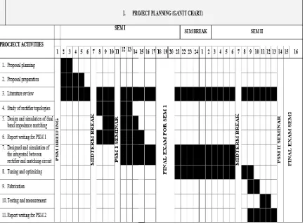
1.5 Project Planning
Figure 1.2: Gantt chart of project planning
1.6 Overview of Thesis Organization
There are five chapters in this thesis organized as a fellow:
In chapter 2, the theoretical background of rectifier circuit and matching network, Schottky diode and also Wilkinson power combiner is briefly explained as its use in rectifier circuit. Relevant work also presented.
Chapter 3 focuses on methodology for this project. This chapter will shows the calculation part of impedance matching and the Wilkinson power combiner. The transformation of lumped element to transmission line also will explain briefly. Fabrication and measurement part also will explain in this chapter
Chapter 4 focuses on the result of simulation rectifier. The measurement will compared with simulation results. The result and finding are discussed. The setup used for RF measurement is also introduced.
CHAPTER 2
LITERATURE REVIEW
2.1 Introduction
Rectification process is obtained by the conversion of input RF power into DC power supply. Elements in rectifier circuit consist of impedance matching circuit, Schottky diode, and also power combiner to combine the dual frequency. The conversion of RF to DC efficiency is transformed by losses of impedance matching circuit and diodes. The nonlinear components of rectifying circuits such as diode will produce harmonics of the fundamental frequency.
2.2 Impedance Matching
The critical part of matching network is to lessen the transmission loss from an antenna to a rectifier circuit and increase the input voltage of a rectifier circuit. As a result, a matching network is typically made with reactive components such as coils and capacitors that are not dissipative. Maximum power transfer can be realized when the impedance at the antenna output and the impedance of the load are conjugates of each other. This procedure is known as impedance matching [6].
The function impedance matching circuit is to provide maximum power transfer to the load of the RF power from the source. The design of matching networks for multi-band or broadband operation of the rectifier is important to send maximum power from the source to rectifying device. The standard RF source impedance is considered 50Ω.[2]
2.2.1 Single Stub Matching
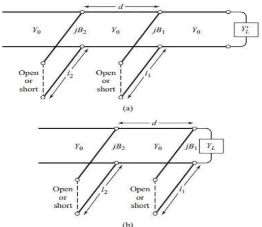
One of matching technique uses a single open circuited or open circuited length of stub connected either in parallel or in series with the transmission feed line at a certain distance from the load [10]. In single-stub tuning, the two variable parameters are the distance, d, from the load to the stub position, and the value of susceptance or reactance of the stub. For the shunt-stub case, the basic idea is to select d so that the admittance, Y, seen looking into the line at distance d from the load is of the form Y0 + j B. Then the stub susceptance is chosen as − j B, resulting in a matched condition.
In a transmission line, shunt open circuit are easier to fabricate because it doesn’t need the ground plane. Figure 2.1 shows the shunt and series single stub.
Figure 2.1: Single stub circuit (a) shunt stub (b) series stub [10]
2.2.2 Double Stub Matching
Figure 2.2: Double-stub tuning. (a) Original circuit with the load an random distance from the first stub. (b) The equivalent circuit with the load
transformed to the first stub.[10]
![Figure 1.1: Block diagram of RF energy scavenging [8]](https://thumb-ap.123doks.com/thumbv2/123dok/499552.56000/16.612.110.467.284.415/figure-block-diagram-rf-energy-scavenging.webp)
![Figure 2.1: Single stub circuit (a) shunt stub (b) series stub [10]](https://thumb-ap.123doks.com/thumbv2/123dok/499552.56000/23.612.249.435.154.399/figure-single-stub-circuit-shunt-stub-series-stub.webp)