DESIGN A DUALBAND RECTIFYING CIRCUIT FOR RF POWER TRANSFER
MOHAMAD AZLI ZHAFRI B MD GUZALI
This Report Is Submitted in Partial Fulfillment of Requirement for the Degree in Electronic Engineering (Industry Electronics)
With Honors
Fakulti Kejuruteraan Elektronik dan Kejuruteraan Komputer Universiti Teknikal Malaysia Melaka
v
DEDICATIONS
To Allah The Almighty
I devoted my life and death to You, Allah. May my life be within Your guidance.
To My Parents
Thank you for your sacrifice and love till the end of your life. Your souls have always remained forever in my heart. No such compensation except Allah.
To My Supervisor and Lecturer
Thank you for all the knowledge and support. Your support, patience, and encouragement give me strength throughout the whole course.
To My Seniors
Nasrullah B Saifullah and Sharif Ahmed Qasem Ahmed
Thanks a lot for your help and kindness.
To All Friends
vi
ACKNOWLEDGEMENT
Firstly, I would like to express my grateful to the God for the good health and wellbeing that were necessary to complete this book
I would like to extend my deepest gratitude to my supervisor Associate Professor Dr. Zahriladha B Zakaria for his unwavering support, collegiality, and mentorship throughout this project.
I placed on record, my sincere thanks, to Dr. Nurul Fajar B Abd Manap, Dean for the Faculty for the continuous encouragement. In addition, I am also grateful to Mr. Imran and Mr. Aini for providing me with all necessary facilities for the research.
vii
ABSTRACT
viii
ABSTRAK
ix
LIST OF ABBREVIATIONS AND ACRONYMS xv
LIST OF APPENDICES xvi
x
2 LITERATURE REVIEW
2.1 Introduction 10-12
2.2 Rectifying Circuit 13
2.3 Voltage Multiplier 14-15
2.4 Diode for Rectifying Circuit 16
2.5 Power Combiner 17-19
2.6 Filter 19-21
2.7 Matching Network 21-22
3 RESEARCH METHODOLOGY
3.1 Introduction 23-24
3.2 Define specification of dual band rectifying power transfer
25
3.3 Rectifier circuit 25-26
3.3.1 Lumped Element Design. 26-27
3.3.2 Microstrip line design for rectifier circuit 28-29
3.4 Power Combiner Design 29
3.4.1 Wilkinson Power Combiner Calculation 29-30 3.4.2 Wilkinson Power Combiner Circuit using ADS 31-32
3.5 Tuning and Optimization 33-34
3.6 Layout Design 34-35
3.7 Fabrication and Measuring 35-36
4 RESULT AND DISCUSSION
4.1 Introduction 37
4.2 Simulation result 37
4.2.1 Wilkinson Power Combiner 37-38
4.2.2 Simulation for Rectifier circuit. 39-41 4.2.3 Simulation for Dual band rectifying circuit for the
different resistor.
42
4.2.4 Simulation for dual band rectifier circuit for different Schottky diode
43
xi
4.3 Experimental result for dual band rectifying circuit 45-48 4.4 Efficiency of Dual band rectifying circuit 49
4.5 Discussion 50-51
5 CONCLUSION AND RECOMMENDATION
5.1 Introduction 52
5.2 Conclusion 52
5.3 Suggestion for future network. 53
REFERENCES 54-56
xii
LIST OF TABLES
TABLE TITLE PAGE
Table 1.1 Energy harvesting source 2
Table 1.5 Gantt chart of the project 7
Table 2.1 Summary of the literature reviews 11-12
xiii
LIST OF FIGURES
FIGURE TITLE PAGE
Figure 1.1 Block diagram of RF energy harvesting system 3
Figure 2.2.1 Structure of rectifier 13
Figure 2.3.1 Topologies of Greinacher Voltage Doubler 14 Figure 2.3.2 Villard Multiplier and (b) Dickson Multiplier 14
Figure 2.3.3 Cascade Villard Doubler Circuit 15
Figure 2.4.1 Schottky Diode operating voltage 17
Figure 2.5.1 Topology of ideal Wilkinson power divider, (b) Parameter response for ideal Wilkinson power divider
18
Figure 2.5.2 Lumped equivalent for Wilkinson power divider circuit. 18 Figure 2.6.1 Response graph for different types of filter 20 Figure 2.6.2 Topology of single band RF filter for RF harvester and
response of bandpass filter
20
Figure 2.6.3 Topology for multiband RF harvester with RF filter 21
Figure 2.7.1 Concept of matching network 21
Figure 2.7.2 Single stub matching circuit 22
Figure 3.1.1 Block diagram for the project 23
Figure 3.1.2 Flow chart of the project 24
Figure 3.3.1 Voltage doubler rectifier circuit 25
Figure 3.3.1.1 Lumped elements for rectifier circuit 26 Figure 3.3.1.2 Simulation parameter for simulation purpose 27
Figure 3.3.1.3 RF-DC conversion graph 27
xiv
Figure 3.3.2.2 Basic structure of interdigital capacitor 29
Figure 3.4.1 Wilkinson power combiner circuit. 29
Figure 3.4.1.1 Multistage Wilkinson power combiner 30 Figure 3.4.1.2 Wilkinson Power combiner calculation using Excel
software
30
Figure 3.4.2.1 Line calculation for width and length of Z0 31
Figure 3.4.2.2 Wilkinson Power Combiner circuit 32
Figure 3.4.2.3 Wilkinson response 32
Figure 3.5.1 Dual Band Rectifier with Wilkinson Power Combiner circuit
33
Figure 3.5.2 Tuning parameter tool in ADS 33
Figure 3.5.3 RF-DC conversion result before and after tuning process 34 Figure 3.6.1 Layout design of rectifying circuit 34
Figure 3.6.2 Substrate setting 35
Figure 3.7.2 Steps for PCB etching process 35
Figure 3.7.3 Dual band rectifier circuit 36
Figure 3.7.4 The arrangement during measurement process 36
Figure 4.2.1.1 Wilkinson Power Combiner Circuit 38
Figure 4.2.1.2 Wilkinson power combiner response 38
Figure 4.2.2.1 Rectifier circuit 40
Figure 4.2.2.2 RF-DC conversion for 1.8GHz input frequency 40 Figure 4.2.2.3 RF_DC conversion for 2.45GHz input frequency 41 Figure 4.2.3.1 RF-DC conversion with the different selective resistor 42 Figure 4.2.4.1 RF-DC conversion output with different Schottky diode 43 Figure 4.2.5.1 RF-DC conversion for dual band rectifying circuit 44
Figure 4.3.1 Graph for Voltage Vs Input Frequency for RF-DC conversion
47
Figure 4.3.2 Graph for Voltage against RF_power for RF-DC conversion
48
xv
LIST OF ABBREVIATIONS AND ACRONYMS
RF Radio Frequency
DC Direct Current
ADS Advance Design System
FR4 Flame Retardant 4
WPT Wireless Power Transmission
AC Alternating Current
xvi
LIST OF APPENDICES
APPENDIX TITLE PAGE
Appendix A Data sheet of Diode HSMS2860 57-62
Appendix B FR 4 63
CHAPTER 1
INTRODUCTION
1.1 Project Overview
Nowadays, energy harvesting has been a popular topic among the researchers, especially in the wireless communication field. The first concept of wireless energy transmission who is invented by Nikola Tesla in 1890 has been developed by researchers so that it can be applied in many applications. Normally, an active device like the battery is used to inject power into a circuit due it capability to produce an energy in the form of voltage or current. Since the battery has a life span, an unlimited power source is needed to replace the battery due to its limitation. The passive power device is introduced because this device can extract their power from unlimited sources such propagating radio waves or other forms without requiring any internal power sources.
2
operating in multiple bands. At the end, this system can apply in any places as long there is the available frequency in that area.
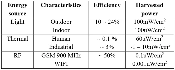
Even RF energy is an unlimited source obviously, but it most limited source in term of power density, for example, RF (0.01~0.1W/cm2), photovoltaic
(10W/cm2~10mW/cm2) and thermal (10W/cm2~10mW/cm2) [1].
Table 1.1: Energy harvesting source
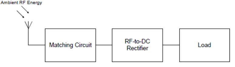
RF energy harvesting is a process that converts a suitable DC power from an unlimited source such an ambient RF energy. The main element of the RF energy harvesting system is shown in Figure 1.1. Matching circuit consist of the conductive and inductive element to ensure the maximum input power delivery from the antenna to rectifier [2]. A good matching circuit depends on its capability to deliver maximum input
power to the rectifying circuit. The challenges task to design dual band rectifier is to match the rectifier with a two frequency band and at the same time minimize the sensitivity of rectifier [3]. Rectenna are the combination of rectifier and antenna that was initially
designed by W. C. Brown for converting the microwave power into direct current DC power [4], [5]. Rectenna is the key block of the front end receiving a portion of a wireless
3
Figure 1.1: Block diagram of RF energy harvesting system
One of application is a rechargeable circuit. By applying this system to the rechargeable circuit, it’s capable of extending the life of battery beside can replace the battery as an input source of the circuit. At the same time, the circuit becomes maintenance free. As long as the circuit is placed in available frequency area, the circuit will operate normally.
1.3 Problem statement
4
One of the factor that effect of RF-DC conversion is source power. The power density of ambient RF energy is very small and this is a challenging task to design a very high-efficiency RF-DC conversion. In order to overcome that problem, an efficient rectifier circuit is needed to provide high-efficiency RF-DC power conversion. The designed rectifier should be able to operate at multiband of frequency for obtaining the high power DC power for the end device [6]. Single band rectifier only can capture for
one RF signal at once. Normally, a single band rectifier circuit is not enough to produce a good performance of RF-DC conversion due to its limitation of power density. By designed multiband rectifier circuit, it can increase power delivery from source to rectifier because multiband rectifier can cover various frequencies. The Even multiband rectifier can cover various frequencies, but, designing multiband rectifier is not easy. The difficult part is to match the rectifier for more than one frequency bands at the same time minimize the sensitivity of the rectifier. Maximum power delivery can be obtained by design matching network for rectifying circuit [3]
1.3 Objectives
The main objective of this project is to develop high efficiency and low power consumption of RF-DC conversion for the dual band rectifying circuit in RF energy harvesting system. In addition, the sub-objectives are stated as follow:
To design a dual-band rectifying circuit which operates at 1.8 GHz and 2.45 GHz with a good matching circuit.
5
1.4 Scope of project
Then the main objective of this project is to design a dual-band rectifying circuit which can operate at 1.8 GHz and 2.45 GHz with a good matching circuit. All related information from various resources like the internet for this project is gathering to be as guidelines to accomplish this project followed the time given.
This project is focused on design and analysis a dual band rectifier that can operate at different frequencies with a good matching circuit. In order to improve the efficiency of the RF energy harvesting system, power combiner, and filter design is adding on the rectifier circuit. The design process of the rectifier circuit can be formed by using Agilent Advance Design System (ADS 2011). ADS software can analyze the initial design of the dual band rectifier system in term of performance before proceed to the next process which is fabrication process.
The dual band rectifier is a combination of two single bands which operate at different frequencies 1.8GHz and 2.45GHz. A single band rectifier is designed and analyze for both frequencies before combining it into a dual band rectifier circuit. A good performance of diode need to be selected, otherwise, it will affect the performance of the rectifier. Since the circuit operates at high frequencies, harmonic frequencies will occur. The dual bandpass filter will be designed to overcome harmonic frequencies problem. Then, power combiner is designed to separate the operating frequencies of the rectifier and deliver an optimum input power that captured from an ambient environment. Next process is matching network design.
6
1.5 Methodology
1.5.1 Project Planning
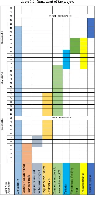
Project planning is one of the element to ensure the project is finished within the prescribed time with well-planned and organized. There are a lot of sub-activities to make a complete project and its will described by using Gantt chart. Gantt chart will manage each activity with a specific duration time so that project will be finished on time. Figure 1.5.1 shows the Gantt chart of the project.
1.5.3 Data Collection
7
8
1.6 Contribution
The project outcome is as follows:
a. A dual band rectifying circuit for RF energy harvesting is designed. This RF energy harvesting can operate at two different frequencies and provide a high performance of RF-DC conversion.
b. An optimum technique can implement on proposed rectifier to achieve an efficient RF-DC conversion performance for further research.
c. DC-DC converter can be implemented at the output of rectifier as a stabilizer to smooth the output DC value.
d. This project has an opportunity to be commercialized if further research is continued to obtain high performance of RF-DC conversion.
1.7 Organization of thesis
This thesis is organized as follows:
1. Chapter 1 describes the overall thesis in general and leads the reader to the problem statement of the project. Objective and scope of project are defined as well as project methodology to ensure project well organized besides achieve project objectives