www.ijsret.org
764 International Journal of Scientific Research Engineering & Technology (IJSRET), ISSN 2278 – 0882
Volume 3, Issue 4, July 2014
Design Consideration of N-Drift Region Doping Concentration
In High Voltage VDMOS Transistor
H.H.M. Yusof1, Wijaya Bayu Murti2, N. Soin3
1
Department of Industrial Electronics, FKEKK, UTeM, Malaysia Email: [email protected]
2 Department of Electrical Engineering, UM, Malaysia
Email: [email protected]
3
Department of Electrical Engineering, UM, Malaysia Email: [email protected]
ABSTRACT
N-drift doping concentration has important contribution in determining the breakdown voltage and on-resistance of the device. It should be well considered because higher N- drift doping concentration can minimize the on-resistance of the device, but also lowering breakdown voltage of the device that expected to be high. It also has a proportional relationship with threshold voltage degradation caused by hot carrier injection. So the variation of N-drift doping concentration can be used to optimize the VDMOS transistor performance.
Keywords– VDMOS, breakdown voltage, on-resistance, hot carrier injection, HCI
I.
INTRODUCTION
The fabrication processing parameters are important in determining the performance of the device. In VDMOS transistor the N-drift doping concentration has high influence for determining on-resistance breakdown voltage and threshold voltage degradation caused by hot carrier injection.In the structure of VDMOS transistor the N-drift region is located above the substrate region of the device, as shown in Fig. 1.
The general expectation of high voltage VDMOS transistor is to have high breakdown voltage, lower degradation due to hot carrier injection and low on-resistance. The break down voltage of a device will determine the capability of the device to withstand certain maximum voltage value that the device will work normally.
Fig. 1: Cross-sectional view of VDMOS structure [1]
The on-resistance of power MOSFET will define the speed of the switching capability (switching frequency). And the degradation due to hot carrier effect will determine performance stability of the device and also the lifetime of the device.
II.
EXPERIMENT PARAMETER
A. On-Resistance
www.ijsret.org
765 International Journal of Scientific Research Engineering & Technology (IJSRET), ISSN 2278 – 0882
Volume 3, Issue 4, July 2014
This internal resistance is called as on-resistance, it is defined as the total resistance to current flow from source electrode to drain electrode during voltage applied to gate electrode to make the device in on condition. Every layer of different materials and different doping concentrations in the VDMOS structure contributes a different resistance toward the total on-resistance [1].
The resistance becomes higher in N- drift region area because the current flow entering N- drift region area is spreading and the cross-sectional width become bigger compare the width of the JFET region. The current proportional relation with the doping concentration of N-drift region.
B. Breakdown Voltage
Breakdown voltage of VDMOS structure is defined by the drain voltage required for current to flow in the device without the presence of gate voltage. The VDMOS transistor should capable of handling high voltage, thus the desired breakdown voltage should be chosen properly during designing the device.
The breakdown voltage is directly influenced by the doping concentration of the N- drift region (ND) and the
thickness of N- drift region (tD). From the desired
breakdown voltage the N- drift region doping concentration (ND) can be calculated as in equation [1] :
(2)
And the N- drift region thickness (tD) can be calculated
from the desired breakdown voltage (BV) and the N- drift region doping concentration as in equation [1]:
(3)
where εs is the permittivity of the silicon, and q is the
electron charge.
The ideal on-resistance based on the breakdown voltage (BV) of the VDMOS transistor can be calculated by equation [2]:
(4)
Wpp is the width of the parallel-plane depletion during
breakdown, condition when current flowing even though no gate voltage applied.
C. Hot Carrier Injection
The effect of the hot carrier injection can be check on the threshold voltage degradation of the device [3]. The simulation of threshold voltage degradation caused by hot carrier injection can be used to determine the expected lifetime of the device.
The N-drift region doping concentration has a relation with the threshold voltage degradation caused by hot carrier injection. In the following part it will be shown that this investigation should be considered when optimizing the VDMOS transistor by varying the doping concentration of N-drift region.
III.
RESULTS AND ANALYSIS
Simulations are done by using SILVACO software. The VDMOS transistor structure is virtually fabricated using ATHENA and the device characteristics are simulated using ATLAS.
This research done by varying the doping concentration of N-drift region, and analyze the result based on the breakdown voltage and the threshold voltage degradation caused by hot carrier injection.
The impurity used for N-drift region is phosphorus. The variation of doping concentration is based on paper by Maizan [4].
www.ijsret.org
766 International Journal of Scientific Research Engineering & Technology (IJSRET), ISSN 2278 – 0882
Volume 3, Issue 4, July 2014
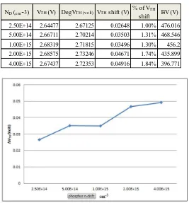
Table 1: Simulation Results extracted from SILVACO
ND (c m-3) VTH (V) DegVTH (vo lt) VTH shift (V) % of VTH shift BV (V) 2.50E+14 2.64477 2.67125 0.02648 1.00% 476.016 5.00E+14 2.66711 2.70214 0.03503 1.31% 468.546
1.00E+15 2.68319 2.71815 0.03496 1.30% 456.2 2.00E+15 2.68575 2.73246 0.04671 1.74% 435.899 4.00E+15 2.67437 2.72353 0.04916 1.84% 396.771
Fig. 2: Plotted graph of ND / VTH shift
Fig. 3: Plotted graph of ND / BV
The simulations are done in 5 set of doping concentrations, the default value is the 1 x 1015 cm-3. The second column in Table 1 shows the threshold voltage of the device, the third column shows the threshold voltage of the device after hot carrier injection stress test.
Fig. 2 shows the graph for the shift of threshold voltage. From the graph, it shows that the threshold voltage is shifted along the incremental of the doping concentration of N-drift region due to hot harrier injection, and it can be said that the doping concentration of N-drift doping region has proportional relation toward the threshold voltage degradation caused by HCI. Fig. 3 shows the graph for breakdown voltage of the device (BV). It shows that the doping concentration of N-drift region has inversely proportional relation with the breakdown voltage. From these two results, it shows the contradictive consideration in deciding the doping concentration of the N-drift region. Additionally the influence toward the internal resistance also, which is as in equation (1), higher the doping concentration of N-drift region, the internal resistance will become smaller.
IV.
CONCLUSION
In designing high voltage VDMOS transistor, the doping concentration of N-drift region should be well considered, since it highly influence the breakdown voltage, internal resistance, and the degradation caused by hot carrier injection. The application specification of the device should be well understood, to help the designing of the device and to get the optimum performance toward the application.
V.
ACKNOWLEDGEMENT
The authors are grateful to Universiti Teknikal Malaysia Melaka because this work is financially supported by the university under PJP grant scheme
(No: PJP/2013/FKEKK(31B)/S01221).
VI.
REFERENCES
[1] Baliga, B.J. 2010. Advance Power MOSFETs Concepts. New York: Springer.
[2] Baliga, B.J. 2008. Fundamentals of Power Semiconductor Devices. New York: Springer.
[3] Eiji Takeda, C. Y. Y., Akemi Miura-Hamada.1995. Hot-Carrier Effects in MOS Devices. San Diego, California: Academic Press.
![Fig. 1: Cross-sectional view of VDMOS structure [1]](https://thumb-ap.123doks.com/thumbv2/123dok/514470.58619/1.612.329.581.224.424/fig-cross-sectional-view-vdmos-structure.webp)