__________________________________________________________________________________________
DYNAMIC MODEL OF ZETA CONVERTER WITH FULL-STATE
FEEDBACK CONTROLLER IMPLEMENTATION
Hafez Sarkawi
1, Mohd Hafiz Jali
2, Tarmizi Ahmad Izzuddin
3, Mahidzal Dahari
41
Lecturer, Faculty of Electronics and Computer Engineering (FKEKK), University Teknikal Malaysia Melaka (UTeM),
Melaka, Malaysia, [email protected]
2, 3
Lecturer,
4Senior Lecturer, Faculty of Electrical Engineering (FKE), University Teknikal Malaysia Melaka (UTeM),
Melaka, Malaysia, [email protected], [email protected], [email protected]
Abstract
Zeta converter is a fourth order dc-dc converter that can increases (step-up) or decreases (step-down) the input voltage. By considering dynamic model of the converter, the accuracy of the converter’s modeling and simulation are increased thus make it easier to produce the hardware version of the converter. State-space approach is a time-domain method for modeling, analyzing, and designing a wide range of systems which can be described by differential equations or difference equations. This gives great advantages because it particularly suited for digital computer implementation for their time-domain approach and vector-matrix description. The converter needs feedback control to regulate its output voltage. This paper presents the dynamic model of zeta converter. The converter is modeled using state-space averaging (SSA) technique. Full-state feedback controller is implemented on the converter to regulate the output voltage. The simulation results are presented to verify the accuracy of the modeling and the steady-state performance subjected to input and load disturbances.
Index Terms: Modeling, Zeta converter, SSA technique, Full-state feedback controller
---***---
1. INTRODUCTION
Nowadays, dc-dc converter is widely used as a power supply in electronic system. In the battery-operated portable devices, when not connected to the AC mains, the battery provides an input voltage to the converter, which then converts it into the output voltage suitable for use by the electronic load. The battery voltage can vary over a wide range, depending on a charge level. At the low charge level, it may drop below the load voltage. Hence, to continue supplying the constant load voltage over the entire battery voltage range, the converter must be able to work in both buck and boost modes. The dc-dc converters that meet this operational requirement are buck-boost, Cuk, sepic, and zeta converters. For this paper, zeta converter is selected because it has given the least attention. Zeta converter is fourth order dc-dc converters that can step-up or step-down the input voltage. The converter is made step-up of two inductors and two capacitors. Modeling plays an important role to provide an inside view of the converter’s behavior. Besides that, it provides information for the design of the compensator. The most common modeling method for the converter is state-space averaging technique (SSA). It provides a systematic way to model the converter which is a matrix-based technique. This state-space approach is a time-domain model where the system is described by differential or difference equation. It allows greatly simplified mathematical representation of the systems which is vector-matrix differential equation. This poses great advantage because it
particularly suited for digital computer implementation due to their time-domain approach and vector matrix description.
Open-loop system has some disadvantages where the output cannot be compensated or controlled if there is variation or disturbance at the input. For the case of zeta converter, the changes in the input voltage and/or the load current will cause the converter’s output voltage to deviate from desired value. This is a disadvantage because when the converter is used as power supply in electronic system, problem could be happened in such that it could harm other sensitive electronic parts that consume the power supply. To overcome this problem, a closed-loop system is required. The existence of this feedback loop along with the controller would enable the control and regulation of the output voltage to the desirable value.
2. OVERVIEW OF SSA TECHNIQUE
State-space averaging (SSA) is a well-known method used in modeling switching converters [1]. For a system with a single switching component with a nominal duty cycle, a model may be developed by determining the state and measurement equations for each of the two switch states, then calculating a weighted average of the two sets of equations using the nominal values of the time spent in each state as the weights. To develop the state space averaged model, the equations for the rate of inductor current change along with the equations for the rate of capacitor voltage change that are used.
A state variable description of a system is written as follow:
Bu Ax x′= +
Eu Cx vO= +
Where A is n x n matrix, B is n x m matrix, C is m x n matrix
and E is m x m matrix. Take note that capital letter E is used
instead of commonly used capital letter D. This is because D
is reserved to represent duty cycle ratio (commonly used in power electronics).
For a system that has a two switch topologies, the state equations can be describe as [2]:
Switch closed
u B x A x′= 1 + 1
u E x C vO= 1 + 1 Switch open
u B x A x′= 2 + 2
u E x C vO= 2 + 2
For switch closed for the time dT and open for (1-d)T, the
weighted average of the equations are:
( )
[
Ad A d]
x[
Bd B( )
d]
u x′= 1 + 21− + 1 + 21−(
)
[
Cd C d]
x[
Ed E(
d)
]
u vO= 1 + 21− + 1 + 21−By assuming that the variables are changed around steady-state operating point (linear signal), the variables can now be written as:
O O
O V v
v
u U u
d D d
x X x
~ ~
~ ~
+ =
+ =
+ =
+ =
Where X, D, and U represent steady-state values, and x͂, d͂, and
ũ represent small signal values.
During steady-state, the derivatives (x’) and the small signal
values are zeros. Equation (1) can now be written as:
BU AX + =
0
BU A X=− −1
While Equation (2) can be written as:
EU BU CA
VO =− +
−1
The matrices are weighted averages as:
(
)
(
)
(
D)
C D C CD B D B B
D A D A A
− + =
− + =
− + =
1 1 1
2 1
2 1
2 1
For the small signal analysis, the derivatives of the steady-state component are zero:
x x x
X
x′= ′+ ~′= 0+ ~′= ~′
Substituting steady-state and small signal quantities in Equation (5) into Equation (3), the equation can be written as:
(
)
(
(
)
)
[
A D d A D d]
(X x)[
B(
D d)
B(
(
D d)
)
]
(U u)x ~ 1 ~ ~ ~ 1 ~ ~
~
2 1
2
1 + + − + + + + + − + +
= ′
If the products of small signal terms x͂d͂ can be neglected, the
equation can be written as:
( )
[AD A D]x [BD B( D)]u [(A A)X (B B )U]d
x 1 ~ 1 ~ ~
~
2 1 2 1 2
1 2
1 + − + + − + − + −
= ′
or in simplified form,
(
)
(
)
[
A A X B B U]
d uB x A
x ~ ~ ~
~
2 1 2
1− + −
+ + = ′
Similarly, the output from Equation (4) can be written as:
( )
[
Cd C d]
x[
Ed E( )
d]
u[
(
C C) (
X E E)
U]
d vO~ ~
1 ~
1 ~
2 1 2 1 2
1 2
1 + − + + − + − + −
=
or in simplified form,
(
) (
)
[
C C X E E U]
d uE x C vO
~ ~
~ ~
2 1 2
1− + −
+ + =
3. MODELING OF ZETA CONVERTER BY SSA
TECHNIQUE
The schematic of zeta converter is presented in Fig -1. The converter presented here is a dynamic model where they consist of Equivalent Series Resistance (ESR) at both capacitors and DC Resistance (DCR) at both inductors. Basically the converter are operated in two-states; ON-state (Q turns on) and OFF-state (Q turns off). When Q is turning on (ON-state), the diode is off. This is shown as an open circuit (for diode) and short circuit (for Q) in Fig -2. During this state, inductor L1 and L2 are in charging phase. These mean that the inductor current iL1 and iL2 increase linearly. When Q is turning off (OFF-state), the diode is on. Opposite to previous (1)
(3)
(4)
(5)
(6)
(8)
(9)
__________________________________________________________________________________________
ON-state, the equivalent circuit shows that the diode is short circuit and Q is open circuit as presented in Fig -3. At this state, inductor L1 and L2 are in discharge phase. Energy in L1 and L2 are discharged to capacitor C1 and output part, respectively. As a result, inductor current iL1 and iL2 is decreasing linearly.
To ensure the inductor current iL1 and iL2 increases and decreases linearly on respective state, the converter must operate in Continuous Conduction Mode (CCM). CCM means the current flows in inductors remains positive for the entire ON-and-OFF states. Fig -4 shows the waveform of iL1 and iL2 in CCM mode. To achieve this, the inductor L1 and L2 must be selected appropriately. According to [3], the formula for selection the inductor values for dynamic model zeta converter are as follow:
(
)
(
)
− + + −
>
D R
D r R r Df
R D
L L C
1 1
2
1 2 1
2
1
(
)
+
− >
R r f
R D
L L2
2 1
2 1
Fig -1: Dynamic model of zeta converter
Fig -2: Equivalent zeta converter circuit when Q turns on
Fig -3: Equivalent zeta converter circuit when Q turns off
Fig -4: iL1 (left) and iL2 (right) waveform in CCM [3]
3.1 State-Space Description of Zeta Converter
ON-state (Q turns on)
Voltage across inductor L1 can be written as:
S L L L
L r i v
dt di L
v = =− 1 1+
1 1 1
Or
1 1 1 1 1
L v i L r dt
di S
L L
L =− +
Voltage across inductor L2 can be written as:
Z C
C S C C C L C
C C L L
L i
R r
R r v v R r
R v i R r
R r r r dt di L v
+ + + + − +
+ + + − = =
2 2 2
2 1 2 2
2 1 2 2 2 2
Or
( ) ( )Z
C C S C C C L C
C C L
L i
R r L
R r v L v R r L
R v L i R r
R r r r L dt di
+ + + + − +
+ + + − =
2 2
2 2 2 2 2 1 2 2 2
2 1 2 2
2 1 1 1
Current flows in capacitor C1 can be written as:
2 1 1
1 L
C
C i
dt dv C
i = =−
Or
2 1
1 1
L
C i
C dt dv
− =
Current flows in capacitor C2 can be written as:
Z C C C L C C
C i
R r
R v
R r i R r
R dt
dv C i
+ − + − + = =
2 2 2 2 2 2 2 2
1
Or
(
)
(
)
(
)
ZC C
C L C C
i R r C
R v
R r C i R r C
R dt
dv
+ −
+ −
+ =
2 2 2 2 2 2 2 2
2 1
Output voltage can be written as:
Z C
C C C L C
C
O i
R r
R r v R r
R i R r
R r v
+ − + + + =
2 2 2 2 2 2
2
Equation (11) to (14) are combined and rewritten in matrix form as:
(11)
(12)
(13)
(14)
( ) ( ) ( ) ( ) ( ) + − + + + − + − + − + + + − − = Z S C C C C C L L C C C C C C L L C C L L i v R r C R R r L R r L L v v i i R r C R r C R C R r L R L R r R r r r L L r dt dv dt dvdt di dt di 2 2 2 2 2 2 1 2 1 2 1 2 2 2 2 1 2 2 2 2 2 1 2 2 1 1 2 1 2 1 0 0 0 1 0 1 1 0 0 0 0 1 0 1 1 0 0 0 0
Equation (15) which is the output equation can be written in matrix form as:
+ − + + + = Z S C C C C L L C C C O i v R r R r v v i i R r R R r R r v 2 2 2 1 2 1 2 2
2 0 0
0
The state-space matrices of zeta converter for ON-state are therefore:
(
)
(
)
(
)
+ − + − + − + + + − − = R r C R r C R C R r L R L R r R r r r L L r A C C C C C C L L 2 2 2 2 1 2 2 2 2 2 1 2 2 1 1 1 1 0 0 0 0 1 0 1 1 0 0 0 0(
)
(
)
+ − + = R r C R R r L R r L L B C C C 2 2 2 2 2 2 1 1 0 0 0 1 0 1 + + = R r R R r R r C C C C 2 2 21 0 0
+ − = R r R r E C C 2 2 1 0
OFF-state (Q turns off)
Voltage across inductor L1 can be written as:
(
1 1)
1 1 11
1 C L L C
L
L r r i v
dt di L
v = =− + −
Or
(
)
11 1 1 1 1
1 1 1
C L L C L v L i r r L dt di − + − =
Voltage across inductor L2 can be written as:
Z C C C C L C C L L L i R r R r v R r R i R r R r r dt di L v + + + − + + − = = 2 2 2 2 2 2 2 2 2 2 2 Or
(
)
(
)
ZC C C C L C C L L i R r L R r v R r L R i R r R r r L dt di + + + − + + − = 2 2 2 2 2 2 2 2 2 2 2 2 1
Current through capacitor C1 can be written as:
1 1 1 1 L C C i dt dv C
i = =
Or 1 1 1 1 L C i C dt dv =
Current through capacitor C2 can be written as:
Z C L C C C i R r R i R r R dt dv C i + − + = = 2 2 2 2 2 2 Or
(
)
(
)
(
)
ZC C C L C C i R r C R v R r C i R r C R dt dv + − + − + = 2 2 2 2 2 2 2 2 2 1
Output voltage can be written as:
Z C C C C L C C O i R r R r v R r R i R r R r v + − + + + = 2 2 2 2 2 2 2
Equation (16) to (19) are combined and rewritten in matrix form as: ( ) ( ) ( ) ( ) ( ) ( ) + − + + + − + + − + + − − + − = Z S C C C C C L L C C C C C L L C C C L L i v R r C R R r L R r L L v v i i R r C R r C R C R r L R R r R r r L L r r L dt dvdt dvdt didt di 2 2 2 2 2 2 1 2 1 2 1 2 2 2 2 1 2 2 2 2 2 2 1 1 1 1 2 1 2 1 0 0 0 1 0 1 1 0 0 0 0 0 1 0 1 0 0 1 0 1
The output equation in Equation (20) can be written in matrix form as: + − + + + = Z S C C C C L L C C C O i v R r R r v v i i R r R R r R r v 2 2 2 1 2 1 2 2 2 0 0 0
__________________________________________________________________________________________
( ) ( ) ( ) ( ) + − + + − + + − − + − = R r C R r C R C R r L R R r R r r L L r r L A C C C C C L L C 2 2 2 2 1 2 2 2 2 2 2 1 1 1 1 2 1 0 0 0 0 0 1 0 1 0 0 1 0 1(
)
(
)
+ − + = R r C R R r L R r B C C C 2 2 2 2 2 2 0 0 0 0 0 0 + + = R r R R r R r C C C C 2 2 22 0 0
+ − = R r R r E C C 2 2 2 0
Equation (8) is revisited and the state-space matrices derived previously for ON and OFF-state are used, the weighted average matrices are:
(
D)
A D AA= 1 + 21−
( )( ) ( ) ( ) ( ) ( ) + − + − − + − + + + + − − − + − − = R r C R r C R C D C D R r L R L D R r L R r Dr r R r L D L r D r A C C C C C C L C L C 2 2 2 2 1 1 2 2 2 2 2 2 1 2 2 1 1 1 1 1 0 0 0 0 1 0 0 1 0 ) 1 (
(
)
(
)
+ − + = − + = R r C R R r L R r L D L D D B D B B C C C 2 2 2 2 2 2 1 2 1 0 0 0 0 ) 1 ( + + = − + = R r R R r R r D C D C C C C C 2 2 2 21 (1 ) 0 0
+ − = − + = R r R r D E D E E C C 2 2 2
1 (1 ) 0
3.2 Zeta Converter Steady-state
U is consisted of two input variables which are VS and IZ. However, for the steady-state output equation, the goal is to find the relationship between output and input voltage. Thus
only variable VS is used for the derivation. However for IZ multiplication, matrices B and E are included. For this reason, B and E matrices need to be separated into two matrices; BS, ES (for input variable VS) and BZ, EZ (for input variable IZ) which are presented as follow:
[
]
(
)
(
)
+ − + = = R r C R R r L R r L D L D B B B C C C Z S 2 2 2 2 2 2 1 0 0 0 0 Thus, = 0 0 2 1 L D L DBS
(
)
(
)
+ − + = R r C R R r L R r B C C C Z 2 2 2 2 2 0 0 Also,[
]
+ − = = R r R r E E E C C Z S 2 2 0 Thus,[ ]
0= S
E
+ − = R r R r E C C Z 2 2
Equation (7) is revisited,
EU BU CA
VO =− +
−1
To get an equation that relates the output and input voltage, the above equation needs to be modified by replacing U=VS, B=BS and E=ES=0:
S S O CA B V
V =− −1
Or in circuit parameters form [1]:
− + − + + − = 2 1 1 2 1 1 1 1 1 D D R r D D R r R r D D V V L C L S O
3.3 Zeta Converter Small-signal
Equation (6) is substituted into (9), thus the small signal state-space equation can be written as:
(21)
(
)
(
)
[
A A A BU B B U]
du B x A
x ~ ~ ~
~
2 1 1
2
1− + −
− + + =
′ −
Or
d B u B x A
x d
~ ~ ~ ~′= + +
Where,
(
A A)
A BU(
B B)
UBd 1 2
1 2
1− + −
−
= −
in circuit parameters form [4]:
( )
( )( )
( )
[ ]
( )( ) ( ( ) )
[ ]
( )
[ ]
− + −
+ − − + −
− + + −
− +
− + + − =
0 1 1
1 1
1 1 1
1 1 1 1
1
1
1 1 2 1
1 1 2 1
2 1 1 2 2
Z S
Z L C S L
Z L S C L
L C L d
I D R DV C
RI Dr D r V r R D L
RI Dr V Dr r R D L D D R r D D R r R r D R B
(24)
Equation (10) is recalled, the small signal output equation is written as
(
) (
)
[
C C X E E U]
d uE x C vO
~ ~
~ ~
2 1 2
1− + −
+ + =
Since C1=C2 and E1=E2, the equation above is simplified as:
u E x C
vO ~ ~
~ = +
4. CONTROL OF ZETA CONVERTER USING
FULL-STATE
FEEDBACK
CONTROLLER
(FSFBC)
For a system that is completely controllable and where all the states are accessible, feedback of all of the states through a gain matrix can be used. The control law used for state feedback is:
Kx u= −
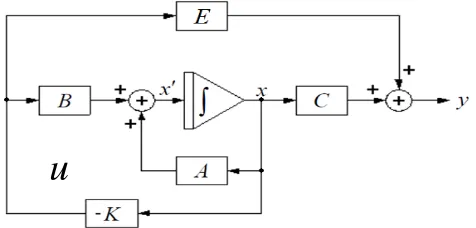
Where K is the feedback gain matrix This type of compensator is said to employ full-state feedback controller as presented in Fig -5.
Fig -5: Full-state feedback controller implementation
The closed-loop system in the state-space representation can be gathered by substituting Equation (26) into Equation (1) and (2):
(
A BK)
x x′= −(
C EK)
x y= −Stability depends on eigenvalues of A−BK. Thus to ensure the system is stable, the feedback gain matrix, K needs to be calculated. There are two methods that will be presented in this thesis to find the feedback gain matrix K; pole placement and optimal control technique.
4.1 FSFBC Based On Pole Placement Technique
As the name suggested, pole placement is a technique where poles are placed at desired location on the complex plane. For a full-state feedback controller, the matrix K (m x n) is used to place the poles of the system to desired location. The poles of the zeta converter are the eigenvalues of the state matrix A. The zeros of the system are unchanged although full-state feedback controller is used. The pole placement strategy is to improve the undesirable aspects of open-loop response such as overshoot, rising time, settling time and steady-state error. For this thesis, only the later aspect is considered for the compensator design.
Desired poles must be placed further to the left handside (on s-plane) of the system’s dominant poles location to improve the system steady-state error response. A good rule of thumb is that the desired poles are placed five to ten times further than the system’s dominant poles location [5].
For the full-state feedback controller, the closed-loop characteristic equation can be determined by:
(
−)
=0− A BK
I
λ
To determine the value of gain matrix K, the desired poles need to be placed. The number of desired poles depends on the system order. For a system that has an n-order, the poles are n, and the characteristic equation can be written as:
(
s−p1)(
s−p2)(
s−p3) (
Ls−pn)
=0Matrix K therefore can be determined by comparing the coefficients between characteristic equation in Equation (27) and (28).
4.2 FSFBC Based On Optimal Control Technique
Optimal control (also known as linear quadratic optimal control) is used to determine the feedback gain matrix, K other than pole placement. This method is different compared to pole placement technique since there is no need to determine where to place the desired poles. For optimal control, the (23)
(25)
u
(26)
(27)
__________________________________________________________________________________________
control input, u is determined such that the performance of the system is optimum with respect to some performance criterion. Basically, the goal is to design control elements that meet a wide variety of requirements in the best possible manner.
To optimally control the control effort within performance specifications, a compensator is sought to provide a control effort for input that minimizes a cost function:
(
)
∫
∞ + =0 x Qx u Rudt
J T T
Which is subjected to the constraint of the state equation.
Bu Ax x′= +
This is known as the linear quadratic regulator (LQR) problem. The weight matrix Q is an n x n positive semi-definite matrix (for a system with n states) that penalizes variation of the state from the desired state. The weight matrix R is an m x m positive definite matrix that penalizes control effort [3].
To solve the optimization problem over a finite time interval, the algebraic Ricatti equation is the most commonly used:
0
1 + =
−
+A P PBR−B P Q
PA T T
P B R K= −1 T
Where P is symmetric, positive definite matrix and K is the optimal gain matrix that is used in full-state feedback controller.
Since the weight matrices Q and R are both included in the summation term within the cost function, it is really the relative size of the weights within each quadratic form which are important. Holding one weight matrix constant while varying either the individual elements or a scalar multiplier of the other is an acceptable technique for iterative design. It is good to maintain an understanding of the effects of manipulating individual weights, however. In general, raising the effective penalty a single state or control input by manipulating its individual weight will tighten the control over the variation in that parameter, however it may do so at the expense of larger variation in the other states or inputs [6].
5. SIMULATION MODEL
Table -1 shows the parameters that are used for the zeta converter circuit. By substituting all the parameters in the state equations derived previously, the state matrices can be gathered as presented. Also, the eigenvalues for the zeta converter system can be calculated. Table -2 shows the pole placement group. Poles 3x, Poles 5x and Poles 7x refer to the
pole location at 3 times, 5 times and 7 times further than the most dominant eigenvalues that is at -7x10³ (real s-plane).
FSFBC gain, K for various pole location and cost function weight are calculated for the closed-loop compensation and are shown in Table -3 and Table -4, respectively. As for the Simulink model, the zeta converter open-loop and closed model with the implementation of full-state feedback controller is shown in Fig -6 to Fig -8.
Table -1: Zeta converter circuit parameters
− −
− −
− −
=
2 3
3 3
4 4
4
3 3
10 60 . 1 0
10 49 . 4 0
0 0
10 45 . 7 10 55 . 2
10 45 . 1 10 10 . 1 10 43 . 1 0
0 10
55 . 2 0
10 38 . 2
x x
x x
x x
x
x x
A
[
]
− =
3 3 4
3
10 49 . 4 0
0 0
10 08 . 5 10 2 . 1
0 10
45 . 7
x x x
x B
BS Z
[
1 1]
10 88 . 9 0 10 46 . 3
0 − −
= x x
C
[
]
[
1]
10 46 . 3 0 − −
= x
E ES Z
− =
0 10 36 . 3
10 75 . 4
10 50 . 3
4 5 5
x x x
Bd
(
)
32 ,
1 7.00 j9.91x10
p = − ±
(
)
34 ,
3 1.42 j1.09x10
p = − ±
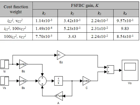
Table -3: FSFBC gain for various pole placement
Table -4: FSFBC gain for various cost function weight
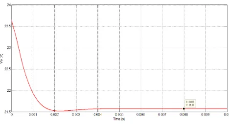
Fig -6: Open-loop zeta converter steady-state signal model
Fig -7: Open-loop zeta converter small-signal model
Fig -8: Closed-loop zeta converter model using full-state feedback controller
6. RESULTS
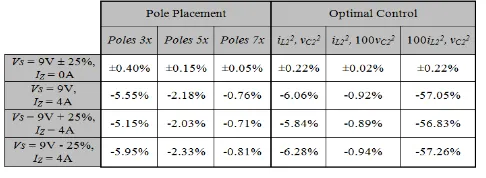
Table -5 shows the design requirement for the zeta converter. The desired output is 24V when the disturbances are within the allowable limit. Fig -9 to Fig -11 show the open-loop response for the zeta converter without any disturbance. For the open-loop, when subjected to input voltage disturbance of
ṽS=1V, the output increased significantly to approximately
27V (Fig -12). While for load current disturbance of ĩZ=1A,
the output decreased to about 21.6V (Fig -13). This response to disturbance is very undesirable.
Table -5: Zeta converter design requirement
To reduce the effect of the disturbances, full-state feedback controller is used. The controller is designed based on pole placement and optimal control technique. When subjected to
input disturbance of ṽS=1V, the response is shown in Fig -14.
In Fig -14(a), the pole location that yield the best compensation is Poles 7x with output voltage of 24.006V. while in Fig -14(b), cost function weight iL22, 100vC22 produced the best compensator with the output voltage of 24.002V. on the other hand, when subjected to load current
disturbance of ĩZ=1A, again Poles 7x (23.95V) and iL22,
100vC22 (23.95V) produced the best results as shown in Fig -16(a) and Fig -16(b), respectively.
Table -6 shows the summary of the voltage regulation when subjected to input voltage disturbance and/or load current disturbance for FSFSC based on pole placement and optimal
control technique. It is required that the VR is ≤ ± 1% (in
Table -5). For pole placement technique, only pole location at Poles 7x can achieve this requirement while for optimal control technique, iL22, 100vC22 can be used for the output voltage regulation requirement. Since both pole placement and optimal control technique can achieve required voltage regulation requirement, it is up to individual to choose their preference technique.
__________________________________________________________________________________________
Fig -10: Open-loop inductors current (iL1, iL2) responseFig -11: Open-loop capacitor voltage (vC1, vC2) response
Fig -12: Open-loop output voltage, VO response to
disturbance ṽS=1V
Fig -13: Open-loop output voltage, VO response to
disturbance ĩZ=1A
(a)
(b)
Fig -14: Compensated output voltage, VO response to
disturbance ṽS=1V using FSFBC based on:
(a) pole placement (b) optimal control technique
(a)
(b)
Fig -15: Compensated output voltage, VO response to
disturbance ĩZ=1A using FSFBC based on:
Table -6: Output voltage regulation using FSFBC based on pole placement and optimal control technique comparison
CONCLUSIONS
In this paper, modeling and control of a zeta converter operating in Continuous Conduction Mode (CCM) has been presented. The state-space averaging (SSA) technique was applied to find the steady-state equations and small-signal linear dynamic model of the converter. To ensure the output voltage maintain at the desired voltage regulation requirement, full-state observer and controller are used as the controller. To compensate the output voltage from the input voltage and load current disturbances, feedback controller gain for Poles 7x and (iL22, 100vC22) is proven to produce the best compensated output voltage for FSFBC based on pole placement and optimal control technique, respectively.
AFFILIATION
Department of Industrial Electronics, Faculty of Electronics and Computer Engineering (FKEKK), Universiti Teknikal Malaysia Melaka (UTeM), Hang Tuah Jaya, 76100 Melaka, Malaysia
ACKNOWLEDGEMENTS
The author would like to express gratitude to the Ministry of Higher Education (MoHE) Malaysia and Universiti Teknikal Malaysia Melaka (UTeM), Malaysia for the financial support.
REFERENCES
[1] E.Vuthchhay and C.Bunlaksananusorn, “Dynamic
Modeling of a Zeta Converter with State-space
Averaging Technique”, Proceedings of ECTI-CON
2008, pp. 969-972, 2008
[2] D.W.Hart, “Introduction to Power Electronics”,
Prentice-Hall Inc., 1997
[3] E.Vuthchhay and C.Bunlaksananusorn, “Modeling and
Control of a Zeta Converter”,The 2010 International
Power Electronics Conference, pp. 612-619, 2010
[4] E.Vuthchhay, C.Bunlaksananusorn and H.Hirata,
“Dynamic Modeling and Control of a Zeta Converter”,
2008 International Symposium on Communications and
Information Technologies (ISCIT 2008), pp. 498-503, 2008
[5] Charles L.Philips and H. Troy Nagle; “Digital Control
System Analysis and Design”, 1st Edition, Prentice-Hall Inc., 1984
[6] R.Tymerski and F.Rytkonen, “Control System Design”,
www.ece.pdx.edu/~tymerski/ece451/Tymerski_Rytkonen
.pdf, 2012
[7] M.Dahari and N.Saad, “Digital Control Systems –
Lecture Notes”,2002
[8] R. W. Erickson and D. Maksimovic, “Fundamentals of
Power Electronics”, 2nd Edition., Kluwer Academic Publishers,2001
[9] Ned Mohan, “Power Electronics and Drives”,
MNPERE, 2003
[10] Muhammad H. Rashid. “Power Electronics
Handbook”, Academic Press, 2001
[11] K.Ogata, “Modern Control Engineering”, 3rd Edition,
Prentice-Hall Inc., 1997
BIOGRAPHIES
Hafez Sarkawi received his BEng. Electrical
(Electronics) from Universiti Teknologi
Malaysia (UTM) in 2007 and MEng (Industrial Electronics and Control) from Universiti Malaya (UM) in 2012
Mohd Hafiz Jali received his BEng.
Electrical (Microelectronics) from Universiti Teknologi Mara (UiTM) in 2007 and MEng (Industrial Electronics and Control) from Universiti Malaya (UM) in 2012
Tarmizi Ahmad Izzuddin received his
BSc.&Eng. (Electronic Control System Eng.) from University of Shimane University, Japan in 2010 and MEng (Industrial Electronics and Control) from Universiti Malaya (UM) in 2012
![Fig -4: iL1 (left) and iL2 (right) waveform in CCM [3]](https://thumb-ap.123doks.com/thumbv2/123dok/549567.64532/3.595.317.551.114.188/fig-il-left-il-right-waveform-ccm.webp)