1
Design of a Low Voltage Class AB Variable Gain
Amplifier (VGA)
M.Idzdihar Idris, M.N.Shah Zainudin, M.Muzafar Ismail, R. Abd. Rahim
Universiti Teknikal Malaysia MelakaFaculty of Electronic and Computer Engineering, UTeM, Hang Tuah Jaya, 76100 Durian Tunggal, Melaka.
Abstract— Avariable gain amplifier (VGA) is one of the most significant component in many applications such as analog to digital converter (ADC). In communication receiver, VGA is typically employed in a feedback loop to realize an automatic gain control (AGC), to provide constant signal power to baseband analog-to-digital converter (ADC) for unpredictable received signal strengths. Gain range, power consumption and bandwidth of ADC are strongly influenced by the performance of operational amplifier. VGA is the key element for amplifying process in ADC. However, current class AB VGA is experiencing the limit of bandwidth, which is not suitable for high speed automatic gain control AGC. In order to overcome these limitations a high linearity and wide bandwidth of VGA is indispensable. The aim of this research is to get higher gain and larger bandwidth for VGA. In this research, a low cost, low power voltage and wide bandwidth class AB VGA is designed to mitigate this constraint. Superiority of the proposed VGA has been confirmed by circuit simulation using CEDEC 0.18-μm CMOS process with the help of tools from Mentor Graphics in designing a 100-MHz VGA under 1V supply voltage draining total static power consumption less than 125uW. The results show that the circuit is able to work with high linearity and wide bandwidth by varying Rf and Rs. Therefore, the frequency
response (Gain) and the wide bandwidth of this class AB VGA is better than previously reported class AB VGA. Consequently, this modified class AB VGA is appropriate for high speed applications.
Index Terms—VGA, ADC, CEDEC, CMOS
I. INTRODUCTION
GA is one of the most essential building blocks for low voltage applications such as wireless communication and mobile imaging applications low voltage applications such as wireless communication and mobile imaging applications [1-3]. Variable gain amplifier (VGA) is signal-conditioning amplifiers with electronically settable voltage gain. There are analog VGAs and digital VGAs, or DVGAs. An analog voltage controls the gain in both, which differ in how it is applied. VGAs are available from dc to gigahertz frequencies and in a variety of I/O configurations. Variable gain amplifiers (VGAs) have been used in a variety of remote sensing and communications equipment for more than a half-century. Applications ranging from ultrasound, radar, lidar to wireless communications and even speech analysis have
utilized variable gain in an attempt to enhance dynamic performance. In communication, receiver, VGA is typically employed in a feedback loop to realize an automatic gain control (AGC), to provide constant signal power to baseband analog-to-digital converter (ADC) for unpredictable received signal strengths. At present, a key design aspect for VGA is the low power dissipation, wide bandwidth and low cost [4]. Indeed, class AB has become very significant alternative for any application requiring VGA over the last few years [5-6].
VGA, as well as other circuits, are required to operate with low power supply voltage and low power consumption. As the process technologies develop, the maximum allowable supply voltage will scale down. It is inevitable that most low power integrated circuits will have to operate with power supply voltages between 1 V to 1.5 V. It is very challenging to design a VGA with high linearity and wide bandwidth with low supply voltage and low power consumption. Inaddition, VGA is generally required to maintain high linearity and low noise over the entire bandwidth and gain range. It is also important that the bandwidth of the amplifier remains constant when the voltage gain is varied and this can be obtained by employing current-mode techniques [7].
At present, current mode-technique has been extensively implemented in designing a VGA. A circuit using the current-mode technique has many advantages, such as, larger dynamic range, higher bandwidth, greater linearity, simpler circuitry and lower power consumption. In class-AB operation, each device operates the same way as in class B over half the waveform, but also conducts a small amount on the other half. As a result, the region where both devices simultaneously are nearly off is reduced. The result is that when the waveforms from the two devices are combined, the crossover is greatly minimized or eliminated altogether. The exact choice of quiescent current, the standing current through both devices when there is no signal, makes a large difference to the level of distortion and to the risk of thermal runaway that may damage the devices. Often the bias voltage applied to set this quiescent current has to be adjusted with the temperature of the output transistors [8].
2
operates in class-AB manner outperforms its predecessor(class-A), especially, in terms of signal swing and linearity while maintaining the same static power consumption and silicon area [11]. So in VGA, class AB amplifier is widely used.
A number of class AB VGA have been designed so far to achieve high linearity and wide bandwidth with acceptable power dissipation. However, researchers experienced gain limitation issues in wide bandwidth and the transistor’s size as well. P. Khumsat et. al implemented a low cost, low power and highly reliable class AB VGA in Spectre 0.18μm CMOS process [10]. The research showed that in designing a 50MHz VGA under 1V power supply, the highest frequency response (gain) is 25dB. However, it suffers from instability at high frequencies as mentioned before.
In this research, a low voltage class AB VGA for ADC is designed to attain the VGA with high dynamic range, high linearity and wide bandwidth with low power supply and low power consumption. This design overcomes the limitations of the conventional class AB VGA. Current mode technique has been used in this design to achieve better circuit performance. Small size of transistor is used in this design to reduce the size of circuit and cost as well. The proposed class AB VGA amplifier is designed in CEDEC 0.18μm process. Simulations results show that the modified low voltage class AB VGA performs better than the sense amplifier designed by P. Khumsat et. al.
II. CLASS ABOUTPUT STAGES
The amplifier output stage is an important part of an operational amplifier, as it is the stage that delivers the input signal to the load. In a well-designed two or three-stage operational amplifier it is also the stage which consumes most of the amplifier biasing current and ultimately sets limits on linearity of the amplifier and its maximum tolerated capacitive load. When the operating environment of an amplifier requires it to drive low ohmic resistive loads, high current source loads or large capacitive loads, the output stage must be able to source and sink currents that greatly exceed its biasing current. In practise this requires some kind of common drain-based class AB output stage, as shown conceptually in Fig. 1, at least in a low voltage environment, in order not to degrade the available dynamic range any further.
Fig. 1. A conceptual common drain stage-based class AB output stage.
III. TWO STAGE CURRENT MODE VARIABLE GAIN AMPLIFIER The previously proposed VGA in [10] has shown its versatility and potential to operate at low supply voltage, low power consumption with high bandwidth while maintaining good degree of dynamic range and occupying small silicon area. This VGA’s architecture is presented in Fig. 2, which is a cascade of a linear transconductance cascaded and a linear transimpedance amplifier with shunt-feedback resistors (Rf).
Fig. 2: Architecture of the proposed VGA stage in [10].
This allows constant bandwidth when varying the voltage gain. The voltage gain of the VGA circuit is the product of the transconductance gain (Gm) and the transimpedance gain (Rm).
The transimpedance gain is given by
(1) where Rin and Ai, respectively, are the input resistance and the
current gain of the current amplifier. Note that, when Ai >> 1, we have Rm≈ –Rf. There, a linear Gm and a high-gain current
3
proposed VGA circuit realization in CMOS is also depicted inFig. 3. The circuit is very compact; however it has a bandwidth limitation at which the bandwidth is restricted to 50MHz and using the big size of transistor. Table 1 shows parameter or size of transistor that have been used in previous circuit.
Fig. 3: Circuit realization of the proposed circuit [10] with CMOS
Table 1: Previous circuit’s [10] transistor size of VGA operating under a 1 V supply power.
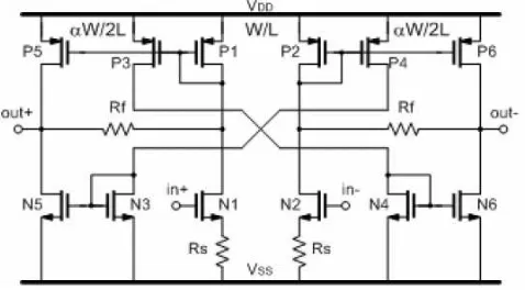
Fig. 4 shows the circuit implementation of the proposed VGA cell, which combines a source degeneration differential input transconductance amplifier (N1 – N2, Rs) and a
current-mode transimpedance amplifier (P1 – P6, N3 – N6) in order to maximum transconductance/bias current efficiency and minimize supply voltage and noise [13-14] . Cascaded current mirrors are used to implement the DC current sources. Despite these advantages, such structure possesses a serious drawback in being unable to reject common-mode signal. The second stage mirror-based current amplifier (P1 – P6, N3 – N6) resolves this problem by employing feed forward technique that allows differential signals to be constructively combined while on the other hand cancel a common-mode signal [15-16]. This current amplifier combined with feedback resistors Rs form a transimpedance amplifier necessary for current-to voltage conversion. Moreover, such output stage also provides a class-AB operation allowing larger signal swing compared to its predecessor presented in [17-18]. Thus the major advantage of such VGA circuit is its ability to offer excellent signal linearity without sacrificing the original advantages on both aspects of the power consumption and circuit complexity.
(We are unable to place the figure here due to its size which is placed at the
below of the manuscript)
Fig. 4: Improved VGA based on the structure in Fig. 1a with class-AB output stage and signal feed forward topology.
It is important to note that the size of each transistor is reduced according to the ratio (W/L) to get a smaller size of IC. Besides that, the number of resistor Rs that have been used in previous circuit is also reduce from 2 to 1.Table 2 shows the comparison size of transistor between this work and previous circuit.
Table 2: Comparison of VGA transistors
Transistor
A small-signal transconductance of the first stage is simply expressed as
(2) where gm and Cgs are respectively transconductance and gate
source capacitance of N1 and N2. The amplifier differential current gain Ai and input resistance Rin have been analyzed to
be
equivalent total capacitance (referred to ground) at gates of P1 (P2) and N3 (N4) whose values are mainly contributed from gate-source capacitance. At low frequency, since gmx =
gmi(α/2), thus Ai of Fig. 4 equals to α, which is the same as
4
substituting (3) and (4) into (1), a small-signal transimpedancegain could be obtained to be
(5)
The feedback resistor Rf is selected to set a voltage gain range
whereas a source degeneration resistor Rs is tuned to vary the
amplifier gain. The minimum value of Rs sets the maximum gain for a specific gain range (as previously set by Rf) and it
also defines the maximum static current consumed by the VGA. The similar technique proposed in [19] can be used to tune the grounded resistor Rs.
V. RESULT AND DISCUSSION
The improved class AB VGA circuit with a single 1V power supply voltage have been designed and simulated in CEDEC 0.18-μm CMOS process. Simulations were executed to evaluate the circuit performance of the modified class AB VGA with the previously reported class AB VGA [10].With α = 5, transistor sizing of the VGA circuit is listed in Table 3. The minimum value of Rs is chosen to be 500 Ohms to ensure
a maximum power consumption not exceeding 120uW for a bandwidth over 100MHz.
Table 3: Transistor sizing within the VGA operating under a 1V supply voltage.
By using a transient analysis within Mentor Graphics design architect IC (DA-IC), Fig. 5 depicts the input and output signal swing at the maximum voltage gain of 26dB where we can see that the output signal is amplified.
(We are unable to place the figure here due to its size which is placed at the
below of the manuscript)
Fig. 5: Simulation result of output swing at maximum voltage gain of 26 dB for 1V power supply.
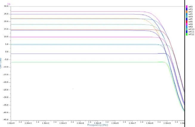
Fig. 6 shows four families of curves of measured gain response, which was obtained by setting the feedback resistors (Rf) from 15k to 500k. This renders coarse gain tuning of the
amplifier, where high gain settings (upper family of curves) and low gain settings (lower family of curves) can be achieved with Rf = 500k, and Rf = 15k, respectively. Within each family
of curve, the value of Rs was changed to obtain fine gain
tuning. It can be seen that voltage gain control with constant bandwidth can be achieved by varying Rs, while changing Rf
affects the bandwidth of the VGA because Rf determines the
dominant output pole frequency of the circuit. Therefore to design the VGA, Rf should be chosen first according to the
bandwidth requirement and Rs is then tuned to adjust the voltage gain.
(We are unable to place the figure here due to its size which is placed at the
below of the manuscript)
Fig. 6: Frequency response of the VGA where Rf: 500kΩ, 150kΩ , 50kΩ, 15k
Ω and Rs: 500Ω, 5kΩ, 15kΩ.
A comparisons study of class AB VGA between this work and P. Khumsat et. al is shown in Table 4. From the study, it is shown that the circuit is able to vary the voltage gain in linear dB manner from -7 to 26 dB. The total power consumption is less than 125uW from a single 1 V power supply voltage and has a wide and constant bandwidth, which is better than the P. Khumsat et. al. Table 4 also summarizes the experimental performance of the overall class AB VGA. It can see that the proposed class AB VGA can achieved the similar gain range to other reported VGA, while operating under lower supply voltage and smaller size transistor indicating that the proposed VGA is more superior.
Table 4: VGA performance comparison
Parameters This work Circuit in [10]
Technology CEDEC 0.18um
CMOS Spectre 0.18um CMOS
Bandwidth ~100Mhz ~50Mhz
Gain range at constant
bandwidth 26dB 25dB
5
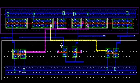
Fig. 7: A layout design of class AB variable gain amplifierVI. CONCLUSION
An improved design and a comparative study of class-AB variable gain amplifier using two stage architecture comprising a linear transconductor cascaded by a current amplifier-based feedback transimpedence amplifier is presented in this research. The modified circuit has been designed by using the CEDEC 0.18-μm CMOS. In this research, small design parameters were used to reduce the cost and die size of whole chip. According to the research results, it has been proven that, the circuit is capable to achieve high linearity and wide bandwidth. The results also verify that by using current mode technique, the voltage gain of the VGA can be tuned while the bandwidth remains constant. Additionally, the circuit size reduced significantly by using small transistors and less number of resistor.
REFERENCES
[1] W. A. Serdijn, A. C. Van der Woerd, J. Davidse, and A. H. M. Van, Roermund, “A low-voltage low-power fully integratable automatic gain control for hearing instruments,” IEEE J. Solid-State Circuits, Vol. 29, pp.943-946, Aug 1994.
[2] R. Harijani, “A low-power CMOS VGA for 50 Mb/s Disk Drive Read Channels,” IEEE Trans. on Circuits and Systems-II: Analog and Digital Signal Processing, Vol. 42, no. 6, pp. 370-376, June 1995.
[3] G. S. Sahota and C.J Persico, “High Dynamic Range Variable Gain Amplifier for CDMA Wireless Application,” in Proc. 1997 IEEE International Solid-State Circuits Conference, pp. 374-375, 1997. [4] Hee-Cheol Choi, Young-Ju Kim, Myung-Hwan Lee, Young-Lok Kim,
and Seung-Hoon Lee, “A 12b 50MS/s 10.2mA 0.18μm CMOS Nyquist ADC with a Fully Differential Class-AB Switched OP-AMP”, IEEE Journal of Solid-State Circuits, Vol. 45,No 3, March 2010.
[5] Fan You, S. H. K. Embabi, and Edgar S´anchez-Sinencio, “Low-Voltage Class Buffers with Quiescent Current Control”, IEEE JOURNAL OF SOLID-STATE CIRCUITS, VOL. 33, NO. 6, JUNE 1998.
[6] Vincenzo Peluso, Peter Vancorenland, Augusto M. Marques, Michel S. J. Steyaert, Willy Sansen, “A 900-mV Low Power ∆∑ A/D Converter with 77-dB Dynamic Range”, IEEE JOURNAL OF SOLID-STATE CIRCUITS, VOL. 33, NO. 12, DECEMBER 1998.
[7] K. Phang, D. A. Johns, “A 1 V 1 mW CMOS Front-End with On-chip Dynamic Gate Biasing for a 75Mb/s Optical Receiver,” IEEE Int. Solid-Stage Circuits Conference, pp. 218-220, 2001.
[8] Chuanzhao Yu, J. S. Yuan, “Electrical and Temperature Stress Effects on Class-AB Power Amplifier Performances”, IEEE TRANSACTIONS ON ELECTRON DEVICES, VOL. 54, NO. 6, JUNE 2007.
[9] Antonio J. López-Martín, Sushmita Baswa, Jaime Ramirez-Angulo, Ramón González Carvajal, “Low-Voltage Super Class AB CMOS OTA Cells With Very High Slew Rate and Power Efficiency”, IEEE JOURNAL OF SOLID-STATE CIRCUITS, VOL. 40, NO. 5, MAY 2005. [10] P. Khumsat, A. Thanachayanont, S. Sakphrom, “A Compact Class-AB CMOS Variable Gain Amplifier”, ECTI International Conference, pp. 85-88, 2007.
[11] Hervé Facpong Achigui, Christian Jésus B. Fayomi, Mohamad Sawan, “1-V DTMOS-Based Class-AB Operational Amplifier: Implementation and Experimental Result”, IEEE JOURNAL OF SOLID-STATE CIRCUITS, VOL. 41, NO. 11, NOVEMBER 2006.
[12] Yan Wang, Pavan Kumar Hanumolu, Gábor C. Temes, “Design
Technique for Wideband Discrete-Time Delta-Sigma ADCs With Extra Loop Delay”, IEEE TRANSACTIONS ON CIRCUITS AND SYSTEMS— I: REGULAR PAPERS, VOL. 58, NO. 7, JULY 2011.
[13] Gerry Taylor and Ian Galton, “A Mostly-Digital Variable-Rate Continuous-Time Delta-Sigma Modulator ADC”, IEEE JOURNAL OF SOLID-STATE CIRCUITS, VOL. 45, NO. 12, DECEMBER 2010. [14] Omid Rajaee, Tawfiq Musah, Nima, Maghari, Seiji Takeuchi, Mitsuru
Aniya, Koichi Hamashita, Un-Ku Moon, “Design of a 79 dB 80Mhz 8X-OSR Hybrid Delta-Sigma/Pipelined ADC”, IEEE JOURNAL OF SOLID-STATE CIRCUITS, VOL. 45, NO. 4, APRIL 2010.
[15] S. Rabii and B. A. Wooley, “A 1.8-V Digital-Audio Sigma-Delta Modulator in 0.8-_m CMOS,” IEEE Journal of Solid-State Circuits, vol. 32, pp. 783-796 , June 1997.
[16] P. Khumsat and A. Worapishet, “Compact Two-Stage Class-AB CMOS OTA for Low-Voltage Filtering Applications,” IEICE Transactions on Electronics, Vol. E90-C, No. 2, pp. 543-546, February 2007.
[17] A. Thanachayanont and P. Naktongkul, “Low-voltage wideband compact CMOS variable gain amplifier,” Electronics Letters, vol. 41 No. 2, January 2005.
[18] P. Naktongkul and A. Thanachayanont, “1.5-V 900uW 40-dB CMOS variable gain amplifier,” Proceedings of 2006 IEEE International Symposium on Circuits and Systems, May 2006.
![Fig. 2: Architecture of the proposed VGA stage in [10].](https://thumb-ap.123doks.com/thumbv2/123dok/561483.66268/2.612.383.496.61.193/fig-architecture-proposed-vga-stage.webp)