A Simple Energy Recovery Scheme to Harvest
the Energy from Shaded Photovoltaic
Modules During Partial Shading
Mohd. Zulkifli Ramli and Zainal Salam
, Member, IEEE
Abstract—This paper proposes a simple circuit to recover the energy that otherwise would be lost due to the partial shadings on photovoltaic (PV) modules. Since the circuit can be readily retrofitted to an existing PV system, no modification on the central inverter is required. The main idea of the scheme is that, during partial shading, parts of the current from the nonshaded modules are harvested by an energy recovery circuit using power electronic switches and storage components. In doing so, the current of the PV string is maintained at the level generated by the shaded mod-ule. There is no need for the shaded module to be short-circuited; as a result, it can still actively produce output power (despite being partially shaded). To investigate the idea, the proposed circuit is retrofitted to a prototype PV system using eight modules. The par-tial shading conditions are emulated using a solar simulator with a controllable irradiance capability. The results are validated by a good agreement between the experimental and simulation works.
Index Terms—Energy recovery, inverter, maximum power point (MPP), maximum power point tracking (MPPT), partial shading, photovoltaic (PV).
I. INTRODUCTION
F
OR many years, the central inverter has been the prefer-able choice for large as well as small photovoltaic (PV) system installations [1], [2]. In this configuration, a number of PV modules are connected in series to form a string. Sev-eral of these strings are arranged in parallel to form an array, which is then connected to one central inverter. This is known as series-parallel connection and is a typical setup for the PV power generation system. The merits of the PV system with central inverters are well known: simple installation, less main-tenance, and high reliability [3], [4]. However, it does exhibit several disadvantages, one of which is the severe reduction in the throughput power when one or a number of modules are sub-jected to partial shading [1], [5]–[11]. In the building integratedManuscript received April 25, 2013; revised September 2, 2013 and Decem-ber 1, 2013; accepted January 7, 2014. Date of publication January 24, 2014; date of current version August 13, 2014. This research was supported by the Ministry of Higher Education Malaysia, under the Research University Grant 2423.00 G40. The project is managed by the Research Management Centre, Uni-versiti Teknologi Malaysia. Recommended for publication by Associate Editor V. Agarwal.
M. Z. Ramli is with the Faculty of Electrical Engineering, Universiti Teknikal Melaka,76100 Melaka, Malaysia (e-mail: [email protected]).
Z. Salam is with the Centre for Electrical Energy Systems, Faculty of Electri-cal Engineering, Universiti Teknologi Malaysia, 81310 Johor Bahru, Malaysia. (e-mail: [email protected]).
Color versions of one or more of the figures in this paper are available online at http://ieeexplore.ieee.org.
Digital Object Identifier 10.1109/TPEL.2014.2302007
PV system, the shading normally originates from the nearby tree, building, chimney, power line poles, or similar objects. These factors may be unavoidable due to the building congestion in urban areas and unforeseen erection of new structures. In a large PV power generation system (PV farm), the partial shading can be caused by clouds that strike on certain spots of the solar array, while other parts are left uniformly irradiated. In certain cases, the remains of birds or animals cause the shading on the modules. Another source of partial shading-like characteristics is exhibited by module irregularities; a common example would be the presence of cracks on one or more modules of the PV array.
With the presence of partial shading, the behavior of the PV system becomes very complicated. This is because the shaded module acts as a load instead of a generator; consequently, a hot spot is created and if left unprotected, the module may experi-ence irreparable damage. Typically, every module is connected to a bypass diode to divert the current in the case of partial shad-ing occurrence. However, when the bypass diode is activated, theP–Vcharacteristic curve exhibits multiple peaks, i.e. several local along with one global peak [5], [6], [12]–[15]. If the system is equipped with the conventional maximum power point track-ing (MPPT) such as perturbed and observed (P&O), increment conductance or Hill-climbing, it would be very difficult to track the true maximum power point (MPP) peak because these algo-rithms could not discriminate between the local and the global peaks. In most cases, the MPPT will settle at a local peak, possibly resulting in a huge loss of power [1], [6], [16]–[18]. Furthermore, when the current flows through the bypass diode, conduction losses occur, further degrading the system’s efficiency.
There are efforts using sophisticated MPPT schemes such as modified P&O [6], [19]–[22], particle swarm optimization [13], [20], [23], ant colony optimization [24] and the direct search method [25]. Despite the success of these algorithms to track the global peak [13], [23], [26], it must be noted that as long as the shaded module is being short-circuited by the bypass diode, it is totally unusable. However, the shading phenomena may not always be so severe such that the module receives zero irradiance. It is known that, depending on the severity of the shading, there is a certain amount of power that could possibly be captured by the shaded module. Despite this fact, the opportunity to harvest this power is lost due to the activation of the bypass diode.
Hence, various methods are devised to recover the power from the shaded module. One approach is to place a small
dedicated dc–dc converter to every module; then these mod-ules are connected to the central inverter [5], [12], [26]–[28]. In the literature, this method is known as the distributed MPP configuration. The converter normally has a power rating ap-proximately equal to the module itself and is equipped with its own MPPT controller. Using this scheme, the nonshaded mod-ules are not affected by the shaded ones, and the power from the latter can be independently harvested. Although attractive, the method inhibits several shortcomings. During normal op-eration, the converter conducts the full load current, resulting in high conduction and switching losses [28]. Furthermore, the reliability of the electronic components is reduced due to their exposure to harsh environment conditions, particularly high op-erating temperature. This is unavoidable since the converter is mounted underneath the module itself [29], [30]. Alternatively, there are considerable efforts to develop the dc–ac converter for each module (known as microinverter), which is directly con-nected to the ac grid [3], [26], [27], [31]–[37]. Using the concept, the central inverter is not required because the microinverter has its own MPPT and inversion and voltage step-up mechanism.
Another method to utilize the power from the shaded modules is proposed by the authors in [38]. In this technique, a bidirec-tional buck–boost, flyback or Cuk converter is used to divert the current of the nonshaded modules by controlling the duty cycle of the converters. During partial shading, the energy from the nonshaded modules is transferred to the inverter and con-sumed by the PV system. The work in [30] only demonstrates the workability of the approach using two modules per con-verter. However, to accommodate more than two modules, the converters need to be overlapped to allow for the string current from the nonshaded module to be properly diverted. As a re-sult, for every interconnection between a group of two modules, additional two switches and two diodes are required. A similar scheme, albeit using a different circuitry, has been proposed by Shimizuet al[14]. Despite its effectiveness, the main drawback of the scheme is the switching limitation; for example, for four modules in series, the off duty cycle range is limited to 25%. For higher number of modules, the off duty cycle is even lower. This is because within a single switching cycle, only one switch is forced to be turned OFF, while others remain ON. The lim-ited off duty cycle restricts the ability of the circuit to control the power flow under severe shading condition. In addition, al-though the scheme utilizes MPPT to improve the efficiency of the circuit, the authors do not mention its performance during partial shading and how it is synchronized to the MPPT of the central inverter. There are also concerns regarding the accuracy of the voltage and current sensors (used for MPPT computation) when subjected to the high temperature beneath the modules.
In [39], an alternative method using a single inductor per four modules is proposed. Despite the reduced inductor, the cir-cuit requires a large number of switches and diodes, i.e. for a four-module system, eight switches and ten diodes are needed. Furthermore, during the inductor charge and discharge cycles, only one combination of switches and diodes is switched ON and OFF; others are not active. Under this constraint, the best switching combinations have to be found in order to deliver the maximum power during partial shading. However, in many
cases, the search for the optimum switching configuration is complex and requires a substantial amount of time. Thus there are possibilities that the algorithm may not be able to cope with rapidly changing cloud condition. For example, as described in [25], the fluctuation in irradiation can go up to 15 times within 1 minute. If the partial shading occurred during this period, an efficient tracking could not be guaranteed. More recently, an energy recovery scheme for shaded module for the multilevel inverter is reported [40]. Despite its ability to harvest the power during partial shading, the buck converter always conducts at full load current during a normal condition. This causes high switch-ing and conduction losses. Another drawback of this technique is the complexity of the switching due to the multilevel inverter structure.
With regard to these issues, this paper describes an attempt to improve the capabilities of the topologies described above. The proposed scheme is based on a group of four modules (one unit), but can be extended to accommodate a large number of modules by combining other units using a simple interconnecting circuits. The number of switches for four modules (one unit) is 1, and for the interconnection of two units, an additional two switches and one inductor are needed. The circuit is only active during the event of partial shading; during uniform irradiance, it is isolated from the PV system. Besides, the switching pattern for the switch is simple, i.e. it operates based on an opened-loop concept, using a fixed 50% duty cycle. Consequently, the scheme can be implemented using a low cost digital circuit, which is much simpler than the closed-loop system proposed by the authors of [12] and [30]. The latter requires microcontrollers, current, and voltage sensors for MPPT computation. In average, the circuit utilizes 0.5 inductor per module, compared to one per module for topologies in [12], [14], and [38]. Since the circuit is readily retrofitted to the PV system, no modification into the existing central inverter is required. It can be plugged under the module with minimal additional wirings.
It has to be noted that the idea and concept of this topology was initially published in [8]. However, in that paper, there is in-sufficient detail on the analysis of the circuit operation. Further-more, limited results are presented, i.e. the circuit performance is illustrated by only four modules, which implies that the inter-connection circuit between the different units is untested. In this paper, an extensive analysis is carried out to describe the oper-ation of the energy recovery circuit from shaded modules. An experimental test rig involving eight (retrofitted) PV modules, along with an in-house solar simulator, is constructed. Using the solar simulator, various partial shading conditions are emulated to verify the performance of the proposed circuit. The efficiency of the proposed work is evaluated against the typical PV sys-tem (i.e. with the bypass diode only). It is envisaged that the improvements mentioned previously yield a satisfactory return of investment over the long run.
II. PROPOSEDCIRCUIT
A. General Block Diagram
Fig. 1 Overall block diagram of the proposed PV power generation system retrofitted to a grid-connected PV.
Fig. 2 Trigger circuit.
is connected in parallel to the original PV modules; therefore, it can be easily retrofitted to the existing system with minimum changes in the electrical wirings. In Fig. 1, the PV system is a grid-connected type using one central inverter with MPPT. However, the proposed circuit can be equally effective for stan-dalone system, for example, using battery banks. Note that the circuit only functions during the occurrence of partial shading. Under the uniform irradiance, the PV system operates in the normal way, i.e. the bypass diode is in the OFF state. During this condition, the circuit draws minimal power, just enough to maintain the operation of the trigger circuit.
When partial shading occurs, the trigger circuit is automati-cally turned ON and it activates the energy recovery circuit— thus bypassing the bypass diode. From then on, the energy re-covery circuit will start the process of recovering the power from the shaded module, which shall be detailed in the following sec-tion. For brevity, in Fig. 1, only two PV modules are shown. However, the system can be expanded to 4, 8, 16, 32 modules, and so on using a simple interconnection scheme.
B. Trigger Circuit
The details of the trigger circuit are shown in Fig. 2. During the normal operation (i.e. uniform irradiance), the proposed cir-cuit is cut-off from the modules. Thus the PV system operates as if the proposed circuit does not exist. However, if partial shading occurs on PV1, for example, its associated bypass diode will be shorted-circuited. The differential amplifier will sense the low voltage (across the diode) and then compare it with a voltage trigger, Vt. If a certain condition is satisfied, the comparator
enables the gate signal and thus triggers the energy recovery circuit. Once the recovery circuit is activated, the voltage across PV1 rises. The bypass diode is now open-circuited, and PV1 is directly connected to the energy recovery circuit. Consequently,
Fig. 3. Basic unit energy recovery circuit.
the process of recovering the power from the shaded module (PV1) begins.
C. Energy Recovery Circuit
Once the partial shading condition is detected, the energy re-covery circuit is turned ON by enabling the gate drivers of the switches. To illustrate the recovery concept, a string of four PV modules is used as shown in Fig. 3. For simplicity, a constant current source is used to represent the output power (when mul-tiplied by the PV voltage) drawn from the PV system at MPP. This is acceptable since the objective of the work is to show the effectiveness of the circuit when dealing at the input side of the PV system. This approach is suggested in [41] to avoid com-plexities in the analysis as well as the simulation. In addition, since the bypass diode is not activated during partial shading, it can be removed to simplify the analysis.
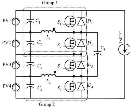
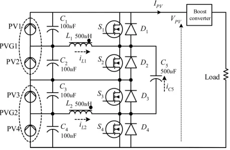
The basic unit of this topology comprises of four PV mod-ules, which is divided into two groups. Group 1 involves PV1 and PV2, together with their corresponding power elec-tronics circuit, comprising ofS1, D1, L1, C1, S2, D2, andC2. These components form what is referred to (in this paper) as the “within group” circuit. Group 2 includes PV3, PV4 with
S3, S4, D3, D4, L2, C3, andC4. In order to connect the groups (or “intergroup”), the capacitorC5 is used. One of the main advantages of the circuit is that the duty cycles of all switches are fixed at 50%. So, only simple control logic is used to control the switches.
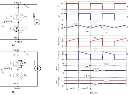
Fig. 4. Circuit operation within group when PV1 is shaded, while PV2 is not shaded: (a) Mode 1 and (b) Mode 2.
lesser amount, depending on the shading condition) because its voltage is not zero. Meanwhile, the energy stored inL1will be released back to the output viaD1 (by turning OFFS2). Thus, ideally, using this scheme, no PV power is wasted except for the losses due to the switches, diodes, and the nonidealities of the passive components. Note that a dead time of 400 ns is applied during transition of the paired switches, for example, between
S1 andS2. However, the dead time does not affect the overall behavior of the system.
III. OPERATIONALMODES ANDANALYSIS
A. Operation “Within-Group”
The operation of the circuit within the group can be divided into two modes, which are defined by the states of the switches in the circuits. During the MPP, both the PV and the load are reacting as a constant current source. Therefore, to simplify the analysis [39], at the MPP, the total current of both PV modules is replaced by a constant current source(IM PPT), as shown in Fig. 4. Furthermore, the nonidealities of the components are also omitted.
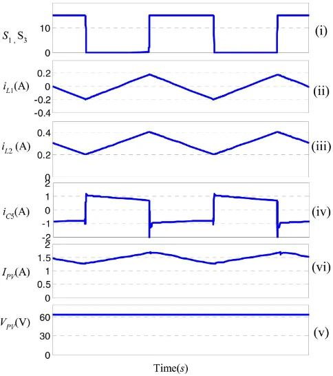
Mode 1 (t0 < t< t1):The operation of the circuit during Mode 1 is shown in Fig. 4(a). Its corresponding timing diagram is shown in Fig. 5. In this mode,S2 is turned ON, while S1 is turned OFF. The current flows throughS2, causing iL1 to increase linearly due to the constant voltage supply from PV2. Hence, part of the energy from the nonshaded module (PV2) is
Fig. 5. Timing diagram for group 1 of the proposed method.
temporarily stored inL1. This can be understood by observing the current waveforms in tracecof Fig. 5. The ripple current of
L1can be expressed as ∆IL1 =
VPV 2DT
L1 (1) where∆IL1 is the ripple of the inductor current, i.e.(Im ax−
Im in), whileD andT are the duty cycle and the period of the switching, respectively.
Mode 2(t1 > t > t2):In this mode,S1is turned ON andS2 is turned OFF, as shown in Fig. 4(b). WhenS2 is turned OFF, the current is forced to flow through the freewheeling diode,D1. This current is shown by the traceein the timing diagram. The stored energy inL1 is released in the form of current and flows to the load. Since the duty cycle of the circuit is fixed at 50%, the average inductor current,(iL1)is divided equally to formIW1 andIW2. Furthermore, the ac components ofIW1andIW2 are filtered by the capacitorsC1 andC2; thus, only the dc currents flow to the load. The load current,IPV (which is equal to the average PV string current) at Node 1 can be written as
IPV =IPV 1+IW1 (2) where IPV1 is the string current (note:IPV1 is limited by the PV1 current). However, at Node 2, the same current can be expressed as
Since the duty cycle is 50%, it follows that
IW2 =IW1 =
IW
2 . (4)
Therefore
2IPV =IPV 1+IPV 2
IPV =
IPV 1+IPV 2
2 . (5)
Equation (5) indicates that the total current to the load (at MPP) is contributed by the nonshaded module as well as the shaded one. In another word, the proposed circuit acts as a “bal-ancing” element to equalize the currents between the shaded and nonshaded modules such that the current at Node 1 equals Node 2. This implies that during the occurrence of partial shad-ing, the energy from the shaded module is recovered and trans-ferred to the load. Since the output current is increased, while the voltage across the shaded voltage is near itsVM P, the
over-all energy yield is increased. This is in contrast to the bypass diode method, in which the energy from the shaded module is not usable because the voltage across it is zero.
For further clarification of the concept, the numerical values of currents are used for simulation in Fig. 5. In this case, the PV1 and PV2 currents are 2 A and 4 A, respectively. The resulting average load current is 3 A, which is in accordance with (5).
B. Operation: “Intergroup”
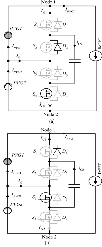
When more than two groups are connected in series (to form a unit), the intergroup connectivity is required. The intergroup operation can be explained using Fig. 6. For clarity, capacitors
C1, C2, C3, andC4 (which act as filters), and L1 andL2 are removed because they are not involved in the intergroup inter-action. Note that PGV1 is the series combination of PV1 and PV2 after the currents of the shaded and nonshaded modules are successfully balanced. Similarly, PGV2 is a series combination of PV3 and PV4. For the purpose of discussion, PVG1 is des-ignated to be the shaded group, while PVG2 is the nonshaded one.
Mode 1 (t0< t < t1): The intergroup operation during
Mode 1is shown in Fig. 6(a). Its corresponding timing diagram is shown in Fig. 7. In this mode,S2andS4 are simultaneously turned ON, whileS1andS3are turned OFF. The current flows throughD2andS4, causing the capacitorC5to be charged. Con-sequently, part of the energy from the nonshaded group (PVG2) is temporarily stored inC5.
Mode 2(t1 > t > t2):In this mode, the energy previously stored inC5 (duringMode 1) is released to the output. This is achieved by turning ONS3as shown in Fig. 6(b). Since the duty cycle of S3 is 50%, IG is divided equally to formIG1 and IG2. The MPPT current, IPVG at Node 1 can be written asIPVG =
IPVG1 +IG1. At Node 2, the same current can be expressed as IPVG =IPVG2−IG2.Using the similar analysis as in the
previous section, the average PVcurrent that flows to the output can be written as
IPVG =
IPVG 1+IPVG2
2 . (6)
Fig. 6. Circuit operation intergroup when group 1 is shaded, while group 2 is not shaded: (a) Mode 1 and (b) Mode 2.
From (6), it can be observed that the total MPPT current is the contribution by the nonshaded intergroup as well as the shaded one. Effectively, the circuit provides a path for higher current of the nonshaded group to flow so that the current from the shaded group can be utilized. It should be noted that if a bypass diode is used, the voltage across the shaded modules is zero; consequently, no power can be harvested from them.
Fig. 7. Timing diagram of intergroup operation of the proposed method.
Fig. 8. Proposed circuit with eight PV modules.
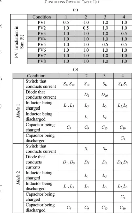
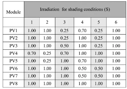
Table I(b) summarizes the states of all switches and diodes, as well as the charging and discharging of inductor and capacitors for eight modules. Different partial shading conditions are im-posed, as shown in Table I(a). To be consistent with the earlier analysis, the modules are intergrouped and labeled as follows: [PVG1 = PV1 + PV2], [PVG2 =PV3 + PV4], [PVG2 = PV5+PV6], and [PVG4=PV7+PV8]. In addition, the nes-tled intergroup is defined as: [PVBG1=PVG1+PVG2] and [PVBG2=PVG3+PVG4]. At the output side of the circuit,
TABLE I
(a) SHADINGCONDITIONS FOREIGHTMODULES. (b) STATES OFSWITCHES, INDUCTORS,ANDCAPACITORSWHENSUBJECTED TOSHADING
CONDITIONSGIVEN INTABLEI(a)
the boost converter (with P&O MPPT), the PI controller, and the load are interconnected to emulate theIM PPT (as shown in Fig. 6).
As an example, for shading Condition 1, only PV1 is shaded. It receives 0.5 S (1.0 S=1.0 kW/m2) while the rest of the mod-ules are fully irradiated (at 1.0 S). DuringMode 1,S2 conducts the current and starts to chargeL1. InMode 2,D1 is conduct-ing, and the energy is discharged from L1. In order to allow for higher current from PVG2 to flow to the output, it needs a new current path, which is provided byC9. In this situation,
D9 inMode 2. The operation for Conditions 2 and 3 are simi-lar as above, but the modules are subjected to different shading patterns. For Condition 4, the total of irradiation of PVBG1 and PVBG2 is equal, but the shading locations are interchanged. There is no need to provide a current path between PVBG1 and PVBG2; bothS9 andS10 can be turned OFF. However in this work,S9 andS10 are turned ON and OFF alternately, in synchronization withS1andS2.
IV. EXPERIMENTALSETUP
A. Simulation Model
The proposed energy recovery system is validated using MATLAB-Simulink simulation as well as experimental pro-totype. Two sets of experiments are carried out. The first set utilizes four PV modules, i.e. one unit. The purpose is to verify the analysis given in Section III. The second experiment is us-ing eight (two units) modules, as shown in Fig. 8. For the PV simulation, the two-diode model of the solar cell is used [42] as it gives more accurate results than the more popular single diode model. For consistency, the same circuit is used for hard-ware verification. Experimentally, the BP-MSX60 PV module is used. Its peak rated power is 60 W (3.5 A/17.1 V) at stan-dard test conditions (STC). The original manufactured module is modified (by rearranging its internal wiring) such that it be-comes two modules (8.55 V, 30 W each). Thus the totally rated power for the experimental rig at STC is 240 W.
B. Power Circuit
The power circuit is constructed using ten IRFB4332 PBF MOSFETs. This device has an integrated freewheeling diode; thus no (additional) external diode is required. The values of inductors(L1−L4)are 500µH. These are computed by con-sidering the allowable inductor current ripple, based on (1). The capacitors(C1−C4)are chosen to be 100µF; the values are derived by simulation. The PV (along with the proposed circuit) is connected to a boost converter. The latter is equipped with the P&O MPPT algorithm. The boost converter has the following specifications: switching frequency,f=40 kHz, filter capacitor,
C=500µH, and boost inductor,L=500µH. A 70-Ωresistor is used to represent the load. Similarly, the boost converter uses the IRFB4332PBF and BYW29EX-200 for its switch and diode, respectively. To measure the PV voltage,VPV, a simple voltage divider is used. Furthermore, an LEM brand current transducer, rated at 10 A is selected for the IPV current measurement. In addition, a low cost 16-bit Infineon XC167 microcontroller is used to implement the MPPT algorithm. A PI controller is ap-plied to maintain the PV voltage,VPV, at the voltage reference,
Vref. The PI controller is manually tuned such that the steady state condition is reached in less than 20 ms.
C. Solar Simulator
In other work [6], [41], it is assumed that during partial shad-ing, the shaded modules are considered to be 100% shaded. This assumption, in practice, might not be accurate because, typically, the shaded module still receives a certain amount of
Fig. 9 Circuit used to validate the concept of the proposed energy recovery circuit.
energy. Thus, it is not sufficient just to partially shade the mod-ules and assume it receives zero irradiance. Rather, the amount of shading must be known so that performance of the proposed circuit can be quantified. To create a controllable irradiance con-dition, an in-house solar simulator is designed and built. It is constructed using an array of tungsten–halogen light bulbs, each rated at 50 W. Although the application of tungsten–halogen is not ideal [43], it has been used in other similar works, for exam-ple in [44]. The BP-MSX60 PV module (which is split into two, with dimension of 47 in×10 in each) is illuminated by 18 unit of these bulbs. To avoid disturbance by a 100-Hz ripple (from ac source), the bulbs are powered by dc sources. The irradiance is varied by controlling the intensity of the bulbs using the dc light dimmer circuit. At all times, the irradiance and tempera-ture are measured using an irradiance meter and a temperatempera-ture sensor, respectively. The simulation conditions (especially the parameters of the two-diode model) are adjusted to match the measured irradiance and temperature when the actual readings are taken.
V. RESULTS ANDDISCUSSIONS
A. Validation of the Energy Recovery Concept
To validate the concept and analysis of the proposed energy recovery circuit, experiment using four modules (configured as one unit) is carried out. The case is made similar to the one described in Section III. For ease of referencing, the circuit is redrawn again as in Fig. 9. To ensure consistency, both validation methods, i.e. simulation and hardware, use the same component values and parameters. The irradiance conditions for the mod-ules are designated as follows: PV1= 0.3 S, PV2 = 0.3 S, PV3=0.5 S, and PV4=0.6 S.
Fig. 10 Simulated timing diagram of circuit in Fig. 9. Trace (i): switching signalS1, S3, trace (ii): inductor current,iL1, trace (iii): inductor current,iL2, trace (iv): capacitor current,iC5, trace (v): PV output current,IP V, and trace (vi): PV output voltage,VP V.
zero. This fact can be observed in the simulation (trace (ii) of Fig. 10) and verified by the hardware results of Fig. 11(a). To relate it with the analysis in Section III, these two modules are grouped as PVG1. On the other hand, PV3 and PV4 (group PVG2) receive different amount of irradiances; thus each mod-ule generates different amounts of power. The energy imbalance causes a current(iL2)with an average value of approximately 280 mA to flow intoL2. This is depicted by trace (iii) in Fig. 10 and similar result is obtained from the practical circuit. Further-more, since the energy received by PVG1 is less than PVG2, the capacitorC5is charged throughiC5. This takes place during
Mode 1. During this interval, the energy is temporarily stored inC5. Finally, when S1 andS3 are turned ON (Mode 2), the energy is released to the output by discharging C5, viaIPV. This phenomena can be observed by trace (iv) of Fig. 10. The results from simulation are closely followed by the practical waveforms in Fig. 11(a).
B. Dynamic Response
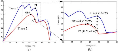
To show the effectiveness of the proposed circuit in recovering the power from the shaded modules, the PV system is switched from the bypass diode (mode) to the proposed circuit (mode). The eight modules are subjected to the following shading pat-terns: PV1=0.25 S, PV 2=0.25 S, PV3=0.5 S, PV4=0.7 S, PV 5=1.0 S, PV6=1.0 S, PV7=1.0 S, and PV8=1.0 S. The correspondingP–V curves for the bypass diode and the proposed method are simulated and are shown as trace 1 (blue) and trace 2 (red), respectively, in Fig. 12(a). As expected, using
Fig. 11 (a) Oscillogram from hardware of circuit in Fig. 9. Switching signal, S1, S3 (20 V/div), inductor current,iL1 (200 mA/div), inductor current,iL2 (200 mA/div), capacitor current,iC5(1 A/div). (b) Oscillogram from hardware of circuit in Fig. 9. Switching signal,S1, S3(20 V/div), PV output current,IP V (1 A/div), and PV output voltage,VP V(20 V/div).
the bypass diode, a multiple peakP–V curve is obtained. On the other hand, for the proposed circuit, the curve exhibits only a single peak because effectively, the modules are “balanced,” i.e. as if the partial shadings have not occurred. Also, note that this peak is much higher than the global peak of theP–V curve with the bypass diode.
Fig. 12. MPPT response when the PV system is switched from the bypass diode mode to the proposed method. (a) SimulatedP–Vcurve. (b) Experimental results.
TABLE II
CONDITIONS FOR THESTEPCHANGE INIRRADIANCE INSUN(S).Note: UNIT SUNEQUALS1000 W/m2ATSTC
Att1, the system is switched to the proposed circuit mode. From the simulation in Fig. 12(a), the peak moves to a new global point (63 V, 128 W) as pointed by P2 in theP–V curve. Experimentally, this movement can be observed in the oscillo-gram shown in Fig. 12(b). The P&O begins its tracking toward the new MPP (following the direction of the arrow) and finally settles at (61 V, 127.3 W). Thus, from this experiment, it can be concluded that by applying the proposed scheme, the out-put power is increased significantly, in this particular shading case by 36.8 W (29%). The slow tracking time is due to the small voltage step size of the P&O; if the step size is chosen to be larger, the tracking speed would be faster. However, this is achieved at the cost of larger steady state oscillation.
C. Rapid Change in Shading Patterns
Fig. 13 illustrates the response of the PV system with the by-pass diode when the irradiance pattern is changed very quickly. The shading patterns are depicted in Table II. Initially, the shad-ing patterns for the eight modules are subjected to Condition 1 of Table II. The correspondingP–V curve for this pattern is shown
Fig. 13 (a)P–V curve in bypass diode mode, with the shading condition shown in Table II. (b) Enlargement of (a).
Fig. 14. Dynamic response of the bypass diode mode with the shading condi-tion based on curves in Fig. 13.
in trace 1 of Fig. 13(a); for this case, the curve has four peaks. It is assumed that the PV is initially operated at a maximum point, P1 (48.2 V, 71.6 W). Note that, P1 is not the true global peak due to the fact that the P&O is already trapped at a local peak. When the irradiance is changed to Condition 2, the PV system is now characterized by trace 2. Under this condition, the curve consists of two peaks. For clarity, the enlargement of the PV curves is shown as an inset of Fig. 13(b). As can be observed, the change in the shading pattern forces the operating point to move from trace 1 to trace 2, i.e. the power drops from P1 and hits P2 (48.2 V, 41.6 W). From this point, the P&O algorithm starts the climbing process (to search for the peak) and finally settles at a new peak, GP3 (41.6 V, 57.2 W).
Fig. 15 (a)P–V curve for the proposed method with the shading condition shown by Table II. (b) Dynamic response of the proposed method for the curves in (a).
the MPPT controller is 100 ms, the P&O requires 25 cycles to complete the search for the new peak, i.e. from P1 to GP3.
Fig. 15 demonstrates the performance of the proposed method for a step change in irradiance, for the same conditions given in Table II. The correspondingP–V curve is shown in traces 1 and 2 of Fig. 15(a), respectively. Again, note that for the proposed method, the curve consists only of a single peak, which is advantageous with regards to MPPT implementation. Initially, due to Condition 1, the simulation maximum point is located at GP1 (65 V, 117 W). This point is also correctly shown in the oscillogram of Fig. 15(b), i.e. the oscillation is on average at (62 V, 115 W). When the shading condition is changed to Condition 2, the PV characteristic changes from trace 1 to trace 2; accordingly, the operating point moves from GP1 to GP2. The latter point is 63 V, 76 W. Experimentally, the step change in irradiance is introduced at time t1. As can be seen from the oscillogram in Fig. 15(a), the power drops to 74 W, while the voltage is maintained at approximately 62 V. Furthermore, since the proposed system does not have multiple peaks, GP2 is located directly below GP1 in theP–V curve. Consequently, even with a large step change in irradiance, the difference in the operating voltage between the two global peaks is very small. As a result, the P&O is able to track GP2 very quickly, i.e. within one to two MPPT control cycles, or 133 ms, as indicated in Fig. 15(b).
TABLE III
SHADINGPATTERNS.Note: CONDITION6IS FORBENCHMARKINGPURPOSE, i.e., NOPARTIALSHADING ISIMPOSED
From these observations, another important feature of the proposed method can be deduced: for the standard P&O, there is always a possibility that the algorithm will be trapped at the local peak. The inability to differentiate between the local and global peaks is a well-known drawback of the P&O algorithm [13], [17]. As such, more complicated MPPT algorithms (that can cater for partial shading), for example [6], [13], need to be considered. On the other hand, with the proposed technique, the global peak will always be tracked by a standard P&O because the multiple peaks simply do not exist. Being trapped at a local peak is not an issue.
D. Efficiency
To investigate the efficiency improvement of the proposed method, five irradiance patterns, representing various possible partial shading scenarios are simulated using a string of eight modules. These patterns are arbitrarily selected and are shown in Table III; they are labeled as Conditions 1 through 5. The efficiencies are benchmarked to the efficiency during the ab-sence of partial shading, i.e. Condition 6. For simplicity, four irradiation values, i.e. 1.0, 0.7, 0.5, and 0.25 S are used to repre-sent different levels of shading intensities (1.0 S=1.0 kW/m2). Again, the BP-MSX60 PV module is used. Each module is de-rated to 25 W at 35◦C, giving the total power (ideal) of 200 W
for the eight modules. For the validation, the experiment using the same simulation scenario is carried out. Furthermore, when the system is in the bypass diode mode, a semimanual control is applied for the MPPT algorithm to ensure that the operating point always matches the global peak. (Note: The P&O MPPT cannot consistently track the global peak under partial shading condition.)
Fig. 16. P–V curves generated by the proposed method and the bypass diode method (a) under Condition 2 and (b) under Condition 4 of Table III. (Note:Po1 is the maximum power achievable from the eight string for the bypass diode; Po2 is the maximum power achievable from the eight string for the proposed method.)
of the proposed system is computed as follows [45]:
η = Po
PSUM
(7)
wherePois the maximum output power delivered by the string,
i.e.IPV×VPV minus the converter losses, when the modules are subjected to the shading pattern.
For the nonshading condition (Condition 6, i.e. the bench-mark), the simulatedPSUMis 197.2 W. Since the P&O operates ideally,Po =PSUM. Consequently, the efficiency is 100%. Fur-thermore, because all modules are uniformly irradiated, neither the bypass diode nor the proposed circuit is activated. For other conditions (1 through 5), the efficiency varies according to the shading pattern imposed on the modules. For example, for Con-dition 2, the simulated efficiencies of the bypass diode and the proposed method are quite high (94 and 95%, respectively). This is because theirPois close toPSUM. Alternatively, this fact can be confirmed by plotting their correspondingP–V curves, as shown in Fig. 16(a). As can be seen, the peak power for bypass diode(Po1)is 147.2 W, while for the proposed method, the peak power(Po2)is 150.9 W. In another scenario, the shading pattern
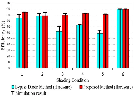
Fig. 17. Comparison of the system efficiency [as defined by (7)] of the bypass diode and the proposed method (simulation and experimental) for selected partial shading conditions.
imposed by Condition 4 results in a significant loss of power for the bypass diode (38.3 W). This causes its efficiency to drop to 75.3%. For the proposed method, the power loss is much lower (12.9 W); hence, its efficiency remains high, i.e. 93%. These facts can be related to the correspondingP–Vcurve, as shown in Fig. 16(b). Generally, the efficiency of the proposed method is relatively high, (i.e. above 90%), even in the case of severe shading, for example in Condition 5. The last row of Table IV computes the additional power that can be harvested (using the proposed method) to be part of the output power. This is the amount of power that is recovered from the shaded modules, which otherwise will be wasted if the bypass diodes are acti-vated. However, a generalized formula for the recovered power could not be easily quantified due to its dependence on a spe-cific shading pattern. However, from Table IV, in general, there is a consistent trend between the simulated and the experimental efficiencies. The agreement between the two can be further ob-served by the bar graphs in Fig. 17. From these correlations, two conclusions can be suggested: 1) the concept of energy recovery using the proposed method is verified and 2) the experimental rig (built using the tungsten–halogen bulbs) is adequate for the purpose of this study.
Another important point to note is that, for the bypass diode, it is assumed that the P&O successfully locates the global peak. In a real situation, this may not be necessarily the case. If the P&O is trapped at one of the local peaks,Pomight become much
lower and so does the efficiency. Hence, the computed efficiency shown in Table IV is actually the best possible case achievable for the bypass diode. On the contrary, for the proposed method,
Po is always unique because it has only one global peak.
There is another explanation why the total power that can be extracted by the proposed method could not reach the theoretical value ofPSUMunder partial shading: the low MPPT efficiency,
ηM PPT. Recall that the duty cycles of the switches are fixed at 50%. Since the circuit is opened-loop, under different irradiance, the voltage of every module could not be regulated toVM PP. To demonstrate this fact, a simulation is conducted using eight modules with shading conditions as shown in Table V. TheP–V
TABLE IV
SIMULATED ANDEXPERIMENTALRESULTS FORSHADINGPATTERNSIMPOSED ON THEBYPASSDIODE AND THEPROPOSEDCIRCUIT
(SIM: SIMULATION; EXP: EXPERIMENTAL)
TABLE V
CONDITIONS TOTEST THEDIFFERENCEBETWEEN THETRUE AND THE
OPERATINGMPP
Fig. 18. Operating point of each individual PV module for irradiance condi-tions given in Table V.
be seen, the operating point (i.e. the voltage of the PV) does not necessary match the true MPP. For example, for PV2, the true MPP is 17.2 V, while the operating point is only 15.38 V. Consequently, the power is reduced from 52.77 to 50.86 W. Similar reductions can be seen for other shading conditions. In overall, the reduction is reflected by the MPPT efficiency,
ηM PPT. In this case,ηM PPT is 96.5%.
From this illustrative example, it is acknowledged that for most shading conditions, the proposed circuit will yieldηM PPT
< 100. This is to be expected because a fixed duty cycle is employed for each switch. To ensure every module operates at its unique MPP, a closed-loop MPPT for every module must be employed, for example as proposed in [12]. However, to control every switch is costly because it needs additional mi-crocontrollers, sensors, and separate dc power supplies. As the number of modules gets larger, the complexity of the energy recovery circuit grows considerably; consequently, the system may no longer be practical. In addition, the individual switch needs to be synchronized with the MPP controller of the central inverter, thus losing its (flexible) retrofitting feature. Based on these considerations, it is more feasible for the proposed circuit to remain opened-loop. Despite this drawback, in most cases, the proposed circuit is very effective and is able to recover sub-stantial amount of energy during partial shading, as proven by the results shown in Table IV.
VI. CONCLUSION
improvement in the output power, especially under heavy par-tial shading condition. Experimental work has shown excellent agreement with the simulation. Experimental results show that using the scheme, the efficiency of the system can be increased up to 32%, compared to the bypass diode method. The improve-ment is more significant for the case of severe shadings. The extra power generated is expected to compensate for the cost of the extra components in the retrofit circuit and generates profit in the long run.
REFERENCES
[1] A. Maki and S. Valkealahti, “Power losses in long string and parallel-connected short strings of series-parallel-connected silicon-based photovoltaic modules due to partial shading conditions,”IEEE Trans. Energy Con-vers., vol. 27, no. 1, pp. 173–183, Mar. 2012.
[2] J. M. A. Myrzik and M. Calais, “String and module integrated inverters for single-phase grid connected photovoltaic systems—a review,” inProc. 2003 IEEE Bologna Power Tech. Conf., 2003, vol. 2, pp. 430–437. [3] H. Haibing, S. Harb, N. Kutkut, I. Batarseh, and Z. J. Shen, “A review
of power decoupling techniques for microinverters with three different decoupling capacitor locations in PV systems,”IEEE Trans. Power Elec-tron., vol. 28, no. 6, pp. 2711–2726, Jun. 2013.
[4] E. Koutroulis and F. Blaabjerg, “Design optimization of transformerless grid-connected PV inverters including reliability,”IEEE Trans. Power Electron., vol. 28, no. 1, pp. 325–335, Jan. 2013.
[5] L. Yanlin and R. Oruganti, “A low cost flyback CCM inverter for AC mod-ule application,”IEEE Trans. Power Electron., vol. 27, no. 3, pp. 1295– 1303, Mar. 2012.
[6] B. N. Alajmi, K. H. Ahmed, S. J. Finney, and B. W. Williams, “A maxi-mum power point tracking technique for partially shaded photovoltaic sys-tems in microgrids,”IEEE Trans. Ind. Electron., vol. 60, no. 4, pp. 1596– 1606, Apr. 2013.
[7] K. Kurokawa, H. Sugiyama, D. Uchida, K. Sakuta, K. Sakamoto, T. Ohshiro, T. Matsuo, and T. Katagiri, “Extended performance analy-sis of 70 PV systems in Japanese field test program,” inProc. 26th IEEE Photovoltaic Spec. Conf., 1997, pp. 1249–1252.
[8] Z. Salam and M. Z. Ramli, “A simple circuit to improve the power yield of PV array during partial shading,” inProc. IEEE Energy Convers. Congr. Expo., 2012, pp. 1622–1626.
[9] R. Kadri, J. P. Gaubert, and G. Champenois, “Nondissipative string current diverter for solving the cascaded DC–DC converter connection problem in photovoltaic power generation system,”IEEE Trans. Power Electron., vol. 27, no. 3, pp. 1249–1258, Mar. 2012.
[10] K. Ishaque, Z. Salam, and Syafaruddin, “A comprehensive MATLAB simulink PV system simulator with partial shading capability based on two-diode model,”Solar Energy, vol. 85, pp. 2217–2227, 2011. [11] C. R. Sullivan, J. J. Awerbuch, and A. M. Latham, “Decrease in
photo-voltaic power output from ripple: Simple general calculation and the effect of partial shading,”IEEE Trans. Power Electron., vol. 28, no. 2, pp. 740– 747, Feb. 2013.
[12] R. C. N. Pilawa-Podgurski and D. J. Perreault, “Submodule integrated distributed maximum power point tracking for solar photovoltaic applica-tions,”IEEE Trans. Power Electron., vol. 28, no. 6, pp. 2957–2967, Jun. 2013.
[13] K. Ishaque, Z. Salam, M. Amjad, and S. Mekhilef, “An improved particle swarm optimization (PSO) based MPPT for PV with reduced steady-state oscillation,”IEEE Trans. Power Electron., vol. 27, no. 8, pp. 3627–3638, Aug. 2012.
[14] T. Shimizu, O. Hashimoto, and G. Kimura, “A novel high-performance utility-interactive photovoltaic inverter system,”IEEE Trans. Power Elec-tron., vol. 18, no. 2, pp. 704–711, Mar. 2003.
[15] K Ishaque and Z. Salam, “A review of maximum power point tracking techniques of PV system for uniform insolation and partial shading con-dition,”Renewable Sustainable Energy Rev., vol. 19, pp. 475–488, 2013. [16] E. Koutroulis and F. Blaabjerg, “A new technique for tracking the global maximum power point of PV arrays operating under partial-shading con-ditions,”IEEE J. Photovoltaics, vol. 2, no. 2, pp. 184–190, Apr. 2012. [17] H. Patel and V. Agarwal, “Maximum power point tracking scheme for PV
systems operating under partially shaded conditions,”IEEE Trans. Ind. Electron., vol. 55, pp. 1689–1698, 2008.
[18] Z. S. H Taheri and K Ishaque, “A novel maximum power point tracking control of photovoltaic system under partial and rapidly fluctuating shadow conditions using differential evolution,” inProc. 2010 IEEE Symp. Ind. Electron. Appl., 2010, pp. 82–87.
[19] E. Bianconi, J. Calvente, R. Giral, E. Mamarelis, G. Petrone, C. A. Ramos-Paja, G. Spagnuolo, and M. Vitelli, “A fast current-based MPPT technique employing sliding mode control,”IEEE Trans. Ind. Electron., vol. 60, no. 3, pp. 1168–1178, Mar. 2013.
[20] S. Jing Jun and L. Kay-Soon, “Photovoltaic model identification using particle swarm optimization with inverse barrier constraint,”IEEE Trans. Power Electron., vol. 27, no. 9, pp. 3975–3983, Sep. 2012.
[21] A. K. Abdelsalam, A. M. Massoud, S. Ahmed, and P. Enjeti, “High-performance adaptive perturb and observe MPPT technique for photovoltaic-based microgrids,”IEEE Trans. Power Electron., vol. 26, no. 4, pp. 1010–1021, Apr. 2011.
[22] H. Guan-Chyun, I. H. Hung, T. Cheng-Yuan, and W. Chi-Hao, “Photo-voltaic power-increment-aided incremental-conductance MPPT with two-phased tracking,”IEEE Trans. Power Electron., vol. 28, no. 6, pp. 2895– 2911, Jun. 2013.
[23] K. Ishaque and Z. Salam, “A deterministic particle swarm optimization maximum power point tracker for photovoltaic system under partial shad-ing condition,”IEEE Trans. Ind. Electron., vol. 60, no. 8, pp. 3195–3206, Aug. 2013.
[24] M. Adly and A. H. Besheer, “An optimized fuzzy maximum power point tracker for stand alone photovoltaic systems: Ant colony approach,” in
Proc. 2012 7th IEEE Conf. on Ind. Electron. Appl., 2012, pp. 113–119. [25] N. Tat Luat and L. Kay-Soon, “A global maximum power point
track-ing scheme employtrack-ing DIRECT search algorithm for photovoltaic sys-tems,”IEEE Trans. Ind. Electron., vol. 57, no. 10, pp. 3456–3467, Oct. 2010.
[26] C. Huang-Jen, L. Yu-Kang, Y. Chun-Yu, C. Shih-Jen, H. Chi-Ming, C. Ching-Chun, K. Min-Chien, H. Yi-Ming, J. Yuan-Bor, and H. Yung-Cheng, “A module-integrated isolated solar microinverter,”IEEE Trans. Ind. Electron., vol. 60, no. 2, pp. 781–788, Feb. 2013.
[27] Z. Yan, L. Liming, and L. Hui, “A high-performance photovoltaic module-integrated converter (MIC) based on cascaded quasi-z-source inverters (qZSI) using eGaN FETs,”IEEE Trans. Power Electron., vol. 28, no. 6, pp. 2727–2738, Jun. 2013.
[28] G. R. Walker and P. C. Sernia, “Cascaded DC–DC converter connection of photovoltaic modules,”IEEE Trans. Power Electron., vol. 19, no. 4, pp. 1130–1139, Jul. 2004.
[29] L. Duo, Z. Zhe, X. Biwen, C. Min, and Q. Zhaoming, “A method of power decoupling for long life micro-inverter,” inProc. 37th Annu. Conf. IEEE Ind. Electron. Soc., 2011, pp. 802–807.
[30] R. S. Balog, K. Yingying, and G. Uhrhan, “A photovoltaic module thermal model using observed insolation and meteorological data to support a long life, highly reliable module-integrated inverter design by predicting expected operating temperature,” inProc. IEEE Energy Convers. Congr. Expo., 2009, pp. 3343–3349.
[31] Z. Qi, S. Xiangdong, Z. Yanru, and M. Mikihiko, “A novel topology for solving the partial shading problem in photovoltaic power generation system,” inProc. IEEE 6th Int. Power Electron. Motion Control Conf., 2009, pp. 2130–2135.
[32] C. Shih-Ming, L. Tsorng-Juu, Y. Lung-Sheng, and C. Jiann-Fuh, “A safety enhanced, high step-up DC–DC converter for AC photovoltaic module application,”IEEE Trans. Power Electron., vol. 27, no. 4, pp. 1809–1817, Apr. 2012.
[33] Z. Qian, H. Changsheng, C. Lin, A. Amirahmadi, N. Kutkut, Z. J. Shen, and I. Batarseh, “A center point iteration MPPT method with applica-tion on the frequency-modulated LLC microinverter,”IEEE Trans. Power Electron., vol. 29, no. 3, pp. 1262–1274, Mar. 2014.
[34] J. Shuai, C. Dong, L. Yuan, and P. Fang-Zheng, “Grid-connected boost-half-bridge photovoltaic microinverter system using repetitive current con-trol and maximum power point tracking,”IEEE Trans. Power Electron., vol. 27, no. 11, pp. 4711–4722, Nov. 2012.
[35] H. J. Bergveld, D. Buthker, C. Castello, T. Doorn, A. de Jong, R. van Otten, and K. de Waal, “Module-level DC/DC conversion for photovoltaic systems: The delta-conversion concept,”IEEE Trans. Power Electron., vol. 28, no. 4, pp. 2005–2013, Apr. 2013.
[36] K. Young-Ho, J. Young-Hyok, K. Jun-Gu, J. Yong-Chae, and W. Chung-Yuen, “A new control strategy for improving weighted efficiency in pho-tovoltaic AC module-type interleaved flyback inverters,”IEEE Trans. on Power Electron., vol. 28, no. 6, pp. 2688–2699, Jun. 2013.
phase-shift power modulation,” IEEE Trans. Power Electron., vol. 28, no. 6, pp. 2700–2710, Jun. 2013.
[38] G. R. Walker and J. C. Pierce, “Photovoltaic DC–DC module integrated converter for novel cascaded and bypass grid connection topologies; de-sign and optimisation,” inProc. 37th IEEE Power Electron. Spec. Conf., 2006, pp. 1–7.
[39] L. F. L. Villa, H. Tien-Phu, J. C. Crebier, and B. Raison, “A power elec-tronics equalizer application for partially shaded photovoltaic modules,”
IEEE Trans. Ind. Electron., vol. 60, no. 3, pp. 1179–1190, Mar. 2013. [40] I. Abdalla, J. Corda, and L. Zhang, “Multilevel DC-link inverter and
control algorithm to overcome the PV partial shading,”IEEE Trans. Power Electron., vol. 28, no. 1, pp. 14–18, Jan. 2013.
[41] G. Lijun, R. A. Dougal, L. Shengyi, and A. P. Iotova, “Parallel-connected solar PV system to address partial and rapidly fluctuating shadow condi-tions,”IEEE Trans. Ind. Electron., vol. 56, no. 5, pp. 1548–1556, May 2009.
[42] K. Ishaque, Z. Salam, and H. Taheri, “Simple, fast and accurate two diode model for photovoltaic modules,”Solar Energy Mater. Solar Cells, vol. 95, pp. 586–594, 2011.
[43] M. A. G. de Brito, L. Galotto, L. P. Sampaio, G. de Azevedo e Melo, and C. A. Canesin, “Evaluation of the Main MPPT techniques for photovoltaic applications,”IEEE Trans. Ind. Electron., vol. 60, no. 3, pp. 1156–1167, Mar. 2013.
[44] A. Dolara, R. Faranda, and S. Leva, “Energy comparison of seven MPPT techniques for PV systems,”J. Electromagn. Anal. Appl., vol. 3, pp. 152– 162, 2009.
[45] Z. Zhe, Z. Ouyang, O. C. Thomsen, and M. A. E. Andersen, “Analysis and design of a bidirectional isolated DC–DC converter for fuel cells and supercapacitors hybrid system,”IEEE Trans. Power Electron., vol. 27, no. 2, pp. 848–859, Feb. 2012.
Mohd. Zulkifli Ramli was born in Terengganu, Malaysia in 1978. He received the B.Sc. and M.Eng. degrees from the Universiti Teknologi Malaysia (UTM), Johor Bahru, Malaysia, in 2000 and 2004, respectively, all in electrical engineering. He is cur-rently working toward the Ph.D. degree at UTM in the area of photovoltaic.
He is currently a Senior Lecturer at the Univer-siti Teknikal Melaka, Melaka, Malaysia. His primary research interests include the hardware design of all power converters and their control systems.
Zainal Salam(M’99) received the B.Sc. degree in electronics engineering from the California State University, Chico, CA, USA, the M.E.E. degree in electrical engineering from the Universiti Teknologi Malaysia (UTM), Johor Bahru, Malaysia, and the Ph.D. degree in power electronics, from the Uni-versity of Birmingham, Birmingham, U.K., in 1985, 1989, and 1997, respectively.