A Comparison between Buck-Boost Inverter
with and without Buffer Inductor
Purwadi Agus Darwito
1, Soebagio
2, and Mauridhi Hery Purnomo
2AbstractThe electric vehicle inverter requires an induction motor drive with a high output of voltage and current to
reduce the number of batteries used and in turn reduce the vehicle’s weight. In this paper compared two single Phase Buck-Boost Inverter (SPBBI), that is between the SPBBI conventional topology with SPBBI new topology uses a buffer inductor. The results of comparison are expected that the new inverter topology can strengthen the voltage greater than the conventional inverter topology. The inverter’s components of capacitor and inductor were reconfigured. The circuit was simulated for various carrier and signal frequencies with various load. The simulation results of the proposed topology compared with the simulation results of conventional topologies commonly used in a variety of frequency and load values. It is shown that the output voltage and current can be strengthened significantly, with a value of more than five times of the output voltage compared to the conventional inverter. The new inverter topology is useful to be implemented for the electric vehicle.
Keywordsbuck-boost inverter, topology, buffer inductor, carrier frequency
AbstrakInverter yang digunakan pada mobil listrik dengan penggerak motor induksi harus mempunyai penguatan tegangan dan arus yang cukup agar jumlah baterai yang digunakan tidak terlalu banyak. Jumlah baterai berbanding lurus dengan berat mobil. Dalam penelitian ini dibandingkan dua buah inverter buck-boost satu fasa (SPBBI), yaitu antara SPBBI topologi konvensional dengan SPBBI topologi baru menggunakan induktor penyangga. Dari hasil perbandingan diharapkan inverter dengan topologi baru mempunyai penguatan tegangan output lebih besar dibanding inverter dengan topologi konvensional. Setelah ditetapkan nilai kapasitor dan induktor yang sesuai pada kedua topologi, dilakukan simulasi untuk beberapa frekwensi pembawa dan frekwensi sinyal dengan beban yang berbeda-beda. Hasil simulasi dari inverter topologi baru dibandingkan dengan hasil simulasi inverter topologi konvensional dalam beberapa nilai frekwensi dan beban yang berbeda. Hasil analisis menunjukkan bahwa penguatan tegangan output SPBBI topologi baru lebih dari lima kali tegangan inputnya dan arus outputnya lebih besar dibanding arus output inverter konvensional yang sudah ada
.
Inverter dengan topologi baru ini sangat cocok untuk mobil listrik.Kata Kunciinverter buck-boost, topologi, induktor penyangga, frekwensi pembawa I.INTRODUCTION6
n inverter is an electronic device to convert the DC input voltage into AC output voltage in adjustable size and frequency [1]. The inverter is applied in Uninterruptible Power Supply (UPS), active filter, and motor control [1–8]. It is divided into three topologies by comparing the output voltage to the input voltage. They are buck, boost, and buck – boost inverters. It is also grouped into three major groups of Voltage Source Inverter (VSI), Current Source Inverter (CSI) and Pulse Width Modulation (PWM).
In an electric vehicle, a DC voltage source either from dry battery or lead acid battery is converted into the AC output voltage using the inverter. The lead acid battery has a lower cost but heavier when compared to the dry battery. The heavier vehicle’s weight due to the battery requires a strong inverter. The electric vehicle’s motor also needs a capability to motion the electric vehicle at any given conditions such as constant speed, acceleration, or de-acceleration. The perfect inverter for the above conditions is buck–boost inverter because its output voltage can be adjusted when necessary.
Purwadi Agus Darwito is with Departement of Physic Engineering , Institut Teknologi Sepuluh Nopember, Surabaya, Indonesia. Email : [email protected].
Soebagio and Mauridhi Hery Purnomo are with Departement of Electrical Engineering, Institut Teknologi Sepuluh Nopember, Surabaya, Indonesia. Email : [email protected] ; [email protected].
Actually in the market is very difficult to get buck-boost inverter with specifications as needed for electric vehicle. Inverters are available most of the buck inverter ,or boost inverter with the strengthening of the output voltage is very small. Therefore need to be designed specifically buck-boost inverter for electric vehicle.
There were several buck–boost inverters suggested previously, such as those proposed by Caceres and Barbi [3]. The boost inverter achieves dc–ac convertion by connecting the load differentially across two dc–dc converter. These converters produces a dc-biased sine wave output, and modulating of one to the other by phase 180 degrees. The output voltage across the load R shows a pure sinusoidal waveform. Other researcher, [5] suggested a single phase buck-boost inverter with similar topology and working principle proposed by Caceres and Barbi. Their research resulted in the strengthening of the output voltage of about 2.5 times of the input voltage.
In this paper compared two Single Phase Buck-Boost Inverter (SPBBI), that is between the SPBBI conventional topology with SPBBI new topology. The new inverter topology is SPBBI with buffer inductor. It is developed from the conventional buck-boost inverter by adding a pair of inductor at the output terminal. The proposed topology then simulated and the results compared with the conventional topology that has been proposed by previous researchers. The simulation results are analyzed to obtain the output voltage and current characteristics. The proposed topology can provide the output voltage of more than five times of the input voltage.
II.METHOD A. Conventional Topology
Buck-boost Inverter conventional topology describe as figure 1. It is the kind of single-stage inverters with four switches are arranged through the frequency generated by the PWM or SPWM. Single-stage inverters are generally high efficient and low-cost, but usually suffer from limited power capacity.
The circuit have dc inputs of two identical boost dc-dc converter are connected in paralel with a dc source and the load is across the two outputs.
The buck-boost inverter can generates an ouput ac voltage lower or larger than the dc input voltage, depending on its duty cycle [1-8]. It is achieves dc to ac conversion as of two current bi-directional boost converters and the load is connected differentially across them. These inverter produce a sinusoidal voltage plus dc component of voltage on the capacitor. The modulation of each inverter is 1800 out of phase with
respect to the other.
The conversion process that occurs in the inverter are as follows : when switch S1 and S2 “ON”, switch S3 and S4 “OFF”, and vice versa [1-2]. For the first time, the DC input voltage source to cause an electric current in the loop I so happen charging inductor of La. Electric charge in the inductor La will be the current sources when the switch S3 and S4 “ON”, causing current flow in loop IV. The amount of charge depends on the duty cycle, so that the amount of strengthened also depends on the duty cycle. In the same way, when switch S3 and S4 “ON” there will be a process of charging the inductor Lb. Similar to the previous conditions, the electric charge on the inductor Lb causing electric current in the loop II. Conditions "ON" of pair of switch the turns will cause the current and voltage difference at both output terminals.
In a steady state with the application of Kirchoff's current and voltage laws on all the loops and the branch point when S1 and S2 switch are "ON", the equation can be derived as follows:
in
La
V
V
(1)Cb
Lb
V
V
(2)Lb Cb
o
i
i
i
(3)Ca Cb
o
V
V
V
.(4)
Substitution of Equation 3 and 4 resulted in following differential equation :
a Ca b Cb b Lb Cb RC V RC V C i dt V d ) ( (5)
Substitution of Equation 2 and 4 resulted in following differential Equation :
b Ca Cb b Lb b Lb
L
V
i
L
R
i
L
R
dt
i
d
(
)
(6)
Equation (5) and (6) can be written in the following matrix differential equation :
Ca Cb b b b Cb Lb b b b Cb Lb V i RC L L R V i RC C L R dt dVdt di 1 0 1 1 1
0 (7)
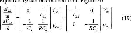
Using the same method, Equation 8 can be obtained from circuit when S3 and S4 switch “ON”.
Cb Ca a a a Ca La a a a Ca La V i RC L L R V i RC C L R dt dVdt di 1 0 1 1 1
0 (8)
B. Proposed New Topology
The proposed a new topology of single phase buck boost inverter with buffer inductor. Topological differences with the conventional topology is the addition of the inductor at the output terminal. Additional inductor position is more advantageous when compared with the conventional topology, because it helps keep the electrical charge at the loop more energized. With the addition of the inductor the output voltage is expected to be larger than the conventional topology. In testing, the output of the new topology will be compared with the output of the conventional topology.
Figure 2 shows a topology of single phase buck-boost inverter with buffer inductor were proposed. It consists of dc supply voltage Vin, two input inductor La1 and Lb1, two buffer inductor La2 and Lb2, four power switches IGBT S1-S4 are controlled by SPWM, two Capacitor Ca and Cb, and load resistance R.
C. Principles of Operation
The principle of SPBBI with buffer inductor can be explained through Figure 3a and 3b. When S1 and S2 “ON”, the equivalent circuit as shown in Figure 3a. On the other hand when the S3 and S4 “ON”, the equivalent circuit as shown in Figure 3b. To set the open and close switches S1 - S4, using SPWM method to set the sine control frequency and triangular carrier frequency. SPWM parameters are amplitude, frequency, phase angle, and duty cycle.
Inverter operating procedures are divided into several steps, namely:
The first steps : when S1 and S2 ON for the first time, the DC input voltage source to cause an electric current in the loop I so happen charging inductor of La1. The amount of charge depends on the duty cycle. Second steps : when S3 and S4 ON, the same as the previous step that the DC input voltage source to cause an electric current in the loop III resulting in the charging inductor of Lb1. At the same time in the loop IV also occurred electric current flow, because inductor La1 has been filled in the previous stage. Electric current in the loop IV is also causing the storage of electrical charge on the capacitor Ca. The third step: the same as the first step. Moreover at
The presence of current flow raises the output voltage between point A and point B.
The second and third step after another to produce a voltage and current output AC.
D. Modeling of SPBBI with Buffer Inductor
Inverter’s differential equation can be derived from
Figure 3 by determining the resistance value of R, the inductor of La1, La2, Lb1, Lb2, the capacitor of Ca and Cb. In a steady-state condition with the application of Kirchoff current and voltage Laws in Figure 3a for all loops and on branch point B, the equation can be derived as follows:
in
La
V
V
1
(9)Cb o
Ca
V
V
V
(10)Cb Lb
Lb
V
V
V
1
2
(11)
From Figure 3b it can be produced the following equation:
in
Lb
V
V
1
(12)Ca o
Cb
V
V
V
(13)Ca La
La
V
V
V
1
2
(14)Substitution of Equation 10 and 11 resulted in following equation:
1
2 Ca o Lb
Lb
V
V
V
V
(15) Voltage VLb1 is gained when S3 and S4 were “ON”,therefore Equation 15 became:
in o Ca
Lb
V
V
V
V
2
(16) From the branch point B at Figure 3b, under certain condition that current flowed through Lb1, it can be noted that:Lb Cb
o
i
i
i
(17) Equation 16 and 17 can be written in the following differential equation: Ca in b b Cb Lb b b b Cb Lb V V RC L V i RC C L dt dVdt di 1 0 0 1 1 1 1 0 2 2 (18)Equation 10 describes SPBBI with buffer inductor when switches S1 and S2 “ON”. As a comparison to SPBBI withoutbufferinductor, the equation be writte :
Using the same method at switch S3 and S4 “ON”, Equation 19 can be obtained from Figure 3b
Cb in a a Ca La a a a Ca La V V RC L V i RC C L dt dVdt di 1 0 0 1 1 1 1 0 2 2 (19)
III. RESULTS AND DISCUSSION
A simulator PSIM ver 9.0 was used to find out the characteristics both of the SPBBI with and without buffer inductor. The SPBBI is consisted of 5 batteries (type lead acid – 46B24L GS Battery Indonesia as
specified in Table 1) with Vin = 60 V, La1 = Lb1 = 0,5 µH, La2 = Lb2 = 15 µH, Ca = Cb = 65 µF, and load resistance R = 50 . The battery is assumed as an ideal voltage source, it is not reduced by a function of time. The purpose of the simulation is to determine whether the output voltage and current generated by the inverter is really shaped sinusoidal and stable. The intention is to know the shape of a sine wave generated completely smooth or ripple occurs. It is performed for different carrier frequencies, signal frequencies and various loads that may occur at an electric vehicle.
The first simulation performed to obtain the voltage and current waveform output function of time. Simulations performed for both types of inverters, which are using buffer inductors or not. In the inverter using buffer inductor, the value La1 = Lb1 = 5 µH and value La2 = Lb2 = 15 µH. As for the inverter without inductors buffer, the value of La = Lb = 20 µH.
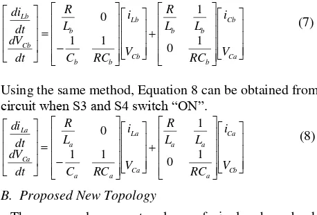
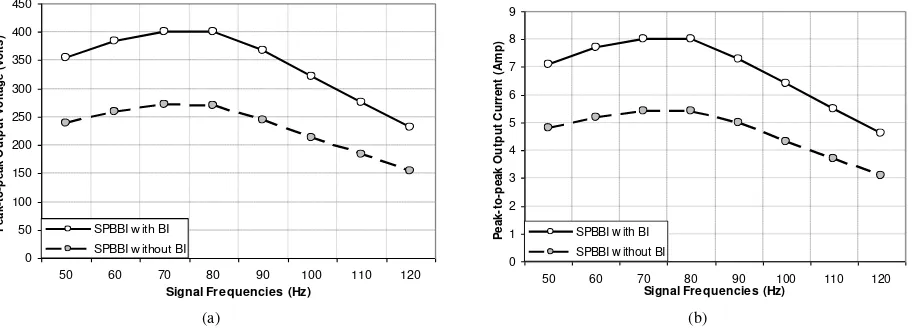
The signals frequency used in simulations ranging from 50 Hz to 120 Hz, because with a signal frequency below 50 Hz or higher than 120 Hz can not produce a truly sinusoidal output voltage and current. The carrier frequency used are between 3600 Hz to 6000 Hz. Inverter with carrier frequencies below 3600 Hz or above 6000 Hz does not produce a truly sinusoidal output voltage and current. Figure 4a and 4b shown the best output voltage and current for the SPBBI with and without buffer inductor. The each value of the carrier frequency, signal frequency, and load resistance R in Figure 4a and Figure 4b were 4000 Hz, 70 Hz, and 50 . The maximum voltage and cuurent results of simulation presented in Table 2. It is clear that the use of buffer can increase the output voltage and current.
The second simulation performed to obtain the curve of voltage and current output function of signal frequency. Figure 5a and 5b shown the output voltage and current for SPBBI with and without the buffer inductors based on changes in the signal frequency. Inverter with a buffer inductor at this frequency produces an output voltage (rms) were compared the input voltage is 272.2 Volt : 60 Volt or about 4.5 times.
IV. CONCLUSION
It has been proposed the SPBBI with buffer inductor to increase the output voltage and current. The proposed SPBBI can produce the output voltage more than five times of the input voltage. It is greater than produced by the SPBBI convensonal without buffer inductor. Therefore this proposed SPBBI with buffer inductor is very suitable when applied to a motor drive such as an induction motor as a driving force in an electric vehicle.
ACKNOWLEDGEMENTS
Figure 1. Conventional topology of single phase buck-boost inverter. Figure 2. Topology of single phase buck-boost inverter with buffer inductor were proposed.
(a) (b)
Figure 3. Equivalent circuit for : (a) S1 and S2 “ON” (S3 and S4 “OFF”); (b) S3 and S4 “ON” (S1 and S2 “OFF”)
(a) (b)
Figure 4. The output respon of the SPBBI with and without buffer inductor at carrier frequency 4000 Hz, signal frequency 70 Hz, and load resistive 50 : (a) voltage and (b) current
(a) (b)
Figure 5. The output response of the SPBBI with and without buffer inductor based signal frequency response from 50 Hz to 120 Hz : (a) voltage and (b) current
0 50 100 150 200 250 300 350 400 450
50 60 70 80 90 100 110 120
Signal Frequencies (Hz)
P
e
a
k
-t
o
-p
e
a
k
O
u
tp
u
t
V
o
lt
a
g
e
(
v
o
lt
s
)
SPBBI w ith BI SPBBI w ithout BI
0 1 2 3 4 5 6 7 8 9
50 60 70 80 90 100 110 120
Signal Frequencies (Hz)
P
e
a
k
-t
o
-p
e
a
k
O
u
tp
u
t
C
u
rr
e
n
t
(A
m
p
)
TABLE 1.
PHYSICAL DATA TYPE OF BATTREY 46B24L
Battrey Type Size
Dimension (mm) t x l x p 227 x 129 x 238
Capacity [Ah] 36
Discharge max [A] 150
Weight [Kg] 12.5
TABLE 2.
THE VOLTAGE AND CURRENT OF SIMULATION RESULTS
Voltage outputs (volts)
Current outputs (amperes) Peak-to-peak rms Peak-to-peak rms SPBBI with
BI 400.9 272.2 8.0 5.4
SPBBI
without BI 272.2 184.2 5.4 3.7
REFERENCES
[1] M.H. Rashid, “Power Electronics Circuits, Devices, and Application”, 2nd ed., Ptrentice-Hall International, Inc., London, 1993, pp. 356-411.
[2] P. A. Darwito, Soebagio, and M. H. Purnomo, “Single Phase Buck-Boost Inverter with Buffer Inductor using Power Simulator”, International Journal of Academic Research, Vol. 4 No. 3, May 2012.
[3] R. O. Cáceres and I. Barbi, “A boost dc-ac converter: analysis, design, and experimentation, IEEE Trans. Power Electron., vol. 14, pp. 134-141, January 1999.
[4] B. Koushki, H. Khalilinia, J. Ghaisari, N. M.Saghaian, “A New Three-Phase Boost Inverter : Topology And Controller”, CCECE/CCGEI May 5-7 2008 Niagara Falls, Canada, 2008.
[5] N. Vázquez, J. Almazan, J. Álvarez, C. Aguilar, and J. Arau,
“Analysis and experimental study of the buck, boost and buck-boost inverters”, in Proc. IEEE-PESC’99, June 27–July 1, 1999, Charleston, SC, USA, pp. 801-806
[6] J. Almazan, N. Vázquez, C. Hernandez, J. Alvarez J., and J. Arau., “A Comparison between the Buck, Boost and Buck-Boost Inverter”, IEEE, 2000.
[7] N. Vázquez, D. Cortes, C. Hernandez., J. J. Alvarez , J. Arau J., and Alvarez Jq., “A New Non- Linear Control Strategy for Boost Inverter”, IEEE, 2003.