Jisedai LSI oyo ni muketa koseino gurafen nanoribon debaisu haisen no tame no debaisu kozo oyobi zairyo dezain ni kansuru rironteki kenkyu
Bebas
103
0
0
Teks penuh
(2) Table of Content Figure List ........................................................................................................................ 1 Table List .......................................................................................................................... 4 Chapter 1: Introduction ..................................................................................................... 5 1.1 Overview of LSI technology................................................................................... 5 1.2 Significance of graphene and its challenges ......................................................... 10 1.3 Structure and Material Design in Graphene Electron Device ............................... 18 1.3.1 Previous Work on Graphene Device Structure Modification ........................ 18 1.3.2 Previous Work on Graphene Interconnect Material Design .......................... 20 1.4 Motivation of Thesis ............................................................................................. 22 Chapter 2: Theoretical Framework ................................................................................. 23 2.1 Introduction of theoretical method........................................................................ 23 2.2 Semi Classical Monte Carlo Particle Simulation .................................................. 23 2.2 First-principle theory calculation .......................................................................... 31 2.2.1 Basic of Quantum mechanics ......................................................................... 31 2.2.2 Density Functional Theory ............................................................................. 33 2.3 Molecular Dynamics ............................................................................................. 34 Chapter 3: High Speed Properties in Modulation Channel Width (MCW) GFET ......... 37 3.1 Introduction of Chapter 3 ...................................................................................... 37 3.2 Overshoot velocity effect in short-channel FET ................................................... 37 3.3 Design Principle of MCW-GFET ......................................................................... 40 3.4 Simulation Model of MCW-GFET for High Speed Enhancement ....................... 41 3.4.1 Simulated Device Structure ............................................................................ 41 3.4.2 Quasi 3D Poisson solver ................................................................................ 42 3.5 Result and Discussion ........................................................................................... 45 3.5.1 Electric Field Profile (MCW-GFET W= 0.1, W= 0.3) ................................. 45. i.
(3) 3.5.2 Mean Carrier Velocity (MCW-GFET W= 0.1, W= 0.3)................................ 49 3.5.3 MCW Effect in Monolayer and Bilayer Graphene Channel .......................... 52 3.6 Conclusion of Chapter 3 ....................................................................................... 55 Chapter 4: Bandgap Opening in Modulated Channel Width (MCW) GFET ................. 56 4.1 Introduction of Chapter 4 ...................................................................................... 56 4.2 Graphene Nanoribbon (GNR) ............................................................................... 57 4.3 Bandgap Calculation (10 nm GNR, Bilayer Graphene) ....................................... 57 4.4 Result and Discussion ........................................................................................... 60 4.4.1 Mean Velocity Profile (MCW-GFET, Bilayer GFET, GNR FET) ................ 60 4.4.2 MCW Effect inside the Device Channel ........................................................ 62 4.5 Conclusion of Chapter 4 ....................................................................................... 67 Chapter 5: Stability of Intercalated GNR ....................................................................... 68 5.1 Introduction of Chapter 5 ...................................................................................... 68 5.2 DFT Simulation Model (GNR width N=10, N=20, Br 3%, 9%) .......................... 69 5.3 MD Simulation Model (GNR width 3nm, 10 nm, Br 15%, 30%) ........................ 71 5.4 Conclusion of Chapter 5 ....................................................................................... 78 Chapter 6: Thesis Conclusion ......................................................................................... 80 6.1 Thesis contribution ............................................................................................... 80 6.2 Future works ......................................................................................................... 81 6.2.1 MCW-GFET................................................................................................... 81 6.2.2 GNR Intercalation .......................................................................................... 82 Acknowledgement .......................................................................................................... 84 REFERENCE ................................................................................................................. 85. ii.
(4) APPENDIX .................................................................................................................... 93 A-1. Structure Optimization (W, Modulation Region, Modulation Length) .............. 93 A-2. Channel design to reduce quantum reflectance effect ........................................ 96 A-3. Current and Voltage characteristic inside MCW-GFET .................................... 98. iii.
(5) Figure List Fig. 1: Scaling down and performance enhancement in LSI technology Fig. 2: 14 nm technology node of a Fin-Field Effect Transistor developed by Intel Fig. 3: ITRS roadmap for the current density of Copper (Cu) Fig. 4: Increasing resistivity of Cu interconnect with width of <100nm Fig. 5: ITRS roadmap of technological advancement and development Fig. 6: Graphene structure as a unit that can formed fullerene and CNT. Fig. 7: E-k dispersion of graphene showing zero bandgap Fig. 8: Bandgap opening, Eg inside GNR. Eg is inversely propotional to GNR width. Fig. 9: Armchair and zigzag edge in GNR. The edge states affect the semiconducting and metallic properties in GNR Fig. 10: Performance in terms of carrier mobilitiy (300 K) as a function of energy gap of materials to replace silicon in conventional CMOS Fig. 11: Simulation result of the resistivity in single-layer GNRs of different edge states (a- armchair, z-zigzag) an MFP of 1 μm compared with those of copper wires and SWNT bundles Fig. 12: Suspended graphene device which show high carrier mobility since SiO2 surface scattering is absent Fig. 13: (a) Structure of Graphene Nanomesh (GNM) transistor where mesh are fabricated to induce bandgap inside graphene channel. (b) SEM image of a GNM device made from nanomesh with a periodicity 39 nm and neck width of 10 nm. Scale bar, 500 nm Fig. 14: Monte carlo simulation flow that is ued to estimate the properties of devices in this studies Fig. 15: Device Dimension Fig. 16: Potential difference in meshes Fig. 17: Monte Carlo Flow Chart which include drift and scattering event of carriers Fig 18: LJ pair potential that make use of the repulsive and attractive interaction between 2 atoms or molecules. 1.
(6) Fig. 19: Morse potential includes the disassociation energy between two atoms Fig. 20: Velocity overshoots effect in Silicon Fig. 21: Velocity overshoots effect in Graphene FET Fig. 22: HEMT with nonuniformed channel structure. Average velocity of the transistor in such channel increase Fig. 23: Modeled device structure Fig. 24: Charge confined in a nonuniform cubic Fig. 25: Electric Field in MCW-GFET with a bilayer graphene channel Fig. 26: Electric Field in MCW-GFET with a monolayer graphene channel Fig. 27: Full Electric Field profile in MCW-GFET and Conventional GFET with a monolayer graphene channel. Local stronger electric filed is introduced at the modulated region Fig. 28: Mean carrier velocity in MCW-GFET with bilayer graphene channel. Modulated region transit time, τ* is the transit time at the source side of the channel Fig. 29: Mean carrier velocity in MCW-GFET with monolayer graphene channel. Modulated region transit time, τ* is the transit time at the source side of the channel. Fig. 30: Energy profile in MCW-GFET with bilayer graphene channel Fig. 31: Energy profile in MCW-GFET with monolayer graphene channel Fig. 32: GNR array introduced in the modulated region of the graphene channel Fig. 33: Unit cell of GNR Fig. 34: Unit cell of Bilayer Graphene with a perpendicular electric field being applied Fig. 35: Bandstructure of a 10 nm GNR Fig. 36: Bandstructure of a Bilayer Graphene with a 1.2 V/nm electric field being applied perpendicularly Fig. 37: Transport characteristic of 4 Different devices is being estimated which each devices having a bandgap of 100 meV except for in Conventional GFET Fig. 38: Velocity profile in MCW, Bilayer, GNR, and Conventional GFET. 2.
(7) Fig. 39: Spatial distribution of the velocity of the carrier inside the devices. The dots represent carriers inside the device. The circle and the arrow illustrate the velocity vector inside the channel. Fig. 40: Schematics of band structures and working principles of (a) conventional GFET (b) MCW-GFET (c) GNR-FET Fig. 41: Profiles of average lateral components of carrier velocity (vx) of modulation channel width graphene FETs (MCW-GFETs) and parallel graphene nanoribbon FETs (GNR-FETs) with 50-nm and 100-nm channels Fig. 42: Transit time of devices calculated in this work compared with previous work on InP HEMT (experimental) Fig. 43: Staging phenomenon in graphene intercalated with bromine.The same model is used with fewer number of Br and graphene layers Fig. 44: Simulated model of a single bromine (red) in bilayer GNR (3 nm width) Fig. 45: Post simulation structure of 3 nm width GNR with 15% Br intercalation Fig. 46: Post simulation structure of 10 nm width GNR with 15% Br intercalation Fig. 47: Post simulation structure of 3 nm width GNR with 15% Br intercalation Fig. 48: Intercalated structure models in graphite intercalation. Stage 1-4 depends on the type and quantity of the intercalation compound Fig. 49: Stability of calculated intercalation structure in both ab-initio and MD calculation Fig. A1: Transit time of Bilayer MCW-GFET with various modulation region and length Fig. A2: Transit time in MCW-GFET with various W (bilayer channel) Fig. A3: Transit time in MCW-GFETs with different design where gradual design is being considered to lower the effect of quantum reflectance Fig. A4: Drain current vs topgate voltage in MCW-GFET and conventional GFET. 3.
(8) Table List Table 5-1: Summary of MD simulation Table 5-2: Summary of DFT simulation. 4.
(9) Chapter 1: Introduction 1.1 Overview of LSI technology High integration of LSI technology has led to miniaturization or down scaling of the electronic components has given a big impact on the semiconductor technology in this past 40 years. This down scaling trend is very feasible since we are able to achieve not only device with higher performance, but also lower production cost as larger number of transistors can be occupied per chip. This long trend which started since 1970 is called ‘Moore’s Law’, where the number of transistors per chip is estimated to double every year by scaling down the size of transistors [ 1 , 2 ]. However, this trend of downscaling is reaching its limit in both transistors [ 3 , 4 , 5 ] and interconnects technologies [6]. In conventional silicon devices, as the gate-length becomes too short, problems such as short-channel effects [7, 8, 9] occur. The main problem is that short channel contributes to off-leakage current due to the tunneling behavior of the electrons. To date, we have a 14 nm node technology by Intel where the physical gate length is actually speculated to be shorter than 14 nm. In regards with the ‘technology nodes’, it is expected that there will be only another three generations of them after the current 14 nm generation. Expected to be in 2020, when the gate-length is down to 5 nm, marks the limit of CMOS technology where there will be too huge off-leakage current in the entire chip [3].. 5.
(10) Fig. 1: Scaling down and performance enhancement in LSI technology. Fig. 2: 14 nm technology node of a Fin-Field Effect Transistor developed by Intel [10] 6.
(11) On the other hand, together with the down scaling of the silicon transistor, conventional copper interconnects is also reaching its limit [6, 7] because of the high integration in LSI technology. By the year 2020, it is predicted that the interconnect wire width will be as narrow as 22 nm while current density reaching 5.8 × 10⁶ A/cm2 [ 11 ]. The current-carrying capability of conventional copper interconnect cannot achieve such high current density due to limiting factors such as carrier scattering at material interface/grain boundaries, thermal induced failure and electromigration [12,13]. Moreover, aggressive scaling of copper interconnects will further increase energy loss through heat dissipation which is governed by higher resistance in narrower interconnects [14]. Although past predictions are not always correct, with the way the trend is continuing right now, we expect the both conventional transistor and interconnect technology will struggle to stay alive in another 10-20 years.. Fig. 3: ITRS roadmap for the current density of Copper (Cu) [15] Reprinted and modified with permission from ITRS 2013 Edition, Interconnect, Figure INTC9. 7.
(12) Fig. 4: Increasing resistivity of Cu interconnect with width of <100nm [16]. A solution to this struggle is the adoption of new device structure such as the double gate (DG) [17] or fin-FET [18] type MOSFETs. These devices are excellent in suppressing the off-leakage current. Another application is Si-nanowire [19] MOSFETs which show higher on-current conduction than conventional DG FETs and the fact that they can be adopt for high-density integration is yet really attractive. Despite of these new technologies, the ultimate question is what will come next after reaching the final limit of downsizing? In order to answer this question, some suggest that a new prominent material is needed to replace the conventional silicon channel and copper interconnects technology. Amazingly a single material has the potential to solve these two crucial technologies and is very promising for the future of higher performance electron devices. These new materials are considered as an ‘Emerging Material’ by the ITRS. In order to keep the Moore’s law trend going the advancement in current LSI technology can be generally divided into two major parts. First is the trend of device miniaturization that we discuss earlier, which is called ‘More Moore’. The second part is something referred to as ‘more than Moore’ where intensive works is being carried on to achieve something that exceeds the current trend. ‘More Moore’ defined by the International Roadmap of Semiconductors (ITRS) indicates something we refer as. 8.
(13) ‘Beyond CMOS’ This includes researches on new materials, which are commonly addressed as Emerging Research Materials (ERMs) as an alternative channel material for extending CMOS. These ERMs includes graphene [ 20 ], carbon nanotube (CNT) [ 21 ] and semiconductor nanowires [22, 23] which are excitingly able to enhance the performance of MOSFETs while possibly reducing the power consumption because of their properties. Higher carrier mobility in III-V, Ge, graphene, carbon nanotube for example can provide higher on currents, Ion and lower gate capacitance at constant Ion. However issues need to be addressed before such materials can be integrated in the current CMOS technology.. Fig. 5: ITRS roadmap of technological advancement and development [24]. Reprinted with permission from ITRS 2013 Edition, Emerging Research Device, Figure ERD1. 9.
(14) 1.2 Significance of graphene and its challenges One of the most promising materials to solve both the issues that we have in transistors and interconnects is graphene. Although graphene has just recently discovered in 2004 and its evaluation is still at early stage, its extraordinary characteristics attract many research works and its discovery was awarded the Noble prize. Graphene is a nanocarbon material where atoms of carbon are being bonded together forming a sheet of honeycomb lattice structure as shown in Fig. 6. It is like an unzipped version of a CNT. 3D-stacking of graphene layers formed the well-known graphite. Although it is considered that 100 layers of a 2D sheet material such as graphene stacked together can be considered as a thin film to a 3D material such as graphite, it has been found that graphene is reaching the 3D limits of graphite at 10 layers [25]. Carbon atoms inside graphene are being bonded to each other by a sp2 bonding, leaving unbounded п-orbitals. These п-electrons can act as high mobility carriers which contribute to amazing properties inside graphene. Among these amazing properties is massless Dirac fermions in graphene which yields a carrier mobility of up to 200 000 cm2/Vs and a carrier velocity of up to ~106 m/s [26], linear E-k dispersion and ballistic transport. This extraordinary high mobility is 100~1000 times higher than that of silicon in conventional transistor. Owing to these exceptional properties, graphene shows potential for both transistor and interconnect application. Moreover, graphene ambipolar characteristic and its similar p and n carrier velocity make it possible for graphene to serve as both p-channel and n-channel material. Graphene also has a high aspect ratio which makes it immune to short channel effect which is one of the main problems in conventional silicon LSI applications. Despite having these amazing properties, Graphene is however a zero bandgap semiconductor. Thus, this is a very significant issue that is commonly addressed by researchers to be solved before graphene can be used for extended CMOS applications. Nevertheless, ways of creating a bandgap are being previously reported [27, 28, 29]. When graphene was first discovered in 2004, graphene was exfoliated or peeled off from graphite using a scotch tape. This method of producing graphene is called exfoliation method and researchers all over the world initially use this method to produce high quality graphene flakes. The graphene flakes produced defer in specimen. 10.
(15) size since it is impossible to control the size of graphene peeled using this exfoliation method. Since the size of graphene cannot be controlled, although high quality graphene can be produced this way, such method is not suitable for mass production in graphene and surely cannot be adopted inside the current LSI fabrication process. Graphene can also be synthesized on Silicon Carbide (SiC) with annealing process where temperature and SiC surface control can produce high quality graphene as well as being able to control the number of graphene layer produce. The major drawbacks of this process is still however not compatible with conventional LSI fabrication process since the annealing temperature is very high (1000 ˚C). Another way to produce graphene is by Chemical Vapor Deposition (CVD) where graphene is grown on Cu films. Graphene with large grain size and high in quality can be grown using this method. However, similar to graphene synthesis on SiC, although graphene can also be grown at low temperature which is compatible with LSI fabrication process (logic application, 400450 ˚C, flash memory, 650 ˚C), high CVD temperature is needed in order to produce high quality graphene.. Fig. 6: Graphene structure as a unit that can formed fullerene and CNT. This is modified from[25]. 11.
(16) Fig. 7: E-k dispersion of graphene showing zero bandgap. Despite the setbacks in graphene production, developments on graphene electron devices have been very intensive. For example, graphene FETs (GFET) with promising high cut-off frequency have been previously reported. In 2010, Y. M. Lin from IBM group and L. Liao et al. both respectively reported a graphene FET (GFET) with a cut-off frequency of 100 GHz [30] and 300 GHz [31]. This value is comparable to of a GaAs high electron mobility transistor with similar gate length. K. Kim et al. also reported a GFET with a cutoff frequency of 80 GHz on the same year. Although the GFET report by K. Kim had a lower cutoff frequency and larger gate length, CVD graphene was used for the fabrication process [32]. In 2012, another breakthrough was reported by Y. M. Lin group with a GFET of 350 GHz [33]. L. Leio group however reported the best GFET on the same year with a cutoff frequency of 457 GHz [34]. With this, advancement in GFET fabrication is catching up with the development of high speed III-V semiconductor at a very fast pace. Despite this kind of achievement, the future of graphene electronics is yet still challenging. In most of the reports, where graphene devices were fabricated on a standard silicon wafer with a silicon dioxide insulator layer, the electrical properties of the graphene channel deteriorated showing lower performance in terms of the carrier mobility comparing to their theoretical values. There are suggestions that these findings were caused by parasitic factors such as the. 12.
(17) surface scattering of SiO2 [35] or by damage of graphene flakes during fabrication process. To solve this issue alternate substrates are used replacing silicon substrate such as Boron Nitride (BN) substrate which possesses an identical lattice structure with graphene. In this case the carrier mobility was reported to be enhanced [36]. The feasibility of this BN substrate or layer to be integrated with CMOS technology is however still being evaluated and BN substrate itself is rather costly. As stated briefly earlier, graphene lacks a very essential property for switching device application; a bandgap. Graphene exhibits a linear E-k dispersion with no bandgap. Nevertheless, ways such as by producing a thin graphene stripe called graphene nanoribbon (GNR) or by applying a perpendicular electric field to a bilayer graphene channel were reported to be able to create a bandgap. Although Bilayer GFET with perpendicular electric field showed an excellent device with high on-off current ratio and a saturated current, the problem with this device is its complex structure that is very difficult to be used as a building block in integrated circuit. In that sense, GNR is a better candidate for graphene-based logic applications. Bandgap opening in GNR is induced by quantum confinements. In this quantum confinement effect, electrons occupy quantum well states which are discrete enabling a quantumly confined bandgaps. This phenomenon is shown in First Principle theory calculation where the size of the bandgap opening inside GNR was found to be inversely proportional to its width [28]. Due to this substantial bandgap opening, FETs with GNR channels show reduced off-leakage current and a larger on-off current ratio with a current saturation. Experimental and theoretical studies both show that GNR-FETs or GNR-tunneling FETs (GNR TFETs) with sub-10 nm GNR channels can produce a substantial band gaps with Ion/Ioff ratios of higher than 106 achieved [37]. Another interesting application using GNR is GNR TFET which shows a subthreshold slope of 13 meV/dec [38] and has an advantage over the 60 meV/dec in conventional MOSFET making use of the tunneling effect.. 13.
(18) Fig. 8: Bandgap opening, Eg inside GNR. Eg is inversely propotional to GNR width. P1-P4, D1-D2 are different samples measured in this work. Reprinted with permission from [29]. Copyright by the American Physical Society.. However, one of the main challenges with GNR FET is to produce a smooth GNR down to 10 ~ 20 nm channel width where the size of bandgap opening is substantial. Conventional lithography and etching methods have been used to fabricate GNR FET with such channel width from both exfoliated graphene [39] and CVD graphene [40]. In this method, graphene edges cannot be fully controlled and defects or edge disorders have always been inevitable. These parasitic factors undermined the performance of GNR where devices show lower carrier mobility. In such cases, the bandgap opening is suggested to be dominantly arising from transport gap between localized states induced by the disorder instead of the quantumly confined bandgap. Therefore, cutting edge etching and fabrication technology needed to be properly developed to solve such issue in the near future. On the other hand, chemical unzipping of CNT [41, 42] enables production of GNR with smoother edge. When unzipping CNT, different chemicals were used in different previous works to break the bond. 14.
(19) between carbon atoms and unzipped CNT into GNR. To prevent oxidation of produced GNR which is common after chemical unzipping process of CNT, 3 steps annealing process in [41] was introduced. Moreover, argon plasma etching had also been used to unzip CNT into GNR [43]. GNR with controlled edge without any disorder can also be synthesized by growing it directly on SiC substrates using ion implantation and laser annealing [44]. Although these bottom-up methods can produce GNR with smoother edges, it is not reproducible and still not compatible with conventional LSI technologies. It is known that the edge state of GNR largely affects its characteristic. GNR conductivity changes drastically in zigzag or armchair edge as shown in Fig. 8. Generally, it is semiconducting in an armchair GNR (A-GNR) while zigzag edged GNR (Z-GNR) shows metallic properties. Theoretical prediction also shows that A-GNR can also be metallic and Z-GNR can be semiconducting. In the case of A-GNR, the dimer N, number or atoms forming the GNR width affects its characteristic. It is found that the characteristic differs in 3 different ways 3N, 3N+1 and 3N+2 [28]. A-GNRs with 3N and 3N+1 dimer are semiconducting while ones with a dimer of 3N+2 are metallic. ZGNRs on the order hand show bandgap opening in GNR width of lower than 7 nm due to edge magnetism. This property has been found in both theoretical and experimental studies [45]. While the most stable structure of GNR edge is when it is being terminated with hydrogen atoms, terminations of the edges with other atoms or modulations of the edge states change GNR electronic band structure. Because of such effects, researchers strategically modulate the edge and width in different ways. These methods include applying disorder [46], doping [47], or mechanical strain [48].The main disadvantage of GNRFET is that, the drift current is significantly lower because of the nano-scale dimension of its width [49]. The mobility in GNR FETs are also lower because of the bandgap opening. Mobility and bandgap introduction of graphene and other materials from previous work is being summarized in Fig.10.. 15.
(20) Fig. 9: Armchair and zigzag edge in GNR. The edge states affect the semiconducting and metallic properties in GNR.. Fig. 10: Performance in terms of carrier mobilitiy (300 K) as a function of energy gap of materials to replace silicon in conventional CMOS [50]. Reprinted with permission from [51]. Copyright by IEEE.. 16.
(21) On the other hand, researches on graphene interconnects have also been done intensively. Both wide graphene ribbon [ 52 ] (>100 nm) and graphene which is fabricated into narrow-width [53] (<100nm) graphene nanoribbon (GNR) have been systematically studied and compared to conventional copper interconnect. Multilayer graphene is a better candidate for the used in interconnect application due to its lower resistance. It has shown both an interesting temperature coefficient [ 54 ] and a theoretical projection that outperforms Cu as in interconnect applications [55]. In width of shorter than 8 nm, the resistance per unit length of GNR is surprisingly lower than that of Cu [56]. Morever, GNR interconnect shows an impressive breakdown current density in graphene wire which was reported by R. Murali et al. [54]. Initially, multilayer graphene interconnects are exfoliated from highly oriented pyrolytic graphite (HOPG) and kish graphite which is not suitable for large-scale manufacturing. In 2011, CVD-grown multilayer graphene has also been reported and the resistivity is lower prior to other researches [56].. However, despite all this promising data, the lowest. value reported from experimental works for GNRs resistivity is still two and three times higher than copper wires. It is suggested this high resistivity mainly resulted from edge roughness scattering in GNR [54].. Fig. 11: Simulation result of the resistivity in single-layer GNRs of different edge states (a- armchair, z-zigzag) an MFP of 1 μm compared with those of copper wires and SWNT bundles.[57] Reprinted with permission. Copyright by IEEE.. 17.
(22) 1.3 Structure and Material Design in Graphene Electron Device 1.3.1 Previous Work on Graphene Device Structure Modification In order to solve these challenges in the realization of graphene electron devices discussed in the previous sub chapter, some important works tackle these issues by modifying the structure of graphene devices. To suppress surface scattering of SiO2 for example, a new GFET structure is reported by suspending the graphene channel in a device called suspended GFET. In this structure, the graphene is literally being suspended like a bridge between the source and drain of the channel without being on any SiO2 surface. In this device, the carrier mobility of the device improved significantly and a similar value with the theoretical value can be obtained [58]. This structure is however mechanically unstable making it vulnerable of being damaged by a slight external force or a high current flow [59]. To deal with the lack of a bandgap an low current coupled with a low carrier mobility in GNR FET, in 2010, by modifying the physical structure of graphene, J Bai et al. introduce a new structure called graphene nanomesh (GNM) where bandgap opening is possible [60]. Although device current is usually low in GNR device because of the narrow channel, in GNM transistor, the current is not compromised because of the bandgap opening where a GNM device shows a nearly 100 time higher current than individual GNR device with similar bandgap opening. However, the conductivity of GNM transistor is ~1-2 orders of magnitude lower than of bulk graphene. Apart from physical modification, chemical modification can also open a bandgap in graphene. These modifications include partially oxidizing graphite [61] or by reducing graphene oxide [62], GO until a graphene like behavior is achieved is such cases. Other chemical modifications are hydrogenation of graphene basal plane [63], fluorination [64] and chemical doping [65]. Despite these breakthroughs, graphene-based device conductivity decreases as bandgap is opened up because of the mass is heavier and the E-k dispersion is flatter when the bandgap is enabled.. 18.
(23) Fig.12: Suspended graphene device which show high carrier mobility since SiO2 surface scattering is absent. Reprinted with permission from [59]. Copyright by Elsevier.. Fig.13: (a) Structure of Graphene Nanomesh (GNM) transistor where mesh are fabricated to induce bandgap inside graphene channel. (b) SEM image of a GNM device made from nanomesh with a periodicity 39 nm and neck width of 10 nm. Scale bar, 500 nm. Reprinted with permission from [61]. Copyright by Nature.. 19.
(24) 1.3.2 Previous Work on Graphene Interconnect Material Design As discussed earlier, although graphene has a longer mean free path (MFP) than Cu, the Line Edge Roughness (LER) scattering increase the resistivity of GNR making it larger than Cu. The issue of this LER scattering is becoming more important in narrower GNR that is needed for future LSI applications. A way to reduce the resistivity in GNR is by doping. The motivation is to tailor the electronic properties by shifting the fermi level in GNR as a result of the doping effect. This will later lead to higher carrier density in graphene interconnects and a lower resistivity [66]. In 2010, a group reported that, by doping graphene with AuCl3, they successfully reduced the resistivity of graphene by 77%. Other works also shows that the Fermi level of graphene can be controlled by doping. Depending on the dopant that is used the type of doping is decided whether it is a p-type doping or an n-type doping [67, 68, 69]. However, such that has been actively done to achieve doping effect in graphite to lower its resistivity [70], a better way of doping graphene in order to shift the fermi level without largely reducing the conductivity of graphene is by intercalation as chemical doping that is discussed earlier can affect the structure of graphene lattice by substitution doping [71]. Moreover, intercalation is better since multi-layer graphene can be doped this way. Intercalation is a method where intercalation compounds are inserted between the layers of graphene. The interlayer distance in graphite or graphene will significantly increase depending on the nature of the intercalation compound and this affects the electronic coupling between the layers which will then changing its property. Intercalation is a better way of doping since the structure of an intercalated graphene host is not largely change since intercalation compound does not bond with the carbon atoms in an intercalation process. Since the 1980s, intercalation of atoms such as alkali metals, halogens, oxygens and hydrogens has been reported by several groups and it is shown that resistivity is reduced in intercalated graphite [72, 73, 74]. Recently, several works on few layers and multi-layer graphene intercalations have also been done showing enhance resistivity and doping effect [75, 76]. For interconnect applications, intercalation of GNR wire is inevitable. Although there is a breakthrough of intercalating GNR which show a low resistivity, little is known on the stability of the intercalated GNR structure. In the case of graphite, there are cases where the intercalation compound escapes from the graphene over time 20.
(25) [77] leading to the resistivity of the graphite to increase again. There is also still a need to determine the most feasible candidate to be used as an intercalation compound with regards to its stability. Instability of an intercalated graphene host can also lead to the peeling of graphene flakes [78] which will deteriorate the intercalation structure.. 21.
(26) 1.4 Motivation of Thesis The purpose of this research is to propose ways to solve the issues involving Graphene Electron Devices focusing on GFET and graphene interconnect by the approach of redesigning the graphene device structure and material. To start with, our first objective is to propose a novel GFET structure in order to enhance the high speed property inside graphene channel. This new GFET architecture will make use of the overshoot velocity nature of carrier in graphene channel to enhance the carrier velocity inside the channel achieving faster transit time. Our second objective is to focus on an extended version of the new design, making use of quantum confinement of GNR in order to achieve a bandgap opening inside our graphene device without comprising the high-speed performance. Our third objective is to proposed a guideline towards interconnect with lower resistivity by investigating the stability of GNR intercalation. This work will provide an understanding of what is the factors affecting the stability of a GNR intercalation for the first time. This is a crucial guideline for intercalating GNR thus suggesting a way to find the best candidate to be used as an intercalation compound for GNR interconnect applications.. 22.
(27) Chapter 2: Theoretical Framework 2.1 Introduction of theoretical method In this chapter, different modeling tools that have been applied in evaluating the feasibility of the structural modification in our proposed new GFET structure and in intercalated GNR are described. An explanation to the Monte Carlo simulation method, First-principle Theory calculation and Molecular Dynamics simulation that are adopted and support the use of these modeling tools in this research. These simulation methods are used for: I. Estimation of the transport properties in GFET with local channel modulation using Monte Carlo simulation II. Bandstructure Calculation of the GNR array inside the modulated region using first principle theory calculation III. Estimation of the stability in intercalated GNR using Molecular Dynamcis and first principle theory calculation. 2.2 Semi Classical Monte Carlo Particle Simulation There are several simulation methods that can be used to investigate the transport and electrical properties of a graphene transistor such as First Principle Theory, FPT, Tight Binding Model, TBM and Monte Carlo. MC Method. However, in terms of the precision of the calculated model, Monte Carlo (MC) [79, 80] simulation method is recognized as the best simulation method as it adopts a stochastic method where in this simulation model it involves the drift and scattering event of the particles under the presence of high electric field contributed by the terminal voltage of the transistor that cannot be simulated using DFT or TBM. The computational details will be discussed later on. First let us look at whole structure of the device simulation. Our simulation is done in a program containing series of subroutines with several other functions in them. This series of subroutines and functions mimics the transport and electronic phenomenon inside the device. For examples, in the subroutine Monte Carlo, there are “drift1” and “scattering” functions where carriers will randomly travel without scattering (drift) or carriers will scatter by the scattering function. This whole program continues until the time, t reaches the maximum value that is set to be 1. 23.
(28) ps in this simulation with dt being set to 0.2 fs and iteration set to 5000 times. The time is set to 1 ps while considering the relaxation time of carrier transport which is confirmed after series of simulation with longer time ( t = 2ps,4 ps) where the calculation results are similar with when t = 0.1 ps.. Fig. 14: Monte carlo simulation flow that is ued to estimate the properties of devices in this studies. 24.
(29) i. Configure This is the subroutine where the device structure is defined. Physical properties such as the dimension of the graphene transistor as well as the doping concentration of the graphene channel are defined here. In this theoretical investigation, we modeled a 2dimensional Graphene Field Effect Transistor, GFET. These 2 dimensions are defined as x-dimension and z-dimension.. z. dz dx x. Fig. 15: Device Dimension. The whole structure is constructed with mesh that is dx of width and dz of height, which are set to be 2.0 nm and 0.5 nm respectively. In addition, this section of the subroutine creates matrices that are essential to solve the Poisson’s equation which will be used to calculate the electrical potential inside the simulated device. There are 3 A, B, and C matrices defined here in this subroutine which will be explained in details. First, the 2-Dimensional Poisson’s equation is given by: 𝑑 2 ∅𝑧 𝑑 2 ∅𝑥 𝜌 + =− 2 2 𝑑𝑧 𝑑𝑥 𝜀. (1). To solve this inside computer simulation, this equation will need to be converted into a difference equation. The difference equation is derived by considering the potential difference between a mesh with the meshes surrounding that particular mesh in the graphene channel as shown in Fig. 16.. 25.
(30) Fig. 16: Potential difference in meshes. From the potential difference shown in Fig. 16 we derive equation (2). 𝑈𝑖−1,𝑗 − 2𝑈𝑖𝑗 + 𝑈𝑖+1,𝑗 𝑈𝑖,𝑗−1 − 2𝑈𝑖𝑗 + 𝑈𝑖,𝑗+1 𝑁𝑖𝑗 + =− 2 2 ∆𝑥 ∆𝑧 𝜀 𝑁𝑖𝑗 ∆𝑥 2 𝑈𝑖−1,𝑗 − 2𝑈𝑖𝑗 + 𝑈𝑖+1,𝑗 + 2 (𝑈𝑖,𝑗−1 − 2𝑈𝑖𝑗 + 𝑈𝑖,𝑗+1 ) = −∆𝑥 2 ∆𝑧 𝜀 𝑁𝑖𝑗 ∆𝑥 2 ∆𝑥 2 𝑈𝑖−1,𝑗 + 𝑈𝑖+1,𝑗 − 2 (1 + 2 ) 𝑈𝑖𝑗 + 2 (𝑈𝑖,𝑗−1 + 𝑈𝑖,𝑗+1 ) = −∆𝑥 2 ∆𝑧 ∆𝑧 𝜀 𝑈𝑖−1,𝑗 + 𝑈𝑖,𝑗−1 − 2(1 + 𝜍)𝑈𝑖𝑗 + 𝜍𝑈𝑖,𝑗+1 + 𝑈𝑖+1,𝑗 = −∆𝑥 2. 𝑁𝑖𝑗 𝜀. (2). Three matrices of A, B, C that correspond to the equation above are created.. 26.
(31) ii. Initialize In this part of the subroutine, all the initial variables are being defined for each and every particle. Each variable holds the characteristic of the particles. These particles represent the carriers inside the GFET channel. There are 8 variables and each one of it is represented by a matric that are defined as PTC. Prior to the initialization of the variables, the number of the particles existing in every mesh is defined.. a) wave vector, x-direction: kx, represented by PTC 1 b) wave vector, y-direction: ky, represented by PTC 2 c) wave angle : theta, θ represented by PTC3 d) energy of particle : EF, represented by PTC4 e) scattering time : TS, represented by PTC5 f) position, x-dimension : x, represented by PTC6 g) velocity, x-dimension : Vx, represented by PTC7 h) velocity, y-dimension : Vy, represented by PTC8 The initialization subroutine then calculates the initial energy of the particle by using the equation.. log. exp(𝑟) 𝑘 𝑇 2 − exp(𝑟) 𝐵. (3). r is a random number generate between 0 and 1. kB is the boltzman constant while T is the temperature and is set to 300 K (room temperature). Using the value of energy, the wave number is calculated using equation (4) while considering that the band dispersion of monolayer graphene is linear.. 𝑘=. 𝐸 𝑣𝑔 ℏ. (4). 27.
(32) For the case with a bilayer graphene, a file containing the data of the bilayer energy dispersion is referred to when calculating the wave number. The wave angle, θ, is generated using random number trough equation (5). 𝜃 = π(2𝑟 − 1). (5). From this θ, the kx, ky and vx is calculated using equation (6), (7), and (8) respectively.. 𝑘𝑥 = 𝑘 o 𝜃. ( ). 𝑘 =𝑘. ( ). 𝜃. 𝑣𝑥 = 𝑣𝑒 o 𝜃. (8). The initial scattering time is defined using next equation. Γ is the total scattering rate.. −. log(1 − 𝑟) Γ. (9). Then, finally, the position of the particles is calculated using 3 different equation considering the position of the particles at the edge part of the device.. Case 1: At the source edge of the FET (x=1) 𝑥 = 0.5 ∙ 𝑑𝑥 ∙ 𝑟. (10). Case 2: At the drain edge of the FET (x=151) 𝑥 = 𝑥𝑙 − 0.5 ∙ 𝑑𝑥 ∙ 𝑟 Case 3: Inside the device 28. (11).
(33) 𝑥 = 𝑑𝑥(𝑖 + 𝑟 − 1.5). (12). iii. Monte Carlo Fig. 17 shows the flow chart of the Monte Carlo subroutine. The initial state is first acquired by reading the data in the PTC matrices. The scattering time is then compared with the t + dt. If it is larger, then the particle will just drift for dt of time without any collision. On the other hand, if the scattering time is smaller, the particle will drift for tscat-(t+dt) of time. After that, using random number, the scattering mechanism is selected and a new scattering time is generated. The loop continues until the scattering time is larger than t+dt.. Fig. 17: Monte Carlo Flow Chart which include drift and scattering event of carriers.. At the end the end of the drift function, there is a function call annihilation where particles that come out from the edge of the transistor (x < 1dx or x > 151dx) are. 29.
(34) flagged with a matric called IP and is set equaled to 9. By default, this IP matric return 0 value for each particle and only the particle being flagged returns the value of 9.. iv. Renew This is the part where the matrices of the particles are newly constructed and all the particles that have gone out from the device are removed from the matrices. v. Charge This subroutine is the part where the charge distribution in the channel is calculated. The charge distribution is calculated by determining the number of electron per particle. The number of electron per particle varies with the position of the particle.. vi. Poisson Poisson’s equation that is being solved in this simulation is equation (1) like being discussed in the configure subroutine. In that section, the 3 matrices only represent the left part of equation (2). When the whole equation is converted into matric form, it will look like equation (13) below. 𝑈00 𝑁00 𝑈01 𝑁01 𝑈02 𝑁02 . . 1 . . ([𝐴] + [𝐵] + [𝐶]) =− 𝜀 . . . . . . ( 𝑈𝑖𝑗 ) ( 𝑁𝑖𝑗 ). (13). A, B and C represent the three matrices we created in configure subroutine. U represents the electric potential while N is the charge distribution. N is defined in equation (14). 𝑁 = 𝑞(𝑛 − 𝑁𝐷 ) ∆𝑥 2. (14). So, except for the voltage potential, all variables are known. So, using the inverse matrix of [A]+[B]+[C], the voltage potential is determined. 30.
(35) 2.2 First-principle theory calculation Next, first-principle theory calculation will be briefly explained the. Historically computational methods used as a scientific approach to understand the property of materials had started back since 1950. However, it was only in 5-10 years back that much more complex quantum mechanical methods were developed were simulations of molecules and materials can be done in which atomic forces can be obtained by solving the interaction of ions and electrons together [81]. There are many quantum mechanical methods where the level of approximation differs: empirical or semiempirical orthogonal tight-binding methods are the simplest [82]; nonorthogonal tight-binding and nonself-consistent Harris-functional methods are next [83]; and fully self-consistent density functional theory (DFT) methods are the most complex and reliable ones [84]. In this research, DFT is used to calculate the bandstructure of a GNR array inside the modulated region of the new GFET structure in order to later simulate this MC device simulation. In this method, Schrödinger equation is solved to calculate the electronic energy of system using the electron density functional, which is defined in one to one relation with the electronic wave function. The DFT method was previously used to study possible bandgap opening in GNRs [28, 85].. 2.2.1 Basic of Quantum mechanics The basic of Quantum mechanics involve around solving equation the Schrödinger equation. Accordingly, in order to understand the electronic structure of a system, the Schrödinger equation needs to be solved. The fundamental equation in quantum mechanics is given by, Ĥ𝜓 = 𝐸𝜓. (15). where Hamiltonian operator, Ĥ is used to calculate the total energy of the system when E is applied to the wave function, ψ. The energy can be computed by solving this Schrödinger equation, which in Born-Oppenheimer approximation is;. 31.
(36) Ĥ𝜓(𝑟1 , 𝑟2 , … . , 𝑟𝑁 ) = 𝐸𝜓(𝑟1 , 𝑟2 , … . , 𝑟𝑁 ). (1 ). Ĥ consists of a sum of three terms; the kinetic energy, the interaction with the external potential (Vext) and the electron-electron interaction (Vee). This can be defined as follows: 𝑁. 𝑁. 1 1 Ĥ = − ∑ 𝛻𝑖2 + 𝑉𝑒𝑥𝑡 + ∑ 2 |𝑟𝑖 − 𝑟𝑗 | 𝑖. (1 ). 𝑖<𝑗. External potential in this case is simply the interaction of electrons with the atomic nuclei; 𝑁𝑎𝑡. 𝑉𝑒𝑥𝑡 = − ∑ 𝑎. 𝑍𝑎 |𝑟𝑖 − 𝑅𝑎 |. (18). Here, ri is the coordinate of electron i and the charge on the nucleus at Ra is Za. The equation is solved by:. 𝐸𝑖 = ∫ 𝜓𝑖 Ĥ𝜓𝑖 𝑑𝑟. (19). With the energy of the system derived from eigenvalue Ei which corresponds to the eigenfunction of system i. However, as you can see, to solve this equation there is a need to know the wavefunction 𝜓𝑖 . 𝜓𝑖 is given by variables of 3N dimension with N being the number of electron. Therefore, while it maybe is possible to find the wavefunction and solve the equation in smaller system of a few atoms, it is very difficult to be solved in larger systems with a large number of atoms. In conclusion, system sizes that can be treated with wave function based methods is severly limited.. 32.
(37) 2.2.2 Density Functional Theory [86,87, 88] In DFT, to solve the Schrödinger equation that we briefly introduce earlier, there is no need to know the 3N dimensional wavefunction. Instead, the Schrödinger equation is reformulated in terms of the electron density where instead of using wavefunction, electron density is used as the central quantity. The advantage of using the electron density over the wave function is the fact that no matter how many electrons there is in the system, the density is always 3 dimensional. The limited number of atoms can be calculated in a system is no more and this enables DFT to be applied to much larger systems, hundreds or even thousands of atoms. Largely because it is computationally cheaper DFT has become the most widely used electronic structure to date. This fundamental idea is introduced way back in 1972 by Thomas and Fermi [89,90]. However the final version of the modern DFT that is widely used rests on two fundamental theorems provided by Kohn and Hohenberg and a set of equations formulated by Kohn and Sham [91]. The Kohn-Sham equations make it possible to generate the electron density of a non-physical and non-interacting system by defining their orbitals. In its final form, energy E of the ground state can then be expressed as a function of the electron density: 𝑁. 𝑁. 𝑖=1. 𝑥=1. 1 𝑍𝑥 1 𝜌(𝑟1 )𝜌(𝑟2 ) 𝐸[𝜌] = − ∑ 𝜑𝑖∗ (𝑟𝑖 )𝛻 2 𝜑𝑖 (𝑟𝑖 )𝑑𝑟𝑖 − ∑ 𝜌(𝑟𝑖 )𝑑𝑟𝑖 + ∬ 𝑑𝑟1 𝑑𝑟2 + 𝐸𝑋𝐶 [𝜌] (20) 2 𝑟𝑥𝑖 2 𝑟12. The first term represents the kinetic energy of the non-interacting electrons, the second term refers for the nuclear-electron attractions, and the third term describes the Coulomb repulsion between the total charge distribution at the point r1 and r2 in space. The last term, Exc[ρ], is called the exchange correlation functional and represents the kinetic energy arising from the interaction between the electrons and all the nonclassical corrections to the electron-electron energy. By solving this equation, we can solve the Shrodinger equation and understand the electronic structure of a system. In this work, DFT calculation is performed using Quantumwise Atomistix Toolkit which uses the SIESTA (Spanish Initiative for Electron Simulations with Thousands of Atoms) 33.
(38) method [92].. 2.3 Molecular Dynamics In the late 1950s and the early 1960s, intensive works on the dynamics of fluids by Alden and Wainwright and by Rahman has lead to the foundation of Molecular Dynamics (MD). MD is one of the pioneering applications form their research and since then, MD has becoming an indispensible and valuable tool in simulating and estimating the behavior of both chemical and physics system. Boosted by the advancement in the computer technology and algorithm development, since 1970s MD is widely used for such purposes. In this research, classical MD is used to calculate the stability of GNR host which is intercalated with intercalation compound. Although such simulation can be more precisely done using DFT, MD simulation is adopted as it is faster and more computationally cheap since the system that is calculated is large. MD simulation targets to solve the classical equation of motions with a numerical, step-by-step, calculation. By solving the equation of motion, all the interaction between atoms or molecules inside the system can be simulated and understand. The most notable difference between MD simulation and DFT is that these intercations inside the system are defined before the simulation started. In a classical non bonded interaction the interaction is given by,. 𝑈non−bonded = ∑ 𝑢(𝑟𝑖 ) + ∑ ∑ 𝑣(𝑟𝑖 , 𝑟𝑗 ) + ⋯ 𝑖. 𝑖. (21). 𝑗>𝑖. This potential energy Unon-bonded need to be solved to calculate the forces inside a system which then can be used to solve the classical equation of motion. In this equation, u(r) term represents an externally applied potential field such as the effects of the container walls. The pair potential v(ri , rj ) = v(rij) is usually focused and three-body (and higher order) interactions are neglected. Therefore, the way the potential is being modeled is very important and give the idea of what approxiamtion has been given to the simulation of the system. The method of how these potentials are determined experimentally, or modelled theoretically are extensively done [93, 94] .. 34.
(39) In this research, the pair potentials are derived from other theoretical literature. One of the most common pair potential that is being used is the continuous, differentiable Lennard-Jones pair potential (LJ potential). LJ potential is given by: 𝜎 12 𝜎 6 𝑣 LJ (𝑟) = 4𝜀 [( ) − ( ) ] 𝑟 𝑟. (22). This form of Lennard-Jones potential is the most commonly usedwith two parameters: σ, the diameter, and ε, the well depth.. Fig. 18: LJ pair potential that make use of the repulsive and attractive interaction between 2 atoms or molecules. 35.
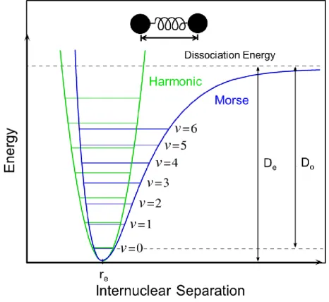
(40) If electrostatic charges are present, we add the appropriate Coulomb potentials:. vCoulomb (r) =. Q1 Q 2 4πϵ0 r. (23). where Q1, Q2 are the charges and ϵ0 is the permittivity of free space. Another common pair potential which is used in our MD simulation is Morse pair potential. Morse potential is also simple and widely used to define interatomic interactions. Morse potential is given by: V(r) = De (𝑒 −2𝑎(𝑟−𝑟𝑒) − 2𝑒 −1(𝑟−𝑟𝑒) ). (24). where r is the distance between the atoms, re is the equilibrium bond distance, De is the well depth (defined relative to the dissociated atoms), and a controls the 'width' of the potential (the smaller a is, the larger the well).. Fig. 19: Morse potential includes the disassociation energy between two atoms. 36.
(41) Chapter 3: High Speed Properties in Modulation Channel Width (MCW) GFET 3.1 Introduction of Chapter 3 As discussed in the first chapter, there is still a dire need to improve the performance of graphene transistor that is being researched and proposed to date since there is no research that has been able to systematically solve the most critical issue of enhancing graphene device's high speed transport property while introducing a bandgap inside the graphene channel at the same time. In this chapter, the first part of the issue is focused, where a new GFET structure is proposed to enhance the high speed property of carriers inside the graphene channel. Monte Carlo device simulation is used to estimate the transport and electrical property of this device. This device is called a Modulated Channel Width Graphene Field Effect Transistor (MCW-GFET). To evaluate the transport properties in MCW-GFET, the mean velocity profile of simulated devices are focused on. From the profile, transit time, τ is extrapolated and evaluated. The highspeed performance enhancement is determined by a faster transit time. Although the newly proposed structure might be complex to be fabricated with any other semiconducting materials, the two-dimensional physics of graphene makes such fabrication possible. Advanced etching technology such as focused He-ion beam milling can be used to fabricate graphene nano device with the capability of sub-10 nm [95].. 3.2 Overshoot velocity effect in short-channel FET It was found that the carrier velocity was higher than its saturation velocity in a short-channel FET where the carrier velocity peaked before saturated [96]. This is called an overshoot velocity effect were the carriers in semiconductors response timedependently to the electric field and if the electric field is high enough, the carrier stay in an overshoot final velocity for a several picoseconds [97]. The overshoot velocity phenomenon occurs due to two reasons [98]. First, when the momentum relaxation rate is larger than the energy relaxation rate. Second, there is a heavier mass conduction valley at low enough energy where the electrons significantly populate at steady state. So, by increasing the electric field along the graphene channel, we can accelerate the carriers in the GFET to achieve a higher overshoot velocity. It is suggested that 37.
(42) overshoot velocity in graphene is due to the first factor where overshoot velocity occurs because of larger momentum relaxation time compared to energy relaxation rate. This carrier acceleration will enhance the high-frequency and high-speed performance, such as a faster transit time, especially when taking place at the source side of the channel [99, 100]. In that case, it is considered that introduction of a high electric field at especially the source side of the channel is crucial in order to shorten the transit time in transistors. There are several methods to do so. Methods such as increasing the doping concentration or changing the thickness of the source and drain regime can introduce this high electric field. However these methods will consequently change the threshold voltage of the transistor.. Fig. 20: Velocity overshoots effect in Silicon. Reprinted with permission from [98]. Copyright by IEEE.. 38.
(43) Fig. 21: Velocity overshoots effect in Graphene FET. Reprinted with permission from [101].. In a previous theoretical study by Awano et al. [102], it was reported that the carrier mean velocity increased significantly (30%) in a HEMT with a nonuniformed channel. It was speculated that this result is due to introduction of a high electric field at the source side of the channel without changing the threshold voltage. This high electric field was yields by the nonuniformed structure of the HEMT.. 39.
(44) Fig. 22: HEMT with nonuniformed channel structure. Average velocity of the transistor in such channel increased.. 3.3 Design Principle of MCW-GFET The new GFET structure introduces a local modulation of the channel width and is called a Modulation Channel Width (MCW) GFET. In this novel structure, the modulation of the width involved locally narrowing the channel width specifically at the source side of the channel. The motivation behind this channel modulation is to achieve a strong electric field at the modulated region that will accelerate the carrier’s velocity inside the channel. This will lead to a higher performance FET in terms of the high speed velocity. The theory is that the strong electric field can be induced at modulation region since there is higher density of electrical flux in that region as a result of the narrowed channel width. This carrier acceleration by the strong electric field will then translate into a faster carrier transit time. It is worth noting that since this channel modulation is done at its width, no change in the threshold voltage can be expected. This is how the overshoot velocity effect is adopted.. 40.
(45) 3.4 Simulation Model of MCW-GFET for High Speed Enhancement 3.4.1 Simulated Device Structure The general structure of the device considered in this simulation is shown in Fig. 23. Insulators are formed on both the top and bottom parts of the graphene channel forming a sandwich device structure. The thickness of both insulators is 10 nm with a dielectric constant of 2.4ε0. The graphene channel is doped n+(1x1018 cm-3) -n(1x1016 cm-3) - n+(1x1018 cm-3). The lengths of the n+-layer source, n+-layer drain, and n-layer channel are all 100 nm in length, making the device dimension 300 nm long. The initial number of particles is 20 000 and the lattice temperature is set to 300 K.. Fig. 23: Modeled device structure. The scattering mechanisms being considered in this simulation are acoustic phonon elastic scattering and inelastic optical phonon emission. The scattering rates for elastic scattering and inelastic phonon emission are 1.0×10¹³ and 1.0×10¹² respectively. It is assumed that the scattering rate is independent of energy, electron density, and. 41.
(46) spatial distribution. Such approximation is considered as it is shown that an average of only 4% difference was found when comparing the velocity profiles in devices with an energy dependent model and the constant model as reported by N. Harada et al. using the same scattering rate value [104]. The optical phonon energy is 0.155 eV. We perform the Monte Carlo motion simulation at the x-axis while solving Poisson’s equation at the x-z plane [103]. In order to achieve the MCW GFET structure, we adjust the width ratio, W of the graphene channel all along the device, creating notches at the source and gate region. W is given by channel dimension (WM the number of stripes) /W0, as shown in Fig. 23.. 3.4.2 Quasi 3D Poisson solver Since this generates a nonuniform channel in the y-direction of the device, the Poisson’s equation is modified to include W as a new parameter in the 2D x-z plane Poisson’s solver, and with that, a quasi-3D Poisson’s equation is achieved.. Fig. 24: Charge confined in a nonuniform cubic 2D Poisson’s equation:. 42.
(47) 𝑈𝑖−1,𝑗 + 𝜁𝑈𝑖,𝑗−1 − 2(1 + 𝜁)𝑈𝑖𝑗 + 𝜁𝑈𝑖,𝑗+1 + 𝑈𝑖+1,𝑗 where 𝜁 =. Δ𝑥 2 𝑁𝑖,𝑗 =− 𝜀. (2 ). 𝛥𝑥 2 𝛥𝑧 2. Quasi-3D Poisson’s equation: 𝑈𝑖−1,𝑗 ∙ m (𝑊𝑖 , 𝑊𝑖−1 ) + 𝜁𝑈𝑖,𝑗−1 ∙ 𝑊𝑖 − [2𝜁𝑊𝑖 + m (𝑊𝑖 , 𝑊𝑖−1 ) + m (𝑊𝑖+1 , 𝑊𝑖 )]𝑈𝑖𝑗 Δ𝑥 2 𝑁𝑖,𝑗 + 𝜁𝑈𝑖,𝑗+1 ∙ 𝑊𝑖 + 𝑈𝑖+1,𝑗 ∙ m (𝑊𝑖+1 , 𝑊𝑖 ) = − 𝜀. (2 ). This quasi-3D Poisson’s equation is derived using Gauss’s Law by considering a situation wherein an electric charge is confined in a nonuniformly shaped cubic as shown in Fig.20. The total charge over 𝜀, enclosed within the cubic can be defined by:. 𝜀. =∯. 𝑑. (28). The surface integral of electric field then can be defined using the given component EA, EB, ECand EDas:. ∯. 𝑑 = 𝐸 ∙ Δ𝑥 ∙ 𝑊𝑖 + 𝐸𝐵 ∙ Δ𝑧 ∙ m (𝑊𝑖, 𝑊𝑖−1 ) + 𝐸𝐶 ∙ Δ𝑥 ∙ 𝑊𝑖. +𝐸𝐷 ∙ Δ𝑧 ∙ m (𝑊𝑖+1, 𝑊𝑖 ). (29). Since, 𝑈𝑖,𝑗−1 − 𝑈𝑖𝑗 ) ∆𝑧 𝑈𝑖−1,𝑗 − 𝑈𝑖𝑗 𝐸𝐵 = (− ) ∆𝑥 𝑈𝑖,𝑗+1 − 𝑈𝑖𝑗 𝐸𝐶 = (− ) ∆𝑧 𝐸 = (−. 43. (30) (31) (32).
(48) 𝐸𝐷 = (−. 𝑈𝑖+1,𝑗 − 𝑈𝑖𝑗 ) ∆𝑥. (33). Equation (29) can be expanded to: 𝑈𝑖,𝑗−1 − 𝑈𝑖𝑗 𝑈𝑖−1,𝑗 − 𝑈𝑖𝑗 ( ) ∙ Δ𝑥 ∙ 𝑊𝑖 + ( ) ∙ Δ𝑧 ∙ m (𝑊𝑖, 𝑊𝑖−1 ) + ∆𝑧 ∆𝑥 𝑈𝑖,𝑗+1 − 𝑈𝑖𝑗 𝑈𝑖+1,𝑗 − 𝑈𝑖𝑗 ( ) ∙ Δ𝑥 ∙ 𝑊𝑖 + ( ) ∙ Δ𝑧 ∙ m (𝑊𝑖+1, 𝑊𝑖 ) = ∆𝑧 ∆𝑥 𝜀 Δ𝑥 Δ𝑧 ∙ 𝑊𝑖 (𝑈𝑖,𝑗−1 − 2𝑈𝑖𝑗 + 𝑈𝑖,𝑗+1 ) + [(𝑈𝑖−1,𝑗 − 𝑈𝑖𝑗 ) ∙ m (𝑊𝑖, 𝑊𝑖−1 ) Δ𝑧 ∆𝑥 +(𝑈𝑖+1,𝑗 − 𝑈𝑖𝑗 ) ∙ m (𝑊𝑖+1, 𝑊𝑖 )] =. By replacing. 𝜀. (34). = ∆𝑥∆𝑧𝑊𝑖 ∙ 𝑞 ∙ 𝑁𝑖𝑗 which represents electric charge in device, (𝑞 is the. charge per electron and 𝑁𝑖𝑗 is the carrier density) 𝑈𝑖−1,𝑗 ∙ m (𝑊𝑖 , 𝑊𝑖−1 ) + + m (𝑊𝑖+1 , 𝑊𝑖 )]𝑈𝑖𝑗 +. By replacing 𝜁. =. 𝛥𝑥 2 𝛥𝑧 2. 𝛥𝑥 2 𝛥𝑥 2 𝑈 ∙ 𝑊 − [2 𝑊 + m (𝑊𝑖 , 𝑊𝑖−1 ) 𝑖 𝛥𝑧 2 𝑖,𝑗−1 𝛥𝑧 2 𝑖. Δ𝑥 2 𝑁𝑖,𝑗 𝛥𝑥 2 (𝑊 ) 𝑈 ∙ 𝑊 + 𝑈 ∙ m , 𝑊 = − 𝑖 𝑖+1,𝑗 𝑖+1 𝑖 𝛥𝑧 2 𝑖,𝑗+1 𝜀. (35). , equation (27) is derived.. The value of W is adjusted along the devices such that it defines the narrowed or modulated channel region.. 44.
(49) 3.5 Result and Discussion 3.5.1 Electric Field Profile (MCW-GFET W= 0.1, W= 0.3) Performance estimation is started by evaluating the electric field profile specifically at the modulation region near the source side of the channel (Position, X= 100-150 nm). From the result shown in Fig. 25 and Fig. 26, we find out that strong electric field are induced in both MCW-GFET devices with a monolayer and a bilayer channel. The strongest electric field is up to 2×10⁴ and 1.68×10⁴ V/cm in monolayer and bilayer MCW-GFET devices respectively when W=0.1 in both cases. This result shows that introduction of local strong electric field is achieved at the modulated region as can be seen when observing the electric field inside the whole channel of the device in Fig. 27.. 45.
(50) Fig. 25: Electric Field in MCW-GFET with a bilayer graphene channel. 46.
(51) Fig. 26: Electric Field in MCW-GFET with a monolayer graphene channel. 47.
(52) Fig. 27: Full Electric Field profile in MCW-GFET and Conventional GFET with a monolayer graphene channel. Local stronger electric filed is introduced at the modulated region.. 48.
(53) 3.5.2 Mean Carrier Velocity (MCW-GFET W= 0.1, W= 0.3) Next, we further observed the mean carrier velocity in both devices to see the effect of stronger electric field. It was evident from the results in both MCW-GFETs with bilayer and monolayer graphene channel that stronger electric fields had an effect on mean carrier velocity shown in Fig. 28 and Fig. 29. The mean carrier velocity increased in both cases when W=0.3 and W= 0.1. When clearly observed, in the case of device with bilayer graphene channel, the highest increase in the mean velocity (W= 0.1) was observed near the source region, 22nm from the source edge inside the channel region. It is a 52% increase from 1.67×10⁵ to 3.93×10⁵ m/s. When taking the transit time τ of the particles into account, the time needed for the carriers to travel along the channel from the source to the drain region of the MCWGFET, it shortened greatly by 38% from 0.38 to 0.24 ps. Since the intrinsic highfrequency high-velocity performance is frequently determined by looking at the transit time near source region in the n channel, the transit time at a particular region (X = 80 to 130 nm), where the notches are introduced are also observed. This modulated region transit time is denoted as τ*. Surprisingly, the MCW-GFET showed τ*of 0.23 ps, while the conventional GFET possessed τ*of 0.5 ps, which simply indicates that the modulated region transit time had shortened by 54%, more than half in the MCWGFET. The device with W= 0.3, on the other hand, showed a similar increase in velocity of up to 42% near the source region. The local mean velocity increased from 1.67×10⁵ to 2.86×10⁵ m/s. In such device, τ*shortened by 36% from 0.5 to 0.32 ps. On the other hand, in the case of monolayer graphene, the maximum increase in the mean velocity (W=0.1) was observed 8 nm from the source edge inside the channel region where X = 92 nm. The mean velocity increases up to 64%, from 8.58×10⁴ to 2.39×10⁵ m/s. The transit time is however only shortened by 13% from 0.15 to 0.13ps. τ*on the other hand shortened by 30% from 0.14 to 0.1 ps. Device with W= 0.3 showed 8% faster transit time and 9% faster modulated region transit time.. 49.
(54) Fig. 28: Mean carrier velocity in MCW-GFET with bilayer graphene channel. Modulated region transit time, τ* is the transit time at the source side of the channel.. 50.
(55) Fig. 29: Mean carrier velocity in MCW-GFET with monolayer graphene channel. Modulated region transit time, τ* is the transit time at the source side of the channel.. 51.
(56) 3.5.3 MCW Effect in Monolayer and Bilayer Graphene Channel It has been shown that the MCW structure introduce a sharp electric field increase at the source side at the channel and the enhancement of the high speed property which is translate as a faster transit time inside both monolayer and bilayer graphene channel. Although faster transit time can be found in both MCW-GFET with monolayer and bilayer graphene channel, it can be seen from the results that the MCW effect is more significant in MCW-GFET with a bilayer graphene channel. Although the mechanism of the MCW effect will later be discussed in chapter 4, here the why there is a more significant enhancement in terms of carrier velocity of MCW-GFET with a bilayer channel over of a monolayer graphene channel is discussed. It is suggested that this different effect of the MCW structure correlates with the nature of the bandstructure inside bilayer and monolayer graphene. It is clear that stronger electric field shift the carrier distribution to higher energy region, which is shown in carrier mean energy profile of Fig. 30 and Fig. 31. In the region where the notches were placed (X= 100-150 nm), the energy significantly increased in MCWGFETs. The highest increased was at X= 132 nm where the mean energy doubled from 0.0273 to 0.0576 eV. The nature of the E-k dispersion in bilayer graphene is parabolic while is linear in monolayer graphene such that the maximum velocity calculated from the slope of the dispersion does not change in monolayer graphene even in higher energy regions. This maximum velocity does change in bilayer graphene because of the parabolic dipersion. Therefore, shift of the carrier distribution to higher energy region is more significant in contributing to the velocity enhancement in the case of bilayer graphene channel.. 52.
(57) Fig. 30: Energy profile in MCW-GFET with bilayer graphene channel. 53.
(58) Fig. 31: Energy profile in MCW-GFET with monolayer graphene channel. 54.
(59) 3.6 Conclusion of Chapter 3 In conclusion, the feasibility of a new MCW-GFET with its channel width being locally modulated is being demonstrated. With dimension optimization, a 54% faster modulated region transit time was achieved in such device. It has been found that local modulation of the channel width introduces a high acceleration electric field near the notch structure but will not change the threshold voltage Vth of the FET. The nature of the parabolic band dispersion in bilayer graphene makes the MCW effect more significant is such compared to a monolayer graphene. These findings open a new dimension for fabricating high-speed high-frequency transistors with structural design.. 55.
(60) Chapter 4: Bandgap Opening in Modulated Channel Width (MCW) GFET 4.1 Introduction of Chapter 4 It was demonstrated in the previous chapter that such local modulation of the channel width at the source side of the channel enhanced the high frequency& highspeed performance with almost no changing the threshold voltage of the transistor. In this chapter, the MCW structure is extended to not only enhance the high speed property of carriers but to open a bandgap inside the graphene channel. The electrical and transport properties of MCW-GFET, where a GNR array is created at the modulation area as shown in Fig. 32 is explored. The feasibility of this structure in terms of high speed carrier transport and bandgap creation in the channel is investigated for the first time, by using a semi classical Monte Carlo particle method for simulating electron transport combined with an ab-initio method for calculating band structures of GNR. The bandstructure of GNR array structure is evaluate focusing on two important values which are the bandgap and the slope of the energy dispersion. These two values are crucial to determine the performance of the device in terms of the high-speed performance which is influenced by the slope and switching characteristic which is determined by the value of the bandgap.. Fig. 32: GNR array introduced in the modulated region of the graphene channel. 56.
(61) 4.2 Graphene Nanoribbon (GNR) It has been known that quantum confinement in thin graphene ribbon or more well-known as graphene nanoribbon (GNR) creates a bandgap in graphene channel [104, 105]. The bandgap opening can be controlled by tuning the width and edge state of the GNR [106, 107]. The edge state of the GNR in particular is very sensitive to the bandgap opening. An armchair or a zig-zag edge is reported to sensitively determine whether the GNR will be semiconducting or metallic [108, 109, 110]. In addition, the nature of the bandgap is reported to be inversely proportional with the GNR width [28]. To yield a significant bandgap of >100 meV, a GNR with a width of <10 nm should be considered. The problem with GNR device as a solution to a GFET with no bandgap is the fact that GNR-FET exhibits a low carrier velocity and a low driving current as discuss briefly earlier in the first chapter.. 4.3 Bandgap Calculation (10 nm GNR, Bilayer Graphene) Since calculation is performed while considering periodicity in Y-direction, the band structure of GNR stripes is assumed to be similar to a single stripe of 10 nm-wide nanoribbon calculated using the unit cell in Fig. 33. The GNR arm-chair edges are terminated by hydrogen atoms while Fig. 34 shows the structure of bilayer graphene channel that is also being calculated with a perpendicular electric field applied in order to open a bandgap. The geometry in both cases of GNR and Bilayer Graphene is optimized until the force tolerance is 0.01 meV/A. The Monkhorst-Pack grid k point sampling is set to be 1×16×16 in GNR and 11×11×1 in Bilayer Graphene. The most general exchange correlation, Local Density Approximation (LDA) is used in this calculation. The bandstructures of both GNR and bilayer graphene with a perpendicular electric field are shown in Fig. 35 and Fig. 36 respectively. A 100 meV bandgap openings is obtained in the GNR structure and this agree well previous works [111]. In order to compare the performance of devices with the same bandgap opening, the perpendicularly applied electric field of bilayer graphene channel is controlled and tuned to achieve a 100 meV bandgap. It is found that a 1.2 V/nm electric field yield a 100 nm in such case and agree considerably well with past literature [112].. 57.
(62) Fig. 33: Unit cell of GNR. Fig. 34: Unit cell of Bilayer Graphene with a perpendicular electric field being applied. 58.
(63) Fig. 35: Bandstructure of a 10 nm GNR. Fig. 36: Bandstructure of a Bilayer Graphene with a 1.2 V/nm electric field being applied perpendicularly. 59.
Gambar
![Fig. 3: ITRS roadmap for the current density of Copper (Cu) [15] Reprinted and modified with permission from ITRS 2013 Edition, Interconnect, Figure INTC9](https://thumb-ap.123doks.com/thumbv2/123dok/1874823.2665114/11.892.238.655.551.904/roadmap-current-density-reprinted-modified-permission-edition-interconnect.webp)
![Fig. 4: Increasing resistivity of Cu interconnect with width of <100nm [16]](https://thumb-ap.123doks.com/thumbv2/123dok/1874823.2665114/12.892.244.658.154.510/fig-increasing-resistivity-cu-interconnect-width-lt-nm.webp)
![Fig. 6: Graphene structure as a unit that can formed fullerene and CNT. This is modified from[25]](https://thumb-ap.123doks.com/thumbv2/123dok/1874823.2665114/15.892.286.651.631.1044/fig-graphene-structure-unit-formed-fullerene-cnt-modified.webp)
+7
![Fig. 20: Velocity overshoots effect in Silicon. Reprinted with permission from [98].](https://thumb-ap.123doks.com/thumbv2/123dok/1874823.2665114/42.892.134.730.496.982/fig-velocity-overshoots-effect-silicon-reprinted-permission.webp)
![Fig. 21: Velocity overshoots effect in Graphene FET. Reprinted with permission from [101]](https://thumb-ap.123doks.com/thumbv2/123dok/1874823.2665114/43.892.221.682.154.621/fig-velocity-overshoots-effect-graphene-fet-reprinted-permission.webp)
Dokumen terkait
Perbedaan Radar dengan system komunikasi umumnya terletak pada level margin penerima, Kekuatan pantulan sinyal yang diterima oleh radar bervariasi tergantung dari jarak
Pelaksanaan pendidikan agama Islam melalui metode bercerita di Taman Kanak- kanak Hidayatut Thalibin Cilanclak dilakukan dengan cara menyajikan cerita- cerita yang
Bersama ini kami menyatakan LELANG GAGAL sesuai dengan ketentuan peraturan yang berlaku. Demikian Pengumuman ini disampaikan
Sebab materi ajar pada Buku Pegangan Belajar Siswa dan LKS (yang dijual bebas) belum tentu sesuai dengan rencana pembelajaran yang disusun oleh guru.. Karena RPP disusun sendiri
PLTMH umumnya merupakan pembangkit listrik jenis run of river dimana head diperoleh dengan cara mengalihkan aliran air sungai ke satu sisi dari sungai tersebut selanjutnya
Dian Mey Saputri A210090172, Program Studi Pendidikan Akuntansi, Fakultas Keguruan dan Ilmu Pendidikan, Universitas Muhammadiyah Surakarta, 2013. Tujuan penelitian ini
PENGEMBANGAN MODUL PEMBELAJARAN GEOGRAFI BERBASIS PEDULI LINGKUNGAN PADA MATERI SUMBER DAYA ALAM.. DI KELAS XI IPS SMA BINA
Mira Adita Widianti, D0212070, KOMUNIKASI INTERPERSONAL MEMBANGUN KEPERCAYAAN KOMUNITAS NEBENGERS MELALUI MEDIA SOSIAL (Studi Kasus Proses Komunikasi Interpersonal dalam
