44
Lampiran 1
45
Lampiran 2
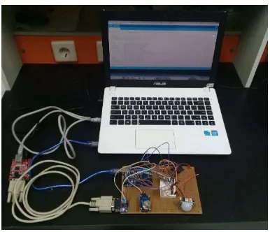
Program Arduino Uno
#include <EEPROM.h>
#include <DHT.h>
//Constants
#define DHTPIN 4
#define DHTTYPE DHT22
//DHT dht(DHTPIN, DHTTYPE);
//Variables
int LDR= A2;
int pirPin = 6;
int redLED= 13;
int greenLED=12;
int nilaiLDR= 0;
int buzzerPin = 11;
int pirState = LOW;
float hum;
float temp;
int MQ2 = A3;
int MQ2Value = 0;
int address = 0;
int startAddress = 60;
void setup() {
Serial.begin(9600);
Serial.println("DHT22 Temperature dan Humidity ke EEPROM");
Serial.print("Data dimulai pada lokasi EEPROM ");
46
pinMode(pirPin, INPUT);
pinMode (MQ2, INPUT);
dht.begin();
}
void loop()
{
//SENSOR TEMPERATUR DAN KELEMBABAN (DHT22)
//hum = dht.readHumidity();
//temp= dht.readTemperature();
Serial.print("Humidity: ");
Serial.print(hum);
Serial.print(" RH, Temp: ");
Serial.print(temp);
Serial.println("C");
if (temp >= 32){
tone(buzzerPin, 956, 200);
delay (500);
tone(buzzerPin, 956, 200);
delay (500);
tone(buzzerPin, 956, 200);
delay (500);
tone(buzzerPin, 956, 200);
delay (500);
tone(buzzerPin, 956, 200);
delay (500);
Serial.println ("OVER HEAT"); }
else if (temp <= 28){
digitalWrite (greenLED, HIGH);
Serial.println ("LOW TEMPERATURE");}
else if (temp = 29, temp = 31){
digitalWrite (greenLED, LOW);
47
// SENSOR PERGERAKAN (PASSIVE INFRARED)
Val = digitalRead (pirPin);
if(Val == HIGH) {
if (pirState == LOW) {
Serial.println("Motion Detected");
pirState = HIGH;
tone(buzzerPin, 956, 200);
delay (500);
tone(buzzerPin, 956, 200);
delay (500);
tone(buzzerPin, 956, 200);
delay (500);
tone(buzzerPin, 956, 200);
delay (500);
tone(buzzerPin, 956, 200);
delay (500);
} }
else {
if (pirState == HIGH){
noTone(buzzerPin);
Serial.println("Motion Ended");
pirState = LOW; }}
delay (2000);
//SENSOR CAHAYA (LDR)
{
48
digitalWrite(redLED, LOW);
delay (2000);
}}
// Sensor Asap dan Gas
{
MQ2Value = analogRead (MQ2);
Serial.print ("NilaiMQ2= ");
Serial.println (MQ2Value);
if (MQ2Value >= 300 ) {
tone(buzzerPin, 956, 200);
delay (500);
tone(buzzerPin, 956, 200);
delay (500);
tone(buzzerPin, 956, 200);
delay (500);
tone(buzzerPin, 956, 200);
delay (500);
tone(buzzerPin, 956, 200);
delay (500);
Serial.println ("Status Asap : YES ");
} else
Serial.println ("Status Asap : NO"); noTone(buzzerPin);
delay (2000); // delay 2 sec
49
Lampiran 3
Aosong Electronics Co.,Ltd
Your specialist in innovating humidity & temperature sensors
Digital-output relative humidity & temperature sensor/module
DHT22 (DHT22 also named as AM2302)
Capacitive-type humidity and temperature module/sensor
Aosong Electronics Co.,Ltd
Your specialist in innovating humidity & temperature sensors
1. Feature & Application:
* Full range temperature compensated * Relative humidity and temperature measurement
* Calibrated digital signal *Outstanding long-term stability *Extra components not needed
* Long transmission distance * Low power consumption *4 pins packaged and fully interchangeable
2. Description:
DHT22 output calibrated digital signal. It utilizes exclusive digital-signal-collecting-technique and humidity
sensing technology, assuring its reliability and stability.Its sensing elements is connected with 8-bit single-chip
computer.
Every sensor of this model is temperature compensated and calibrated in accurate calibration chamber and the
calibration-coefficient is saved in type of programme in OTP memory, when the sensor is detecting, it will cite
coefficient from memory.
Small size & low consumption & long transmission distance(20m) enable DHT22 to be suited in all kinds of
harsh application occasions.
Single-row packaged with four pins, making the connection very convenient.
3. Technical Specification:
Model
DHT22
Power supply
3.3-6V DC
Output signal
digital signal via single-bus
Sensing element
Polymer capacitor
Operating range
humidity 0-100%RH; temperature -40~80Celsius
Accuracy
humidity +-2%RH(Max +-5%RH); temperature <+-0.5Celsius
Resolution or sensitivity
humidity 0.1%RH; temperature 0.1Celsius
Repeatability
humidity +-1%RH; temperature +-0.2Celsius
Humidity hysteresis
+-0.3%RH
Long-term Stability
+-0.5%RH/year
Sensing period
Average: 2s
Interchangeability
fully interchangeable
Dimensions
small size 14*18*5.5mm; big size 22*28*5mm
4. Dimensions: (unit----mm)
Aosong Electronics Co.,Ltd
Your specialist in innovating humidity & temperature sensors
Aosong Electronics Co.,Ltd
Your specialist in innovating humidity & temperature sensors
Pin sequence number: 1 2 3 4 (from left to right direction).
Pin
Function
1
VDD----power supply
2
DATA--signal
3
NULL
Aosong Electronics Co.,Ltd
Your specialist in innovating humidity & temperature sensors
5. Electrical connection diagram:
3Pin---NC, AM2302
is another name for DHT22
6. Operating specifications:
(1) Power and Pins
Power's voltage should be 3.3-6V DC. When power is supplied to sensor, don't send any instruction to the sensor
within one second to pass unstable status. One capacitor valued 100nF can be added between VDD and GND for
wave filtering.
(2) Communication and signal
Single-bus data is used for communication between MCU and DHT22, it costs 5mS for single time
communication.
Data is comprised of integral and decimal part, the following is the formula for data.
DHT22 send out higher data bit firstly!
DATA=8 bit integral RH data+8 bit decimal RH data+8 bit integral T data+8 bit decimal T data+8 bit check-sum
If the data transmission is right, check-sum should be the last 8 bit of "8 bit integral RH data+8 bit decimal RH
data+8 bit integral T data+8 bit decimal T data".
When MCU send start signal, DHT22 change from low-power-consumption-mode to running-mode. When MCU
finishs sending the start signal, DHT22 will send response signal of 40-bit data that reflect the relative humidity
Aosong Electronics Co.,Ltd
Your specialist in innovating humidity & temperature sensors
and temperature information to MCU. Without start signal from MCU, DHT22 will not give response signal to
MCU. One start signal for one time's response data that reflect the relative humidity and temperature information
from DHT22. DHT22 will change to low-power-consumption-mode when data collecting finish if it don't receive
start signal from MCU again.
1) Check bellow picture for overall communication process:
Host computer send out
start signal. Data transmission finished,
Sensor send out and RL pull up bus's voltage
response signal. Output data: 1bit"0" for next transmission
Pull up and wait Host's signal Sensor's signal Output data: 1bit "1"
response from sensor Sensor pull down
Pull up voltage and get bus's voltage
ready for sensor's output.
Single-bus output
---2) Step 1: MCU send out start signal to DHT22
Data-bus's free status is high voltage level. When communication between MCU and DHT22 begin, program of
MCU will transform data-bus's voltage level from high to low level and this process must beyond at least 1ms to
ensure DHT22 could detect MCU's signal, then MCU will wait 20-40us for DHT22's response.
Aosong Electronics Co.,Ltd
Your specialist in innovating humidity & temperature sensors
Host computer send start signal Sensor send out response signal
and keep this signal at least
1ms
and keep this signal 80us
Host pull up voltage
-and wait sensor's response Sensor pull up bus's voltage
Signal from host Start data transmission
Signal from sensor
Single-bus signal
Step 2: DHT22 send response signal to MCU
When DHT22 detect the start signal, DHT22 will send out low-voltage-level signal and this signal last 80us as
response signal, then program of DHT22 transform data-bus's voltage level from low to high level and last 80us
for DHT22's preparation to send data.
Check bellow picture for step 2:
Aosong Electronics Co.,Ltd
Your specialist in innovating humidity & temperature sensors
Start transmit 1bit data Start transmit next bit data
26-28us voltage-length means data "0"
Host signal Sesnor's signal
Single-bus signal
Step 3: DHT22 send data to MCU
When DHT22 is sending data to MCU, every bit's transmission begin with low-voltage-level that last 50us, the
following high-voltage-level signal's length decide the bit is "1" or "0".
Aosong Electronics Co.,Ltd
Your specialist in innovating humidity & temperature sensors
70us voltage-length means 1bit data "1"
Start transmit 1bit data Start transmit next bit data
Host signal Sesnor's signal
Single-bus signal
If signal from DHT22 is always high-voltage-level, it means DHT22 is not working properly, please check the
electrical connection status.
7. Electrical Characteristics:
Item
Condition
Min
Typical
Max
Unit
Power supply
DC
3.3
5
6
V
Current supply
Measuring
1
1.5
mA
Stand-by
40
Null
50
uA
Collecting
period
Second
2
Second
*Collecting period should be : >2 second.
Aosong Electronics Co.,Ltd
Your specialist in innovating humidity & temperature sensors
8. Attentions of application:
(1) Operating and storage conditions
We don't recommend the applying RH-range beyond the range stated in this specification. The DHT22 sensor
can recover after working in non-normal operating condition to calibrated status, but will accelerate sensors'
aging.
(2) Attentions to chemical materials
Vapor from chemical materials may interfere DHT22's sensitive-elements and debase DHT22's sensitivity.
(3) Disposal when (1) & (2) happens
Step one: Keep the DHT22 sensor at condition of Temperature 50~60Celsius, humidity <10%RH for 2 hours;
Step two: After step one, keep the DHT22 sensor at condition of Temperature 20~30Celsius, humidity
>70%RH for 5 hours.
(4) Attention to temperature's affection
Relative humidity strongly depend on temperature, that is why we use temperature compensation technology to
ensure accurate measurement of RH. But it's still be much better to keep the sensor at same temperature when
sensing.
DHT22 should be mounted at the place as far as possible from parts that may cause change to temperature.
(5) Attentions to light
Long time exposure to strong light and ultraviolet may debase DHT22's performance.
(6) Attentions to connection wires
The connection wires' quality will effect communication's quality and distance, high quality shielding-wire is
recommended.
(7) Other attentions
* Welding temperature should be bellow 260Celsius.
* Avoid using the sensor under dew condition.
* Don't use this product in safety or emergency stop devices or any other occasion that failure of DHT22 may
cause personal injury.
Email: [email protected] or [email protected]
Visit us at http://www.sunrom.com
Document: Datasheet Date: 28-Jul-08 Model #: 3190 Product’s Page: www.sunrom.com/p-510.html
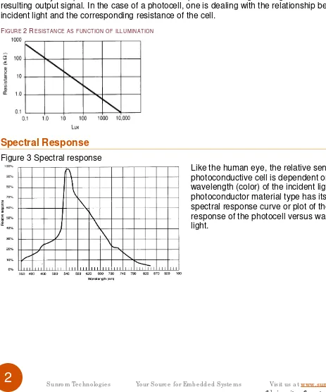
Light Dependent Resistor - LDR
Two cadmium sulphide(cds) photoconductive cells with spectral responses
similar to that of the human eye. The cell resistance falls with increasing light
intensity. Applications include smoke detection, automatic lighting control,
batch counting and burglar alarm systems.
Applications
Photoconductive cells are used in many different types of circuits and
applications.
Analog Applications
•
Camera Exposure Control
•
Auto Slide Focus - dual cell
•
Photocopy Machines - density of toner
•
Colorimetric Test Equipment
•
Densitometer
•
Electronic Scales - dual cell
•
Automatic Gain Control – modulated light
source
•
Automated Rear View Mirror
Digital Applications
•
Automatic Headlight Dimmer
•
Night Light Control
•
Oil Burner Flame Out
•
Street Light Control
•
Absence / Presence (beam breaker)
•
Position Sensor
Electrical Characteristics
Parameter
Conditions
Min
Typ
Max
Unit
Cell resistance
1000 LUX
10 LUX
Power Dissipation
100
mW max
Operating
Temperature
Guide to source illuminations
Light source Illumination
LUX
Moonlight
0.1
60W Bulb at 1m
50
1W MES Bulb at 0.1m
100
Fluorescent Lighting
500
Bright Sunlight
30,000
Sensitivity
The sensitivity of a photodetector is the relationship between the light falling on the device and the
resulting output signal. In the case of a photocell, one is dealing with the relationship between the
incident light and the corresponding resistance of the cell.
FIGUR E 2RESIST ANCE AS FUNCT ION OF ILLU MINAT ION
Spectral Response
Figure 3 Spectral response
Like the human eye, the relative sensitivity of a
photoconductive cell is dependent on the
wavelength (color) of the incident light. Each
photoconductor material type has its own unique
spectral response curve or plot of the relative
response of the photocell versus wavelength of
light.
FIGUR E 1CIRCUITSYMBOL
R1
Dimensions
5V
Buy TechnicalDocuments Tools &Software
Support & Community
MAX232, MAX232I
SLLS047M – FEBRUARY 1989 – REVISED NOVEMBER 2014
MAX232x Dual EIA-232 Drivers/Receivers
1 Features
3 Description
The MAX232 device is a dual driver/receiver that
1•
Meets or Exceeds TIA/EIA-232-F and ITU
includes a capacitive voltage generator to supply
Recommendation V.28
TIA/EIA-232-F voltage levels from a single 5-V
•
Operates From a Single 5-V Power Supply With
supply. Each receiver converts TIA/EIA-232-F inputs
1.0-µF Charge-Pump Capacitors
to 5-V TTL/CMOS levels. These receivers have a
typical threshold of 1.3 V, a typical hysteresis of 0.5
•
Operates up to 120 kbit/s
V, and can accept ±30-V inputs. Each driver converts
•
Two Drivers and Two Receivers
TTL/CMOS input levels into TIA/EIA-232-F levels.
•
±30-V Input Levels
•
Low Supply Current: 8 mA Typical
Device Information
(1)ORDER NUMBER PACKAGE (PIN) BODY SIZE
•
ESD Protection Exceeds JESD 22
SOIC (16) 9.90 mm × 3.91 mm
– 2000-V Human-Body Model (A114-A)
SOIC (16) 10.30 mm × 7.50 mm
•
Upgrade With Improved ESD (15-kV HBM) and
MAX232xPDIP (16) 19.30 mm × 6.35 mm
0.1-µF Charge-Pump Capacitors is Available With
SOP (16) 10.3 mm × 5.30 mm
the MAX202 Device
(1) For all available packages, see the orderable addendum at the end of the datasheet.
MAX232, MAX232I
SLLS047M – FEBRUARY 1989 – REVISED NOVEMBER 2014 www.ti.com
Table of Contents
9.1 Overview ...9
1 Features...1
9.2 Functional Block Diagram ...9
2 Applications...1
9.3 Feature Description...9
3 Description...1
9.4 Device Functional Modes...9
4 Simplified Schematic...1
10 Application and Implementation...10
5 Revision History...2
10.1 Application Information...10
6 Pin Configuration and Functions...3
10.2 Typical Application ...10
7 Specifications...4
11 Power Supply Recommendations...11 7.1 Absolute Maximum Ratings ...4
12 Layout...11 7.2 Handling Ratings...4
12.1 Layout Guidelines ...11
7.3 Recommended Operating Conditions ...4
12.2 Layout Example ...11
7.4 Thermal Information ...4
13 Device and Documentation Support...12 7.5 Electrical Characteristics –– Device ...4
13.1 Related Links ...12
7.6 Electrical Characteristics –– Driver ...5
13.2 Trademarks ...12
7.7 Electrical Characteristics –– Receiver ...5
13.3 Electrostatic Discharge Caution ...12
7.8 Switching Characteristics ...5
13.4 Glossary ...12
7.9 Typical Characteristics ...6
14 Mechanical, Packaging, and Orderable 8 Parameter Measurement Information...7
Information...12
9 Detailed Description...9
5 Revision History
Changes from Revision L (March 2004) to Revision M Page
• Removed Ordering Information table. ... 1 • Added Handling Rating table, Feature Description section, Device Functional Modes, Application and
Implementation section, Power Supply Recommendations section, Layout section, Device and Documentation
1
www.ti.com SLLS047M – FEBRUARY 1989 – REVISED NOVEMBER 2014
6 Pin Configuration and Functions
Top View
Pin Functions
PIN
TYPE DESCRIPTION
NAME NO.
C1+ 1 — Positive lead of C1 capacitor
VS+ 2 O Positive charge pump output for storage capacitor only
C1- 3 — Negative lead of C1 capacitor
C2+ 4 — Positive lead of C2 capacitor
C2- 5 — Negative lead of C2 capacitor
VS- 6 O Negative charge pump output for storage capacitor only T2OUT, T1OUT 7, 14 O RS232 line data output (to remote RS232 system) R2IN, R1IN 8, 13 I RS232 line data input (from remote RS232 system) R2OUT, R1OUT 9, 12 O Logic data output (to UART)
T2IN, T1IN 10, 11 I Logic data input (from UART)
GND 15 — Ground
MAX232, MAX232I
SLLS047M – FEBRUARY 1989 – REVISED NOVEMBER 2014 www.ti.com
7 Specifications
7.1 Absolute Maximum Ratings
(1)over operating free-air temperature range (unless otherwise noted)
MIN MAX UNIT
VCC Input Supply voltage range(2) –0.3 6 V
VS+ Positive output supply voltage range VCC– 0.3 15 V
VS– Negative output supply voltage range –0.3 –15 V
T1IN, T2IN –0.3 VCC+ 0.3
VI Input voltage range V
R1IN, R2IN ±30
T1OUT, T2OUT VS–– 0.3 VS++ 0.3
VO Output voltage range V
R1OUT, R2OUT –0.3 VCC+ 0.3
Short-circuit duration T1OUT, T2OUT Unlimited
TJ Operating virtual junction temperature 150 °C
(1) Stresses beyond those listed underAbsolute Maximum Ratingsmay cause permanent damage to the device. These are stress ratings only, and functional operation of the device at these or any other conditions beyond those indicated underRecommended Operating Conditionsis not implied. Exposure to absolute-maximum-rated conditions for extended periods may affect device reliability. (2) All voltages are with respect to network GND.
7.2 Handling Ratings
MIN MAX UNIT
Tstg Storage temperature range -65 150 °C
Human body model (HBM), per ANSI/ESDA/JEDEC JS-001, all 0 2000 pins(1)
V(ESD) Electrostatic discharge V
Charged device model (CDM), per JEDEC specification 0 1000 JESD22-C101, all pins(2)
(1) JEDEC document JEP155 states that 500-V HBM allows safe manufacturing with a standard ESD control process. (2) JEDEC document JEP157 states that 250-V CDM allows safe manufacturing with a standard ESD control process.
7.3 Recommended Operating Conditions
MIN NOM MAX UNIT
VCC Supply voltage 4.5 5 5.5 V
VIH High-level input voltage (T1IN,T2IN) 2 V
VIL Low-level input voltage (T1IN, T2IN) 0.8 V
R1IN,
Receiver input voltage ±30 V
R2IN
MAX232 0 70
TA Operating free-air temperature °C
MAX232I –40 85
7.4 Thermal Information
MAX232xD MAX232xDW MAX232xN MAX232xNS
THERMAL METRIC(1) SOIC SOIC wide PDIP SOP UNIT
16 PINS 16 PINS 16 PINS 16 PINS
RθJA Junction-to-ambient thermal resistance 73 57 67 64 °C/W
MAX232, MAX232I
www.ti.com SLLS047M – FEBRUARY 1989 – REVISED NOVEMBER 2014
7.6 Electrical Characteristics –– Driver
over recommended ranges of supply voltage and operating free-air temperature (unless otherwise noted)
PARAMETER TEST CONDITIONS(1) MIN TYP(2) MAX UNIT
VOH High-level output voltage T1OUT, T2OUT RL= 3 kΩto GND 5 7 V
VOL Low-level output voltage(3) T1OUT, T2OUT RL= 3 kΩto GND –7 –5 V
rO Output resistance T1OUT, T2OUT VS+= VS–= 0, VO= ±2 V 300 Ω
IOS(4) Short-circuit output current T1OUT, T2OUT VCC= 5.5 V, VO= 0 V ±10 mA
IIS Short-circuit input current T1IN, T2IN VI= 0 200 µA
(1) Test conditions are C1–C4 = 1μF at VCC= 5 V ± 0.5 V (2) All typical values are at VCC= 5 V, TA= 25°C.
(3) The algebraic convention, in which the least-positive (most negative) value is designated minimum, is used in this data sheet for logic voltage levels only.
(4) Not more than one output should be shorted at a time.
7.7 Electrical Characteristics –– Receiver
over recommended ranges of supply voltage and operating free-air temperature (unless otherwise noted)
PARAMETER TEST CONDITIONS(1) MIN TYP(2) MAX UNIT
VOH High-level output voltage R1OUT, R2OUT IOH= –1 mA 3.5 V
VOL Low-level output voltage(3) R1OUT, R2OUT IOL= 3.2 mA 0.4 V
Receiver positive-going input threshold
(3) The algebraic convention, in which the least-positive (most negative) value is designated minimum, is used in this data sheet for logic voltage levels only.
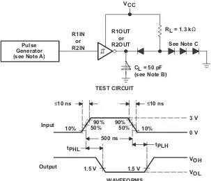
7.8 Switching Characteristics
over recommended ranges of supply voltage and operating free-air temperature (unless otherwise noted)
PARAMETER TEST CONDITIONS(1) MIN TYP(1) MAX UNIT
SR Driver slew rate RL = 3 kΩto 7 kΩ, seeFigure 4 30 V/μs
SR(t) Driver transition region slew rate seeFigure 5 3 V/μs
Data rate One TOUT switching 120 kbit/s
Receiver propagation delay time,
tPLH®) low- to high-level output TTL load, seeFigure 3 500 ns
Receiver propagation delay time,
tPHL®) high- to low-level output TTL load, seeFigure 3 500 ns
±12
Load resistance (k )
VOL
SLLS047M – FEBRUARY 1989 – REVISED NOVEMBER 2014 www.ti.com
7.9 Typical Characteristics
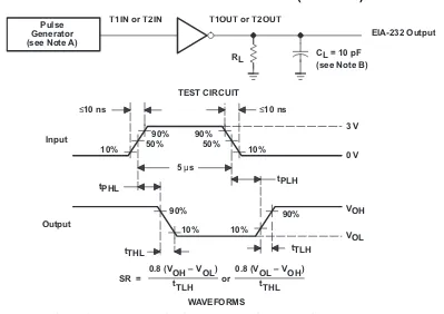
≤10 ns
VCC
R1IN or R2IN
R1OUT or R2OUT
RL = 1.3 kΩ
See Note C
CL = 50 pF (see Note B)
TEST CIRCUIT
≤10 ns
Input
Output
tPHL tPLH
1.5 V
VOL VOH 0 V 3 V
10%
90% 50%
500 ns
WAVEFORMS 1.5 V 90%
50% 10% Pulse
Generator (see Note A)
MAX232, MAX232I
www.ti.com SLLS047M – FEBRUARY 1989 – REVISED NOVEMBER 2014
8 Parameter Measurement Information
A. The pulse generator has the following characteristics: ZO= 50Ω, duty cycle≤50%. B. CLincludes probe and jig capacitance.
C. All diodes are 1N3064 or equivalent.
EIA-232 Output T1IN or T2IN T1OUT or T2OUT
CL = 10 pF
SLLS047M – FEBRUARY 1989 – REVISED NOVEMBER 2014 www.ti.com
Parameter Measurement Information (continued)
A. The pulse generator has the following characteristics: ZO= 50Ω, duty cycle≤50%. B. CLincludes probe and jig capacitance.
5V
www.ti.com SLLS047M – FEBRUARY 1989 – REVISED NOVEMBER 2014
9 Detailed Description
9.1 Overview
The MAX232 device is a dual driver/receiver that includes a capacitive voltage generator using four capacitors to
supply TIA/EIA-232-F voltage levels from a single V supply. Each receiver converts TIA/EIA-232-F inputs to
5-V TTL/CMOS levels. These receivers have a typical threshold of 1.3 5-V, a typical hysteresis of 0.5 5-V, and can
accept ±30-V inputs. Each driver converts TTL/CMOS input levels into TIA/EIA-232-F levels. The driver, receiver,
and voltage-generator functions are available as cells in the Texas Instruments LinASIC™ library. Outputs are
protected against shorts to ground.
9.2 Functional Block Diagram
9.3 Feature Description
9.3.1 Power
The power block increases and inverts the 5V supply for the RS232 driver using a charge pump that requires
four 1-µF external capacitors.
9.3.2 RS232 Driver
Two drivers interface standard logic level to RS232 levels. Internal pull up resistors on TIN inputs ensures a high
input when the line is high impedance.
9.3.3 RS232 Receiver
Two receivers interface RS232 levels to standard logic levels. An open input will result in a high output on ROUT.
9.4 Device Functional Modes
9.4.1 V
CCpowered by 5V
The device will be in normal operation.
9.4.2 V
CCunpowered
When MAX232 is unpowered, it can be safely connected to an active remote RS232 device.
Table 1. Function Table Each Driver
(1)INPUT OUTPUT
TIN TOUT
L H
H L
1µF NOTES: A. Resistor values shown are nominal.
B. Nonpolarized ceramic capacitors are acceptable. If polarized tantalum or electrolytic capacitors are used, they should be connected as shown. In addition to the 1-µF capacitors shown, the MAX202 can operate with 0.1-µF capacitors.
+ +
− = 1 µF
MAX232, MAX232I
SLLS047M – FEBRUARY 1989 – REVISED NOVEMBER 2014 www.ti.com
Table 2. Function Table Each Receiver
(1)INPUTS OUTPUT Open = disconnected input or connected driver off
10 Application and Implementation
NOTE
Information in the following applications sections is not part of the TI component
specification, and TI does not warrant its accuracy or completeness. TI’s customers are
responsible for determining suitability of components for their purposes. Customers should
validate and test their design implementation to confirm system functionality.
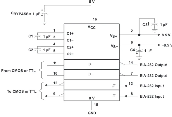
10.1 Application Information
For proper operation add capacitors as shown in
Figure 6
. Pins 9 through 12 connect to UART or general
purpose logic lines. EIA-232 lines will connect to a connector or cable.
10.2 Typical Application
Figure 6. Typical Operating Circuit
VCC
Load resistance (k )
VOL
www.ti.com SLLS047M – FEBRUARY 1989 – REVISED NOVEMBER 2014
Typical Application (continued)
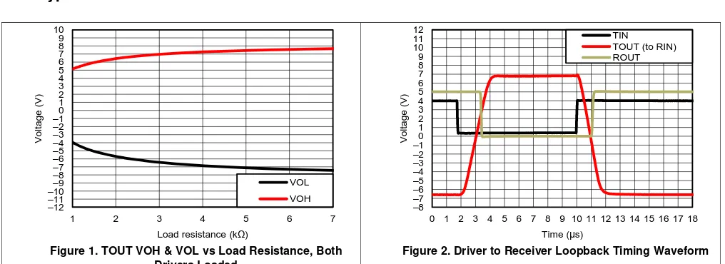
10.2.3 Application Curves
Figure 7. TOUT VOH & VOL vs Load Resistance, Both Figure 8. Driver to Receiver Loopback Timing Waveform Drivers Loaded
11 Power Supply Recommendations
The V
CCvoltage should be connected to the same power source used for logic device connected to TIN pins.
V
CCshould be between 4.5V and 5.5V.
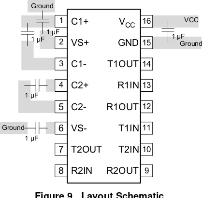
12 Layout
12.1 Layout Guidelines
Keep the external capacitor traces short. This is more important on C1 and C2 nodes that have the fastest rise
and fall times.
12.2 Layout Example
MAX232, MAX232I
SLLS047M – FEBRUARY 1989 – REVISED NOVEMBER 2014 www.ti.com
13 Device and Documentation Support
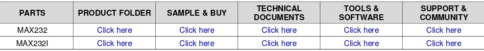
13.1 Related Links
The table below lists quick access links. Categories include technical documents, support and community
resources, tools and software, and quick access to sample or buy.
Table 3. Related Links
TECHNICAL TOOLS & SUPPORT & PARTS PRODUCT FOLDER SAMPLE & BUY
DOCUMENTS SOFTWARE COMMUNITY
MAX232 Click here Click here Click here Click here Click here
MAX232I Click here Click here Click here Click here Click here
13.2 Trademarks
All trademarks are the property of their respective owners.
13.3 Electrostatic Discharge Caution
These devices have limited built-in ESD protection. The leads should be shorted together or the device placed in conductive foam during storage or handling to prevent electrostatic damage to the MOS gates.
13.4 Glossary
SLYZ022
—
TI Glossary.
This glossary lists and explains terms, acronyms and definitions.
14 Mechanical, Packaging, and Orderable Information
PACKAGE OPTION ADDENDUM
Op Temp (°C) Device Marking
(4/5)
Samples
MAX232D ACTIVE SOIC D 16 40 Green (RoHS
& no Sb/Br)
CU NIPDAU Level-1-260C-UNLIM 0 to 70 MAX232
MAX232DE4 ACTIVE SOIC D 16 40 Green (RoHS
& no Sb/Br)
CU NIPDAU Level-1-260C-UNLIM 0 to 70 MAX232
MAX232DG4 ACTIVE SOIC D 16 40 Green (RoHS
& no Sb/Br)
CU NIPDAU Level-1-260C-UNLIM 0 to 70 MAX232
MAX232DR ACTIVE SOIC D 16 2500 Green (RoHS
& no Sb/Br)
CU NIPDAU | CU SN Level-1-260C-UNLIM 0 to 70 MAX232
MAX232DRE4 ACTIVE SOIC D 16 2500 Green (RoHS
& no Sb/Br)
CU NIPDAU Level-1-260C-UNLIM 0 to 70 MAX232
MAX232DRG4 ACTIVE SOIC D 16 2500 Green (RoHS
& no Sb/Br)
CU NIPDAU Level-1-260C-UNLIM 0 to 70 MAX232
MAX232DW ACTIVE SOIC DW 16 40 Green (RoHS
& no Sb/Br)
CU NIPDAU Level-1-260C-UNLIM 0 to 70 MAX232
MAX232DWE4 ACTIVE SOIC DW 16 40 Green (RoHS
& no Sb/Br)
CU NIPDAU Level-1-260C-UNLIM 0 to 70 MAX232
MAX232DWG4 ACTIVE SOIC DW 16 40 Green (RoHS
& no Sb/Br)
CU NIPDAU Level-1-260C-UNLIM 0 to 70 MAX232
MAX232DWR ACTIVE SOIC DW 16 2000 Green (RoHS
& no Sb/Br)
CU NIPDAU Level-1-260C-UNLIM 0 to 70 MAX232
MAX232DWRE4 ACTIVE SOIC DW 16 2000 Green (RoHS
& no Sb/Br)
CU NIPDAU Level-1-260C-UNLIM 0 to 70 MAX232
MAX232DWRG4 ACTIVE SOIC DW 16 2000 Green (RoHS
& no Sb/Br)
CU NIPDAU Level-1-260C-UNLIM 0 to 70 MAX232
MAX232ID ACTIVE SOIC D 16 40 Green (RoHS
& no Sb/Br)
CU NIPDAU Level-1-260C-UNLIM -40 to 85 MAX232I
MAX232IDE4 ACTIVE SOIC D 16 40 Green (RoHS
& no Sb/Br)
CU NIPDAU Level-1-260C-UNLIM -40 to 85 MAX232I
MAX232IDG4 ACTIVE SOIC D 16 40 Green (RoHS
& no Sb/Br)
CU NIPDAU Level-1-260C-UNLIM -40 to 85 MAX232I
PACKAGE OPTION ADDENDUM
Op Temp (°C) Device Marking
(4/5)
Samples
MAX232IDW ACTIVE SOIC DW 16 40 Green (RoHS
& no Sb/Br)
CU NIPDAU Level-1-260C-UNLIM -40 to 85 MAX232I
MAX232IDWG4 ACTIVE SOIC DW 16 40 Green (RoHS
& no Sb/Br)
CU NIPDAU Level-1-260C-UNLIM -40 to 85 MAX232I
MAX232IDWR ACTIVE SOIC DW 16 2000 Green (RoHS
& no Sb/Br)
CU NIPDAU Level-1-260C-UNLIM -40 to 85 MAX232I
MAX232IDWRE4 ACTIVE SOIC DW 16 2000 Green (RoHS
& no Sb/Br)
CU NIPDAU Level-1-260C-UNLIM -40 to 85 MAX232I
MAX232IDWRG4 ACTIVE SOIC DW 16 2000 Green (RoHS
& no Sb/Br)
CU NIPDAU Level-1-260C-UNLIM -40 to 85 MAX232I
MAX232IN ACTIVE PDIP N 16 25 Pb-Free
(RoHS)
CU NIPDAU N / A for Pkg Type -40 to 85 MAX232IN
MAX232INE4 ACTIVE PDIP N 16 25 Pb-Free
(RoHS)
CU NIPDAU N / A for Pkg Type -40 to 85 MAX232IN
MAX232N ACTIVE PDIP N 16 25 Pb-Free
(RoHS)
CU NIPDAU N / A for Pkg Type 0 to 70 MAX232N
MAX232NE4 ACTIVE PDIP N 16 25 Pb-Free
(RoHS)
CU NIPDAU N / A for Pkg Type 0 to 70 MAX232N
MAX232NSR ACTIVE SO NS 16 2000 Green (RoHS
& no Sb/Br)
CU NIPDAU Level-1-260C-UNLIM 0 to 70 MAX232
(1) The marketing status values are defined as follows: ACTIVE: Product device recommended for new designs.
LIFEBUY: TI has announced that the device will be discontinued, and a lifetime-buy period is in effect.
NRND: Not recommended for new designs. Device is in production to support existing customers, but TI does not recommend using this part in a new design.
PREVIEW: Device has been announced but is not in production. Samples may or may not be available.
OBSOLETE: TI has discontinued the production of the device.
PACKAGE OPTION ADDENDUM
www.ti.com 30-Apr-2016
(3) MSL, Peak Temp. - The Moisture Sensitivity Level rating according to the JEDEC industry standard classifications, and peak solder temperature.
(4) There may be additional marking, which relates to the logo, the lot trace code information, or the environmental category on the device.
(5) Multiple Device Markings will be inside parentheses. Only one Device Marking contained in parentheses and separated by a "~" will appear on a device. If a line is indented then it is a continuation
of the previous line and the two combined represent the entire Device Marking for that device.
(6) Lead/Ball Finish - Orderable Devices may have multiple material finish options. Finish options are separated by a vertical ruled line. Lead/Ball Finish values may wrap to two lines if the finish
value exceeds the maximum column width.
Important Information and Disclaimer:The information provided on this page represents TI's knowledge and belief as of the date that it is provided. TI bases its knowledge and belief on information provided by third parties, and makes no representation or warranty as to the accuracy of such information. Efforts are underway to better integrate information from third parties. TI has taken and continues to take reasonable steps to provide representative and accurate information but may not have conducted destructive testing or chemical analysis on incoming materials and chemicals. TI and TI suppliers consider certain information to be proprietary, and thus CAS numbers and other limited information may not be available for release.
TAPE AND REEL INFORMATION
*All dimensions are nominal
Device Package Type
Package Drawing
Pins SPQ Reel Diameter
(mm)
Reel Width W1 (mm)
A0 (mm)
B0 (mm)
K0 (mm)
P1 (mm)
W (mm)
Pin1 Quadrant
MAX232DR SOIC D 16 2500 330.0 16.4 6.5 10.3 2.1 8.0 16.0 Q1
MAX232DR SOIC D 16 2500 330.0 16.4 6.5 10.3 2.1 8.0 16.0 Q1
MAX232DRG4 SOIC D 16 2500 330.0 16.4 6.5 10.3 2.1 8.0 16.0 Q1
MAX232DRG4 SOIC D 16 2500 330.0 16.4 6.5 10.3 2.1 8.0 16.0 Q1
MAX232DWR SOIC DW 16 2000 330.0 16.4 10.75 10.7 2.7 12.0 16.0 Q1
MAX232DWRG4 SOIC DW 16 2000 330.0 16.4 10.75 10.7 2.7 12.0 16.0 Q1
MAX232IDR SOIC D 16 2500 330.0 16.4 6.5 10.3 2.1 8.0 16.0 Q1
MAX232IDWR SOIC DW 16 2000 330.0 16.4 10.75 10.7 2.7 12.0 16.0 Q1
MAX232IDWRG4 SOIC DW 16 2000 330.0 16.4 10.75 10.7 2.7 12.0 16.0 Q1
PACKAGE MATERIALS INFORMATION
*All dimensions are nominal
Device Package Type Package Drawing Pins SPQ Length (mm) Width (mm) Height (mm)
MAX232DR SOIC D 16 2500 333.2 345.9 28.6
MAX232DR SOIC D 16 2500 367.0 367.0 38.0
MAX232DRG4 SOIC D 16 2500 333.2 345.9 28.6
MAX232DRG4 SOIC D 16 2500 367.0 367.0 38.0
MAX232DWR SOIC DW 16 2000 367.0 367.0 38.0
MAX232DWRG4 SOIC DW 16 2000 367.0 367.0 38.0
MAX232IDR SOIC D 16 2500 333.2 345.9 28.6
MAX232IDWR SOIC DW 16 2000 367.0 367.0 38.0
MAX232IDWRG4 SOIC DW 16 2000 367.0 367.0 38.0
PACKAGE MATERIALS INFORMATION
IMPORTANT NOTICE
Texas Instruments Incorporated and its subsidiaries (TI) reserve the right to make corrections, enhancements, improvements and other changes to its semiconductor products and services per JESD46, latest issue, and to discontinue any product or service per JESD48, latest issue. Buyers should obtain the latest relevant information before placing orders and should verify that such information is current and complete. All semiconductor products (also referred to herein as “components”) are sold subject to TI’s terms and conditions of sale supplied at the time of order acknowledgment.
TI warrants performance of its components to the specifications applicable at the time of sale, in accordance with the warranty in TI’s terms and conditions of sale of semiconductor products. Testing and other quality control techniques are used to the extent TI deems necessary to support this warranty. Except where mandated by applicable law, testing of all parameters of each component is not necessarily performed.
TI assumes no liability for applications assistance or the design of Buyers’ products. Buyers are responsible for their products and applications using TI components. To minimize the risks associated with Buyers’ products and applications, Buyers should provide adequate design and operating safeguards.
TI does not warrant or represent that any license, either express or implied, is granted under any patent right, copyright, mask work right, or other intellectual property right relating to any combination, machine, or process in which TI components or services are used. Information published by TI regarding third-party products or services does not constitute a license to use such products or services or a warranty or endorsement thereof. Use of such information may require a license from a third party under the patents or other intellectual property of the third party, or a license from TI under the patents or other intellectual property of TI.
Reproduction of significant portions of TI information in TI data books or data sheets is permissible only if reproduction is without alteration and is accompanied by all associated warranties, conditions, limitations, and notices. TI is not responsible or liable for such altered documentation. Information of third parties may be subject to additional restrictions.
Resale of TI components or services with statements different from or beyond the parameters stated by TI for that component or service voids all express and any implied warranties for the associated TI component or service and is an unfair and deceptive business practice. TI is not responsible or liable for any such statements.
Buyer acknowledges and agrees that it is solely responsible for compliance with all legal, regulatory and safety-related requirements concerning its products, and any use of TI components in its applications, notwithstanding any applications-related information or support that may be provided by TI. Buyer represents and agrees that it has all the necessary expertise to create and implement safeguards which anticipate dangerous consequences of failures, monitor failures and their consequences, lessen the likelihood of failures that might cause harm and take appropriate remedial actions. Buyer will fully indemnify TI and its representatives against any damages arising out of the use of any TI components in safety-critical applications.
In some cases, TI components may be promoted specifically to facilitate safety-related applications. With such components, TI’s goal is to help enable customers to design and create their own end-product solutions that meet applicable functional safety standards and requirements. Nonetheless, such components are subject to these terms.
No TI components are authorized for use in FDA Class III (or similar life-critical medical equipment) unless authorized officers of the parties have executed a special agreement specifically governing such use.
Only those TI components which TI has specifically designated as military grade or “enhanced plastic” are designed and intended for use in military/aerospace applications or environments. Buyer acknowledges and agrees that any military or aerospace use of TI components which havenotbeen so designated is solely at the Buyer's risk, and that Buyer is solely responsible for compliance with all legal and
regulatory requirements in connection with such use.
TI has specifically designated certain components as meeting ISO/TS16949 requirements, mainly for automotive use. In any case of use of non-designated products, TI will not be responsible for any failure to meet ISO/TS16949.
Products Applications
Audio www.ti.com/audio Automotive and Transportation www.ti.com/automotive
Amplifiers amplifier.ti.com Communications and Telecom www.ti.com/communications
Data Converters dataconverter.ti.com Computers and Peripherals www.ti.com/computers
DLP® Products www.dlp.com Consumer Electronics www.ti.com/consumer-apps
DSP dsp.ti.com Energy and Lighting www.ti.com/energy
Clocks and Timers www.ti.com/clocks Industrial www.ti.com/industrial
Interface interface.ti.com Medical www.ti.com/medical
Logic logic.ti.com Security www.ti.com/security
Power Mgmt power.ti.com Space, Avionics and Defense www.ti.com/space-avionics-defense
Microcontrollers microcontroller.ti.com Video and Imaging www.ti.com/video
RFID www.ti-rfid.com
OMAP Applications Processors www.ti.com/omap TI E2E Community e2e.ti.com
Wireless Connectivity www.ti.com/wirelessconnectivity
HANWEI ELETRONICS CO.,LTD MQ-2 http://www.hwsensor.com
They are used in gas leakage detecting equipments in family and industry, are suitable for detecting
of LPG, i-butane, propane, methane ,alcohol, Hydrogen, smoke.
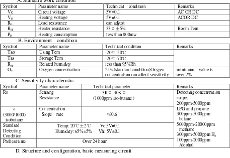
SPECI FI CAT ION S
A. Standard work condition
Symbol Parameter name Technical condition Remarks
Vc Circuit voltage 5V±0.1 AC OR DC
Symbol Parameter name Technical condition Remarks
Tao Using Tem -20℃-50℃
Tas Storage Tem -20℃-70℃
RH Related humidity less than 95%Rh
O2 Oxygen concentration 21%(standard condition)Oxygen
concentration can affect sensitivity
minimum value is
Configuration A Configuration B
HANWEI ELETRONICS CO.,LTD MQ-2 http://www.hwsensor.com
crust made by plastic and stainless steel net. The heater provides necessary work conditions for work of
sensitive components. The enveloped MQ-2 have 6 pin ,4 of them are used to fetch signals, and other 2 are used
for providing heating current.
Electric parameter measurement circuit is shown as Fig.2
Resistance value of MQ-2 is difference to various kinds and various concentration gases. So,When using
this components, sensitivity adjustment is very necessary. we recommend that you calibrate the detector for
1000ppm liquified petroleum gas<LPG>,or 1000ppm iso-butane<i-C4H10>concentration in air and use value
ofLoad resistance that( R
L) about 20 K
Ω
(5K
Ω
to 47 K
Ω
).
When accurately measuring, the proper alarm point for the gas detector should be determined after
considering the temperature and humidity influence.
Fig.3 is shows the typical
sensitivity characteristics of
the MQ-2 for several gases.
in their: Temp: 20℃、
Humidity: 65%、
O2 concentration 21%
RL=5kΩ
Ro: sensor resistance at 1000ppm of
H2 in the clean air.
Rs:sensor resistance at various concentrations of gases.
Fig.4 is shows the typical dependence of
the MQ-2 on temperature and humidity.
Ro: sensor resistance at 1000ppm of H2 in air
at 33%RH and 20 degree.
Rs: sensor resistance at 1000ppm of H2
at different temperatures and humidities.