Other uses, including reproduction and distribution, or selling or
licensing copies, or posting to personal, institutional or third party
websites are prohibited.
In most cases authors are permitted to post their version of the
article (e.g. in Word or Tex form) to their personal website or
institutional repository. Authors requiring further information
regarding Elsevier’s archiving and manuscript policies are
encouraged to visit:
Fabrication of high-performance
fl
uorine doped
–
tin oxide
fi
lm using
fl
ame-assisted
spray deposition
Agus Purwanto
a,⁎
, Hendri Widiyandari
b, Arif Jumari
aaDepartment of Chemical Engineering, Faculty of Engineering, Sebelas Maret University, Jl. Ir. Sutami 36 A, Surakarta, Central Java 57126, Indonesia b
Department of Physics, Faculty of Mathematics and Natural Sciences, Diponegoro University, Jl. Prof. Dr. Soedarto, Tembalang, Semarang 50275, Indonesia
a b s t r a c t
a r t i c l e
i n f o
Article history:
Received 5 September 2010
Received in revised form 6 August 2011 Accepted 9 August 2011
A high-performancefluorine–doped tin oxide (FTO)film was fabricated byflame-assisted spray deposition method. By varying the NH4F doping concentration, the optimal concentration was established as 8 at.%. X-ray
diffractograms confirmed that the as-grown FTOfilm was tetragonal SnO2. In addition, the FTOfilm was
comprised of nano-sized grains ranging from 40 to 50 nm. The heat-treated FTOfilm exhibited a sheet resistance of 21.8Ω/ with an average transmittance of 81.9% in the visible region (λ= 400–800 nm). The
figures of merit shows that the prepared FTOfilm can be used for highly efficient dye-sensitized solar cells electrodes.
© 2011 Elsevier B.V. All rights reserved.
1. Introduction
Fluorine–doped tin oxide (FTO)film is widely used for optoelec-tronic applications such as displays, solar cells, light emitting diodes, smart windows, etc.[1]. Compared to indium–doped tin oxide (ITO), FTO has many advantages such as low cost, chemical resistance, and high availability of precursor sources[1,2]. In addition, ITO suffered from low electrical conductivity after annealing treatment in an oxygen atmosphere during fabrication of dye-sensitized solar cells (DSSCs)[3,4]. This case was not found in the application of FTO as electrodes for DSSCs. Therefore, FTO would be an economically viable and a best candidate for DSSCs electrodes.
The fabrication of FTO thin films has been reported by various methods, which includes spray pyrolysis deposition (SPD) [2,5,6], sputtering[7], and chemical vapor deposition[8]. The SPD method is the most popular due to its simplicity, low cost, and scale-up ease
[2,5,9,10]. Several modifications of the SPD method have been
reported, such as the application of lamp radiation for a substrate heater[11], electricfield induction[10], and the use of an ultrasonic nebulizer as a droplet generator[12,13]. Recently, a class of deposition technique of flame-assisted spray deposition (FASD) has been introduced as an alternative low-cost method for film deposition
[4,14–18]. Several materials have been fabricated using this method,
such as ITO[4], Pt–ZnO[18], TiO2[17], and yttria–stabilized zirconia
[16]. However, the preparation FTOfilm using FASD method was not
found in the literatures.
In this paper, we report the fabrication of FTOfilm using the FASD route. The effect of flow configuration, doping concentration, substrate temperature, and heat-treatment were investigated sys-tematically. An ultrasonic nebulizer was used to atomize an aqueous precursor with a controllable droplet speed (size of 5μm)[19]. The configuration of precursor dropletflow controlled the characteristic of the prepared FTOfilm. In addition, substrate temperature and heat treatment were highly affected on the electrical conductivity of as-prepared FTOfilm. In this investigation, the high performance FTO films that showed good electrical conductivity, transparency, andfilm adhesion could be produced by FASD method.
2. Experimental details
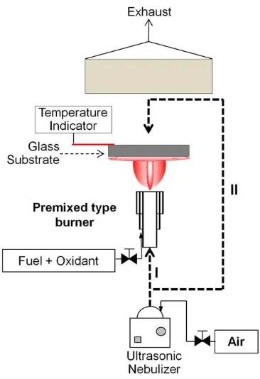
The schematic diagram of the FASD system is shown inFig. 1. In accordance with the FASD technique, the substrate (soda lime glass) was located above a burner. The temperature of the substrate was monitored using a thermometer (K-type thermocouple, Fluke 51, Fluke Corporation, Washington, United States). The substrate tem-perature was controlled from 300 to 420 °C. This temtem-perature range is the operation temperatures of the experimental devices. The droplet was transported through the center of the burner and deposited on the bottom-side of glass substrate (Fig. 1, configuration I). In configuration II, droplets were transported to the upper-side of glass
⁎Corresponding author. Tel./fax: +62 271 632112.
E-mail address:[email protected](A. Purwanto).
0040-6090/$–see front matter © 2011 Elsevier B.V. All rights reserved. doi:10.1016/j.tsf.2011.08.041
Contents lists available atSciVerse ScienceDirect
Thin Solid Films
substrate. The heating of substrate was conducted from the below-side of substrate. Prior flowing of droplets to the substrate, the substrate was heated to the designated temperature. When the desired temperature achieved, the droplets were then transported to the upper side of the glass substrate. For all experiments, an ultrasonic nebulizer was used to generate droplets of the precursor at a frequency of 1.7 MHz (Omron NE-U22V, Tokyo, Japan). The precursor was an aqueous solution of SnCl2. 2H2O (98%, Merck Ltd., Germany) and NH4F (98%, Merck Ltd., Germany) in 0.5 N HCl. The FTOfilms were prepared at various NH4F concentrations (6 at.%–14 at.%). To improve the conductivity of thefilms, annealing was conducted at elevated temperatures (450–550 °C).
The sheet resistance (Rs) of the FTOfilms was evaluated using four-probe measurements (Jandel Engineering, Bedfordshire, UK). The optical properties of the FTOfilms were evaluated using a UV–Vis spectrophotometer (UV 2450, Shimadzu, Kyoto, Japan). Thefigure of merit was calculated using a Haacke equation (ΦTC=T10/Rs)[20]and MTC for application in dye sensitized solar cells (DSSCs)[13]. This figure of merit was calculated using equation:
MTC= 0ð :769−0:0868T−0:000287Rs−0:00207T:RsÞð1:23 + 18:99TÞ
whereTis transmittance. To evaluate the crystal structure, thefilms were characterized using an X-ray diffractometer (XRD, RINT 2200V, Rigaku-Denki Corp., Tokyo, Japan). The XRD measurements were carried out using nickel-filtered CuKα radiation (λ= 0.154 nm) at 40 kV and 30 mA. The XRD measurements were carried out using nickel-filtered Cu Kα(λ= 0.154 nm) at 40 kV and 30 mA with a scan step of 0.02° and a scan speed of 4°/min. The morphology of the FTO film was evaluated usingfield emission-scanning electron microscopy (FE-SEM) observations with an S-5000 at 20 kV (Hitachi Ltd., Tokyo, Japan). Prior to FE-SEM characterization, the sputtering treatment was not conducted because the FTOfilm is conductive.
3. Results and discussion
The investigation of FTO fabrication using FASD method was started by the evaluation of dropletsflow configurations as indicated
inFig. 1. In configuration I, droplets were suplied to the bottom side of
the glass substrate. The substrate was positioned at 10 cm above the burner with the deposition temperature at 420 °C for 25 min. The resistivity of the as-prepared FTOfilm can be found inTable 1. All samples had resistivity in the MΩ order and the film was heterogeneous in surface. In addition, the X-ray characterization indicated that the FTOfilm was amorphous (Fig. 2). Annealing at 550 °C for 1 h did not improve the crystallinity significantly. The unexpected characteristics of FTOfilm prepared by FASP-confi gura-tion I can be concluded from imperfect crystalizagura-tion FTOfilm.
Since FASD-configuration I did not produce FTO film with the expected characteristics, FASD-Configuration II was then examined. Using this configuration, good characteristics of FTO film can be fabricated. The dependency of sheet resistance (Rs) as a function of doping concentration is shown in Fig. 3. The present study was conducted using a precursor concentration of 0.5 M. The deposition process was conducted for 10 min. To evaluate the effect of doping concentrations (6–14 at.%), the substrate temperature was main-tained at 420 °C. AsFig. 3shows, the optimal doping concentration was 8 at.%. The conductivity of the FTO film originated from the substitution offluorine atoms in the SnO2lattice. The substitution of oxygen ions withfluorine ions leaving an oxygen vacancy suggests the conduction of electrons by the SnO2 film [6,11]. When doping concentration is above the optimal level (8 at.%), the Rs increase. The high Rsoriginated from an accumulation offluorine in the grain boundaries[6]. Then, thisfluorine concentration level was used in all experimentation.
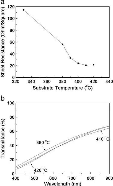
Substrate temperature is an important parameter in controlling FTO film characteristics. Fig. 4 shows the dependency of Rs and transmittance on substrate temperatures.Fig. 4a showed a decrease in Rs when the substrate temperature was elevated. The optimal temperature for FTO film preparation ranged from 410 to 420 °C (Rs= 20.5–21.5Ω/ ). Unfortunately, the light transmittance (T) of the as-prepared FTOfilms deposited for 10 min was low (21.7–25.9%), as
Fig. 1.Schematic diagram of the FASD method.
Table 1
The FTOfilm characteristics prepared by FASD-configuration I route.
Doping level (at.%) Resistivity (MΩ, measured in 1 cm apart)
10 Not conductive
shown inFig. 4b. The increasing deposition temperature improved the crystallinity of FTOfilm. As a result, electron mobility and conductivity are improved due to less grain boundaries[21]. For comparison, the optimal temperature for FTO deposition using SPD method ranges from 400 to 450 °C[13,21].
To increase the light transmittance, the deposition time and precursor concentration were reduced to 5 min and 0.1 M (doping concentration 8 at.%), respectively. Using this strategy, film with a high transmittance (T= 81.9%) was produced, as shown inFig. 5b. However, the Rsof the as-prepared FTOfilm dropped significantly to 254.2Ω/ (Fig. 5a). To improve the electrical conductivity, an annealing treatment under atmospheric conditions was conducted (450–550 °C; 30 min). As expected, the Rsof the FTOfilm was enhanced
to 21.8Ω/ (500 °C,Fig. 5a) with no loss of light transmittance (Fig. 5b (inset: high transmittance of FTOfilm)). Thus, the combination of FASD and annealing treatment could be used to produce high-performance FTOfilm. Thefigure of merit (ΦTC) of the FTOfilm annealed at 500 °C was 1.1 × 10⁻²Ω−1, which is comparable to other methods (in the
order 10−2Ω−1)[6,11,22]. Evaluation usingfigures of merit for a DSSC
application (MTC) showed a value of 11.5. For comparison, theMTCvalue of FTO prepared by spray pyrosol technique can reach approximately 11.2 which can be used to produce DSSC solar cell with the efficiency around 7%[13]. This result indicated that the prepared FASD-FTOfilm was ideal for a high-efficiency DSSC solar cell electrode[13].
Fig. 6 shows an XRD pattern on the films before and after
annealment at 500 °C for 30 min. The crystalline structure of the FTO films was tetragonal SnO2(JCPDS no. 770451, and space group: F42/ mnm(136)). The XRD pattern also confirmed that annealing in elevated temperatures improved the crystallinity of the FTOfilms. The crystallite sizes FTOfilm were 27 nm, and 34 nm for the film without, and after annealing at 500 °C, respectively. This produced better electrical conductivity, as shown in Fig. 5a. From XRD diffractograms, it is also shown that the crystal orientations of the film were same. This suggested that improvement of electrical conductivity only originated from the enhancement of the FTOfilm crystallinity.
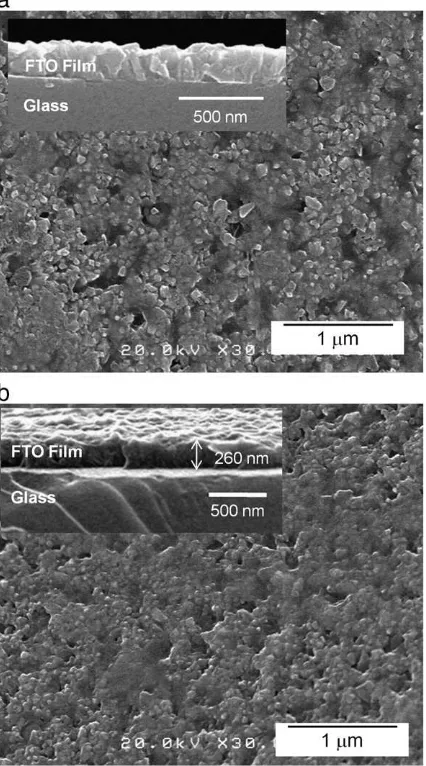
The morphology of the as-prepared FTOfilms was characterized using FE-SEM. Fig. 7a and b shows FE-SEM images of FTO film prepared by FASD before and after annealing, respectively. The FTO film was composed of small grains ranging from 40 to 50 nm. This size was larger compared to the XRD calculation. This discrepancy may originate from the different basis of calculation. Using XRD diffracto-grams, crystal size of FTO was calculated using Scherer's equation. On the other hand, grain size measured from the SEM images predicted the particle size regarding the crystal nature of thefilms. Annealing at 500 °C for 30 min did not alter the grain size much as indicated in
Fig. 3.Sheet resistance of FTOfilm prepared using FASD-configuration II as a function of doping concentration.
Fig. 4.Sheet resistance (a) and light transmittance (b) of FTOfilm as a function of substrate temperature.
Fig. 7b. The cross-sectional images showed that the thickness of the FTOfilm was approximately 260 nm. The calculated specific resistivity of the heat treated-FTOfilm was 5.67 × 10⁻⁵Ωcm. For comparison,
the specific resistivity of FTOfilm prepared by pyrosol method was averagely 5 × 10⁻⁴Ωcm[12]. Thus, the specific resistivity of
FASD-prepared FTOfilm is in comparable with the other method.
4. Conclusion
A high performance of FTO film was fabricated using a FASD technique. The droplet supplied technique controlled the perfor-mance of the as-prepared FTOfilm. Droplet supplying to the top-side of substrate produced FTOfilm with good characteristics. With this method, the optimal doping concentration offluorine was 8 at.%. The FASD method combined with post-treatment (500 °C for 30 min) produced a highly conductive FTO film (sheet resistance 21.8Ω/ ) with high light transmittance (81.9%). Afigure of merit calculation showed a value that is incomparable with other methods. We showed that the FASD method is a method that can be applied in the production of relatively large-area, high-performance FTOfilms.
Acknowledgment
The authors wish to thank the DGHE-Ministry of National Education of Indonesia for providing the research funding through the Hibah Kompetitif Penelitian Sesuai Prioritas Nasional Batch II, 2009–2010 with contract number 22/SP2H/PP/DP2M/VI/2009–2010.
References
[1] R. Kumar, C. Zhou, ACS Nano 4 (2010) 11.
[2] M. Adnane, H. Cachet, G. Folcher, S. Hamzaoui, Thin Solid Films 492 (2005) 240. [3] C. Sima, C. Grigoriu, S. Antohe, Thin Solid Films 519 (2010) 595.
[4] A. Purwanto, H. Widiyandari, D. Hidayat, F. Iskandar, K. Okuyama, Chem. Mater. 21 (2009) 4087.
[5] E. Elangovan, M.P. Singh, M.S. Dharmaprakash, K. Ramamurthi, J. Optoelectron. Adv. Mater. 6 (2004) 197.
[6] A.V. Moholkar, S.M. Pawar, K.Y. Rajpure, C.H. Bhosale, J.H. Kim, Appl. Surf. Sci. 255 (2009) 9358.
[7] B. Stjerna, E. Olsson, C.G. Granqvist, J. Appl. Phys. 76 (1994) 3797. [8] J.H. Park, D.J. Byun, J.K. Lee, J. Electroceram. 23 (2009) 506.
[9] M.A. Aouaj, R. Diaz, A. Belayachi, F. Rueda, M. Abd-Lefdil, Mater. Res. Bull. 44 (2009) 1458.
[10] A. Gupta, D.K. Pandya, S.C. Kashyap, Jpn. J. Appl. Phys., Part 2 43 (2004) L1592. [11] M. Soliman, M.M. Hussein, S. El-Atawy, M. El-Gamal, Renewable Energy 23 (2001)
463.
[12] B. Gottlieb, R. Koropecki, R. Arce, R. Crisalle, J. Ferro, Thin Solid Films 199 (1991) 13.
[13] X. Huang, Y. Zhang, H. Sun, D. Li, Y. Luo, Q. Meng, J. Renewable Sustainable Energy 1 (2009) 063107.
[14] G.T. Lim, H.G. Jeong, I.S. Hwang, B.H. Kim, K.H. Kim, J. Park, D.L. Cho, Surf. Coat. Technol. 204 (2010) 3393.
[15] K. Sahner, H.L. Tuller, J. Electroceram. 24 (2010) 177.
[16] H. You, K. Cho, Y. Yoon, J. Im, D. Shin, J. Anal. Appl. Pyrolysis 81 (2008) 14. [17] E. Thimsen, N. Rastgar, P. Biswas, J. Phys. Chem. C 112 (2008) 4134.
[18] N. Tamaekong, C. Liewhiran, A. Wisitsoraat, S. Phanichphant, Sensors 9 (2009) 6652.
[19] W.N. Wang, A. Purwanto, I.W. Lenggoro, K. Okuyama, H. Chang, H.D. Jang, Ind. Eng. Chem. Res. 47 (2008) 1650.
[20] G. Haacke, J. Appl. Phys. 47 (1976) 4086.
[21] C.C. Lin, M.C. Chiang, Y.W. Chen, Thin Solid Films 518 (2009) 1241. [22] E. Elangovan, K. Ramamurthi, J. Optoelectron. Adv. Mater. 5 (2003) 45.
Fig. 6.XRD pattern of FTOfilms before and after annealed at temperature 500 °C (for 30 min).